

Page 1

INTEGRATED CIRCUITS
DATA SH EET
TDA6101Q
Video output amplifier
Preliminary specification
Supersedes data of November 1991
File under Integrated Circuits, IC02
Philips Semiconductors
1995 Feb 07
Page 2

Philips Semiconductors Preliminary specification
Video output amplifier TDA6101Q
FEATURES
• High bandwidth and high slew rate
• No external heatsink required
• Black-current measurement output for Automatic
Black-current Stabilization (ABS)
GENERAL DESCRIPTION
The TDA6101Q is a video output amplifier with 9 MHz
bandwidth. The device is contained in a single in-line 9-pin
medium power (DBS9MPF) package, using high-voltage
DMOS technology, intended to drive the cathode of a
colour CRT.
• Two cathode outputs; one for DC currents, and one for
transient currents
• A feedback output separated from the cathode outputs
• Internal protection against positive appearing
Cathode-Ray Tube (CRT) flashover discharges
• ESD protection
• Simple application with a variety of colour decoders
• Differential input with a designed maximum common
mode input capacitance of 3 pF, a maximum differential
mode input capacitance of 0.5 pF and a differential input
voltage temperature drift of 20 µV/K
• Defined switch-off behaviour.
QUICK REFERENCE DATA
SYMBOL PARAMETER CONDITIONS MIN. TYP. MAX. UNIT
V
V
I
DDH
I
DDL
V
V
T
T
DDH
DDL
I
oc
stg
amb
, V
fb
high level supply voltage 0 − 250 V
low level supply voltage 0 − 14 V
quiescent high voltage supply current Voc= 0.5V
quiescent low voltage supply current Voc= 0.5V
DDH
DDH
input voltage 0 − V
output voltage V
3.5 4.4 5.5 mA
2.2 2.8 3.5 mA
DDL
DDL
− V
DDH
storage temperature −55 − +150 °C
operating ambient temperature −20 − +65 °C
V
V
ORDERING INFORMATION
TYPE NUMBER
TDA6101Q DBS9MPF plastic DIL-bent-SIL medium power package with fin; 9 leads SOT111-1
1995 Feb 07 2
PACKAGE
NAME DESCRIPTION VERSION
Page 3
Philips Semiconductors Preliminary specification
Video output amplifier TDA6101Q
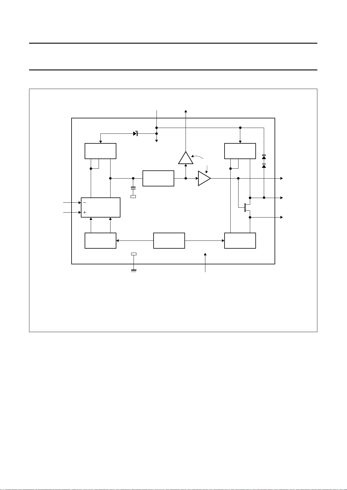
BLOCK DIAGRAM
handbook, full pagewidth
inverting
input
non-inverting
input
3
1
MIRROR
DIFFERENTIAL
STAGE
MIRROR
supply voltage
input HIGH
6
7 V
V
bias
C
par
feedback
output
9
MIRROR
FOLLOWERS
TDA6101Q
CURRENT
SOURCE
42
ground
(substrate)
supply voltage
input LOW
MIRROR
MCD356
7
8
5
cathode
transient
output
cathode
DC output
black current
measurement
output
1995 Feb 07 3
Fig.1 Block diagram.
Page 4
Philips Semiconductors Preliminary specification
Video output amplifier TDA6101Q
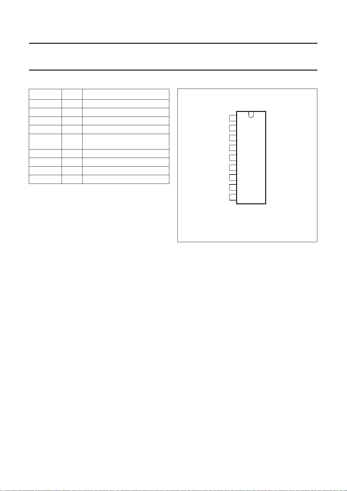
PINNING
SYMBOL PIN DESCRIPTION
V
ip
V
DDL
V
in
GND 4 ground, substrate
I
om
V
DDH
V
cn
V
oc
V
fb
1 non-inverting voltage input
2 supply voltage LOW
3 inverting voltage input
5 black current measurement
output
6 supply voltage HIGH
7 cathode transient voltage output
8 cathode DC voltage output
9 feedback voltage output
handbook, halfpage
V
V
V
DDL
V
GND
I
om
DDH
V
V
V
1
ip
2
3
in
4
TDA6101Q
5
6
7
cn
8
oc
9
fb
MCD355
Fig.2 Pin configuration.
1995 Feb 07 4
Page 5

Philips Semiconductors Preliminary specification
Video output amplifier TDA6101Q
LIMITING VALUES
In accordance with the Absolute Maximum Rating System (IEC 134). Voltages measured with respect to GND (pin 4);
currents as specified in Fig.1; unless otherwise specified.
SYMBOL PARAMETER CONDITIONS MIN. MAX. UNIT
V
DDH
V
DDL
V
I
V
Idm
V
om
V
oc
V
fb
I
in,Iip
I
ocsmL
I
ocsmH
P
tot
T
stg
T
j
V
es
high level supply voltage 0 250 V
low level supply voltage 0 14 V
input voltage 0 V
DDL
V
differential mode input voltage −6+6V
measurement output voltage 0 V
cathode output voltage V
feedback output voltage V
DDL
DDL
V
V
DDL
DDH
DDH
V
V
input current 0 1 mA
low non-repetitive peak cathode
flashover discharge = 100 µC05A
output current
high non-repetitive peak cathode
flashover discharge = 100 nC 0 10 A
output current
total power dissipation 0 1.9 W
storage temperature −55 +150 °C
junction temperature −20 +150 °C
electrostatic handling
human body model (HBM) − > 1500 V
machine model (MM) − > 400 V
HANDLING
Inputs and outputs are protected against electrostatic discharge in normal handling. However, to be totally safe, it is
desirable to take normal precautions appropriate to handling MOS devices (see
“Handling MOS Devices”
).
QUALITY SPECIFICATION
Quality specification
“SNW-FQ-611 part E”
values”, and can be found in the
“Quality reference handbook”
is applicable, except for ESD Human body model see Chapter “Limiting
(ordering number 9398 510 63011).
THERMAL CHARACTERISTICS
SYMBOL PARAMETER
R
R
th j-a
th j-c
thermal resistance from junction to ambient in free air 56 K/W
thermal resistance from junction to case 12 K/W
(1)
VALUE UNIT
Note
1. External heatsink not required.
1995 Feb 07 5
Page 6

Philips Semiconductors Preliminary specification
Video output amplifier TDA6101Q
CHARACTERISTICS
Operating range: T
Vom=1.4VtoV
Test conditions (unless otherwise specified): T
(CL consists of parasitic and cathode capacitance); measured in test circuit Fig.3.
SYMBOL PARAMETER CONDITIONS MIN. TYP. MAX. UNIT
I
DDH
I
DDL
I
bias
I
offset
I
om(offset)
∆I
om
-----------∆I
oc
V
offset
V
oc(min)
V
oc(max)
quiescent HIGH voltage supply current Voc= 0.5V
quiescent LOW voltage supply current Voc= 0.5V
input bias current Voc= 0.5V
input offset current Voc= 0.5V
offset current of measurement output Ioc=0µA;
linearity of current transfer −10 µA<I
input offset voltage Voc= 0.5V
minimum output voltage V
maximum output voltage V
GB gain-bandwidth product of open-loop
gain: V
B
S
B
L
t
pd
small signal bandwidth V
large signal bandwidth V
cathode output propagation delay time
50% input to 50% output
t
r
cathode output rise time 10% output to
90% output
t
f
cathode output fall time 90% output to
10% output
t
s
settling time 50% input to
(99% < output < 101%)
SR slew rate between 50 V to 150 V V
= −20 to 65 °C; V
amb
.
DDL
fb/Vi, dm
= 180 to 210 V; V
DDH
=25°C; V
amb
= 10.8 to 13.2 V; Vip= 2.6 to 5 V;
DDL
DDH
DDH
DDH
DDH
DDH
= 200 V; V
= 12 V; Vip=5V; Vom=6V; CL=10pF
DDL
3.5 4.4 5.5 mA
2.2 2.8 3.5 mA
0 − 20 µA
−3 − +3 µA
−50+5µA
−1.0V<V
1.4 V < Vom<V
−1.0V<V
1.4 V < Vom<V
= −1V −−20 V
1−3
= −1V V
1−3
f = 500 kHz; V
= 60 V (p-p);
ocAC
V
= 100 V
ocDC
= 100 V (p-p);
ocAC
V
= 100 V
ocDC
V
= 100 V (p-p);
ocAC
V
= 100 V square
ocDC
< 1.0 V;
1−3
< 3 mA;
oc
< 1.0 V;
1−3
DDH
DDL
0.9 1.0 1.1
DDL
−50 − +50 mV
− 12 −−V
DDH
= 100 V − 0.8 − GHz
ocDC
79−MHz
5.5 7 − MHz
27 38 49 ns
wave; f < 1 MHz;
tr=tf=40ns;
see Figs 4 and 5
Voc= 50 to 150 V square
43 55 68 ns
wave; f < 1 MHz; tf= 40 ns;
see Fig.4
Voc= 150 to 50 V square
43 55 68 ns
wave; f < 1 MHz; tr= 40 ns;
see Fig.5
V
= 100 V (p-p);
ocAC
V
= 100 V square
ocDC
−−350 ns
wave; f < 1 MHz;
tr=tf=40ns;
see Figs 4 and 5
= 2 V (p-p) square
1−3
− 1700 − V/µs
wave; f < 1 MHz;
tr=tf=40ns
1995 Feb 07 6
Page 7

Philips Semiconductors Preliminary specification
Video output amplifier TDA6101Q
SYMBOL PARAMETER CONDITIONS MIN. TYP. MAX. UNIT
O
v
SVRRH high supply voltage rejection ratio f < 50 kHz; note 2 − 85 − dB
SVRRL low supply voltage rejection ratio f < 50 kHz; note 2 − 70 − dB
Notes
1. If the difference between V
2. SVRR: The ratio of the change in supply voltage to the change in input voltage when there is no change in output
voltage.
Cathode output
The cathode output is protected against peak currents
(caused by positive voltage peaks during high-resistance
flash) of 5 A maximum with a charge content of 100 µC.
The cathode is also protected against peak currents
(caused by positive voltage peaks during low-resistance
flash) of 10 A maximum with a charge content of 100 nC.
Flashover protection
The TDA6101Q incorporates protection diodes against
CRT flashover discharges that clamp the cathode output
pin to the V
has to be within the operating range of 180 to 210 V to
ensure that the Absolute Maximum Rating for V
250 V will not be exceeded during flashover. To limit the
diode current, an external 820 Ω carbon high-voltage
resistor in series with the cathode output and a 2 kV spark
gap are needed (for this resistor-value, the CRT has to be
connected to the main PCB). This addition produces an
increase in the rise and fall times of approximately 5 ns
and a decrease in the overshoot of approximately 3%.
cathode output voltage overshoot V
and Vip is less than 7 V, overshoot cannot be specified.
DDL
pin. The DC supply voltage at the V
DDH
DDH
DDH
= 100 V (p-p);
ocAC
V
= 100 V square
ocDC
wave; f < 1 MHz;
tr=tf=40ns;
see Figs 4 and 5; note 1
V
to GND must be decoupled:
DDH
1. With a capacitor >20 nF with good HF behaviour
(e.g. foil). This capacitance must be placed as close
as possible to pins 6 and 4, but definitely within 5 mm.
2. With a capacitor >10 µF on the picture tube base print
(common for three output stages).
V
to GND must be decoupled:
DDL
1. With a capacitor >20 nF with good HF behaviour
(e.g. ceramic). This capacitance must be placed as
close as possible to pins 2 and 4, but definitely within
10 mm.
pin
Switch-off behaviour
of
The switch-off behaviour of the TDA6101Q is defined:
when the bias current becomes zero, at V
than approximately 5 V, all the output pins
(pins 7, 8 and 9) will be high.
− 9 − %
(pin 2) lower
DDL
1995 Feb 07 7
Page 8
Philips Semiconductors Preliminary specification
Video output amplifier TDA6101Q
handbook, full pagewidth
V
i
R1
50 Ω
C1
22 nF
C2
22 µF
2.7 pF
820 Ω
1.4 mA
C3
R9
12 V 200 V
C
par
C5
22 nF
C4
R10
68.1 kΩ
3926
10 µF
TDA6101Q
1458
A
5 V
C10
100 nF
V
om
6 V
C7
3.2 pF
C6
100 nF
C7 10 µF
7
C8
6.8 pF
C9
136 pF
C
n
560 pF
R3
20 MΩ
R2
1 MΩ
MCD357
probe
C
= 150fF.
par
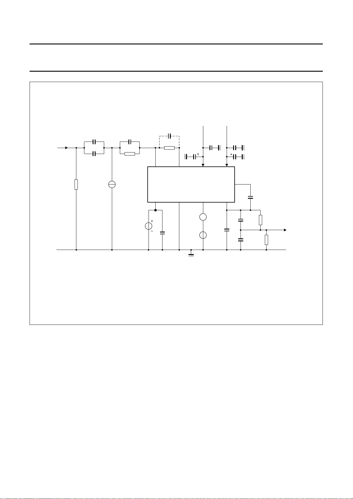
Fig.3 Test circuit with feedback factor1⁄83.
1995 Feb 07 8
Page 9
Philips Semiconductors Preliminary specification
Video output amplifier TDA6101Q
x
V
i
0
x
t
s
overshoot (in %)
150
140
V
oc
100
60
50
t
r
t
pd
t
151
149
t
MGA974
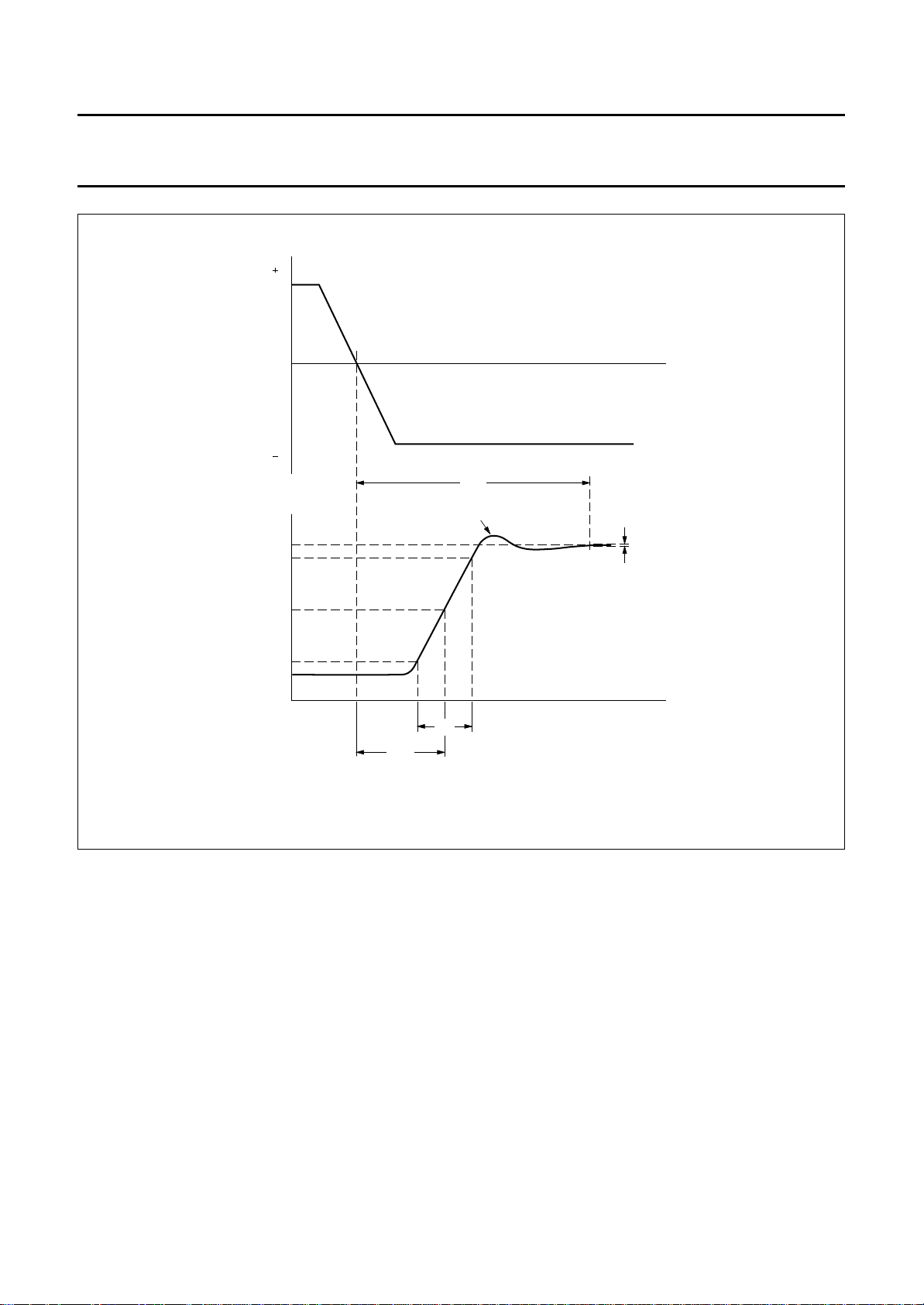
Fig.4 Output voltage (pin 8) rising edge as a function of the AC input signal.
1995 Feb 07 9
Page 10
Philips Semiconductors Preliminary specification
Video output amplifier TDA6101Q
x
V
i
0
x
t
s
150
140
V
oc
100
overshoot (in %)
60
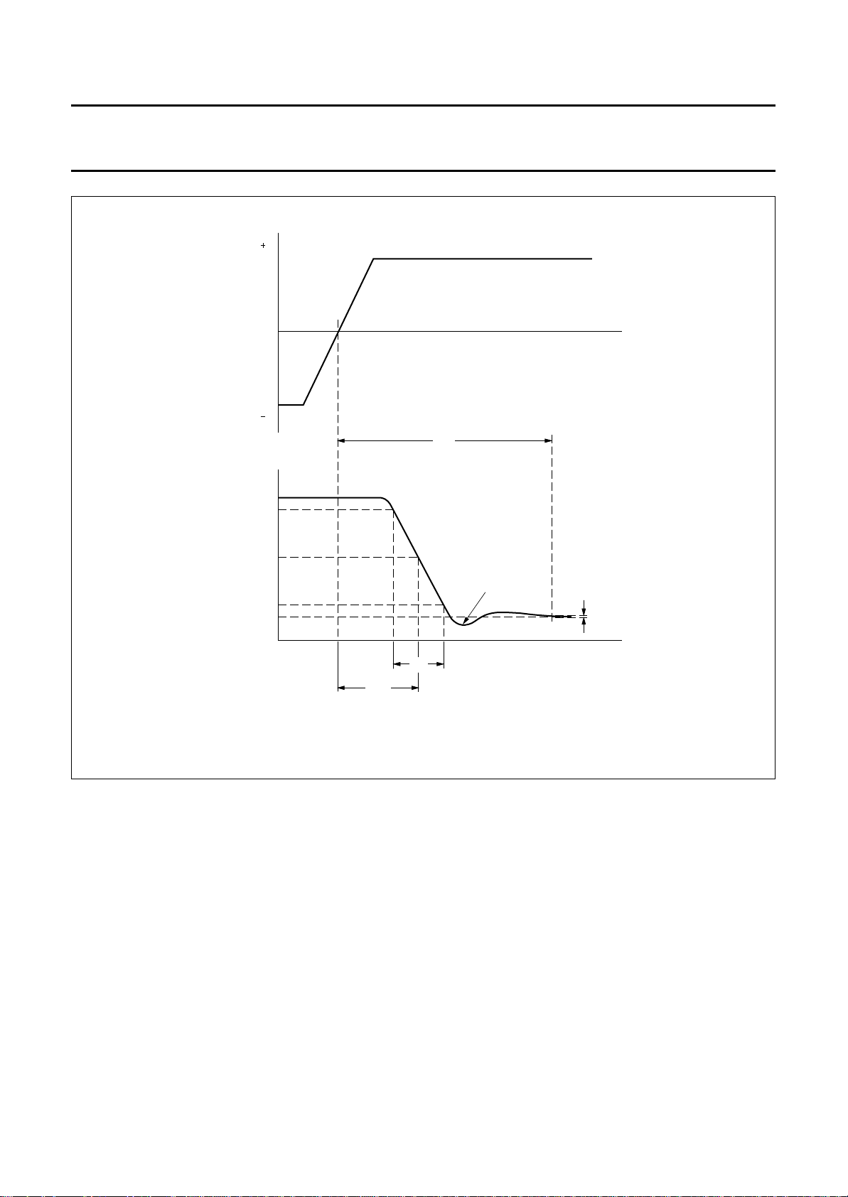
50
t
f
t
pd
t
51
49
t
MGA975
Fig.5 Output voltage (pins 8) falling edge as a function of the AC input signal.
1995 Feb 07 10
Page 11

Philips Semiconductors Preliminary specification
Video output amplifier TDA6101Q
TEST AND APPLICATION INFORMATION
Dissipation
Regarding dissipation, distinction must first be made
between static dissipation (independent of frequency) and
dynamic dissipation (proportional to frequency).
The static dissipation of the TDA6101Q is due to high and
low voltage supply currents and load currents in the
feedback network and CRT.
The static dissipation equals:
×–×+
fb
×+×=
V
-------R
fb
fb
P
stat
V
DDLIDDLVDDHIDDH
VocIocV
= value of feedback resistor.
R
fb
Ioc= DC value of cathode current.
The dynamic dissipation equals:
P
dyn=VDDH
× (CL+Cfb+C
) × fi× V
int
o(p-p)
×δ
CL= load capacitance.
Cfb= feedback capacitance (≈ 150 fF).
C
= internal load capacitance (≈ 4 pF).
int
fi= input frequency.
V
= output voltage (peak-to-peak value).
o(p-p)
δ = non-blanking duty-cycle (≈ 0.8).
The IC must be mounted on the picture tube base print to
minimize the load capacitance (C
).
L
1995 Feb 07 11
Page 12
Philips Semiconductors Preliminary specification
Video output amplifier TDA6101Q
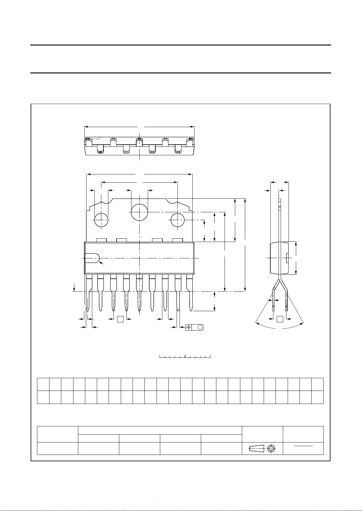
PACKAGE OUTLINE
DBS9MPF: plastic DIL-bent-SIL medium power package with fin; 9 leads
D
D
1
q
P
pin 1 index
P
1
q
2
q
1
SOT111-1
A
2
Q
A
3
A
A
4
E
seating plane
19
Z
b
e
2
b
b
1
0 5 10 mm
scale
DIMENSIONS (mm are the original dimensions)
A
UNIT A A
mm
2
max. max.
18.5
3.7
17.8
8.7
8.0
b
bcD
A
3
4
15.5
1.40
15.1
1.14
b
1
2
0.67
1.40
0.50
1.14
0.48
0.38
(1)
21.8
21.4
(1)
D
E
12
21.4
6.48
20.7
6.20
Note
1. Plastic or metal protrusions of 0.25 mm maximum per side are not included.
OUTLINE
VERSION
IEC JEDEC EIAJ
REFERENCES
SOT111-1
L
w
M
eLPP
2.54
e
2.54
3.9
3.4
2.75
2.50
1
3.4
3.2
Q
1.75
1.55
c
q
q
1
15.1
4.4
14.9
4.2
EUROPEAN
PROJECTION
e
2
θ
q
w
2
5.9
0.25
5.7
ISSUE DATE
92-11-17
95-03-11
Z
1.0
(1)
θ
o
65
o
55
1995 Feb 07 12
Page 13

Philips Semiconductors Preliminary specification
Video output amplifier TDA6101Q
SOLDERING
Plastic single in-line packages
Y DIP OR WAVE
B
The maximum permissible temperature of the solder is
260 °C; this temperature must not be in contact with the
joint for more than 5 s. The total contact time of successive
solder waves must not exceed 5 s.
The device may be mounted up to the seating plane, but
the temperature of the plastic body must not exceed the
specified storage maximum. If the printed-circuit board has
been pre-heated, forced cooling may be necessary
immediately after soldering to keep the temperature within
the permissible limit.
DEFINITIONS
Data sheet status
Objective specification This data sheet contains target or goal specifications for product development.
Preliminary specification This data sheet contains preliminary data; supplementary data may be published later.
Product specification This data sheet contains final product specifications.
Limiting values
Limiting values given are in accordance with the Absolute Maximum Rating System (IEC 134). Stress above one or
more of the limiting values may cause permanent damage to the device. These are stress ratings only and operation
of the device at these or at any other conditions above those given in the Characteristics sections of the specification
is not implied. Exposure to limiting values for extended periods may affect device reliability.
R
EPAIRING SOLDERED JOINTS
Apply the soldering iron below the seating plane (or not
more than 2 mm above it). If its temperature is below
300 °C, it must not be in contact for more than 10 s; if
between 300 and 400 °C, for not more than 5 s.
Application information
Where application information is given, it is advisory and does not form part of the specification.
LIFE SUPPORT APPLICATIONS
These products are not designed for use in life support appliances, devices, or systems where malfunction of these
products can reasonably be expected to result in personal injury. Philips customers using or selling these products for
use in such applications do so at their own risk and agree to fully indemnify Philips for any damages resulting from such
improper use or sale.
1995 Feb 07 13
 Loading...