

Page 1

INTEGRATED CIRCUITS
DATA SH EET
TDA4866
Full bridge current driven vertical
deflection booster
Product specification
Supersedes data of 1995 Aug 31
File under Integrated Circuits, IC02
1996 Oct 10
Page 2
Philips Semiconductors Product specification
Full bridge current driven vertical
TDA4866
deflection booster
FEATURES
• Fully integrated, few external components
• No additional components in combination with the
deflection controller TDA4850/51/55
• Pre-amplifier with differential high CMRR current mode
inputs
• Low offsets
• High linear sawtooth signal amplification
• High efficient DC-coupled vertical output bridge circuit
• Powerless vertical shift
• High deflection frequency up to 140 Hz
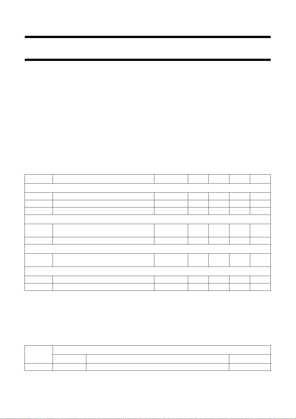
QUICK REFERENCE DATA
SYMBOL PARAMETER CONDITIONS MIN. TYP. MAX. UNIT
DC supply; note 1
V
P
V
FB
I
q
supply voltage (pin 3) 8.2 − 25 V
flyback supply voltage (pin 7) note 2 −−60 V
quiescent current (pin 7) − 710mA
Vertical circuit
I
defl
deflection current
(peak-to-peak value; pins 4 and 6)
I
id
differential input current (peak-to-peak value) note 3 −±500 ±600 µA
Flyback generator
I
FB
maximum current during flyback
(peak-to-peak value; pin 7)
• Power supply and flyback supply voltage independent
adjustable to optimize power consumption and flyback
time
• Excellent transition behaviour during flyback
• Guard circuit for screen protection.
GENERAL DESCRIPTION
The TDA4866 is a power amplifier for use in 90 degree
colour vertical deflection systems for frame frequencies of
50 to 140 Hz. The circuit provides a high CMRR current
driven differential input. Due to the bridge configuration of
the two output stages DC-coupling of the deflection coil is
achieved. In conjunction with TDA4850/51/55 the ICs offer
an extremely advanced system solution.
0.6 − 2A
−−2A
Guard circuit; note 1
V
8
I
8
guard voltage guard on 7.5 8.5 10 V
guard current guard on 5 −−mA
Notes
1. Voltages refer to pin 5 (GND).
2. Up to 60 V ≥ V
≥ 40 V a decoupling capacitor CFB=22µF (between pin 7 and pin 5) and a resistor RFB= 100 Ω
FB
(between pin 7 and VFB) are required (see Fig.4).
3. Differential input current Iid=I1−I2.
ORDERING INFORMATION
TYPE
NUMBER
NAME DESCRIPTION VERSION
PACKAGE
TDA4866 SIL9P plastic single in-line power package; 9 leads SOT131-2
1996 Oct 10 2
Page 3

Philips Semiconductors Product specification
Full bridge current driven vertical
deflection booster
BLOCK DIAGRAM
handbook, full pagewidth
INA 1
INB 2
from e.g.
TDA4850/51/55
TDA4866
INPUT STAGE
GUARD
output
GUARD
CIRCUIT
PROTECTION
TDA4866
V
8
P
GND V
FLYBACK
GENERATOR
AMPLIFIER A
AMPLIFIER B
FB
753
6 OUTA
9
FEEDB
4 OUTB
C
SP
R
SP
R
ref
I
defl
vertical
R
deflection
p
coil
R
m
PINNING
SYMBOL PIN DESCRIPTION
INA 1 input A
INB 2 input B
V
P
3 supply voltage
OUTB 4 output B
GND 5 ground
OUTA 6 output A
V
FB
7 flyback supply voltage
GUARD 8 guard output
FEEDB 9 feedback input
Fig.1 Block diagram.
handbook, halfpage
MED750
INA
1
2
INB
V
3
P
OUTB
4
5
GND
OUTA
V
FB
GUARD
FEEDB
TDA4866
6
7
8
9
MED751
Fig.2 Pin configuration.
1996 Oct 10 3
Page 4

Philips Semiconductors Product specification
Full bridge current driven vertical
deflection booster
FUNCTIONAL DESCRIPTION
The TDA4866 consists of a differential input stage, two
output stages, a flyback generator, a protection circuit for
the output stages and a guard circuit.
Differential input stage
The differential input stage has a high CMRR differential
current mode input (pins 1 and 2) that results in a high
electro-magnetic immunity and is especially suitable for
driver units with differential (e.g. TDA4850/51/55) and
single ended current signals. Driver units with voltage
outputs are simply applicable as well (e.g. two additional
resistors are required).
The differential input stage delivers the driver signals for
the output stages.
Output stages
The two output stages are current driven in opposite phase
and operate in combination with the deflection coil in a full
bridge configuration. Therefore the TDA4866 requires no
external coupling capacitor (e.g. 2200 µF) and operates
with one supply voltage V
flyback supply voltage V
through the coil (I
defl
which produces a voltage drop (Urm) of: Urm≈ Rm× I
At the feedback input (pin 9) a part of I
input stage. The feedback input has a current input
characteristic which holds the differential voltage between
pin 9 and the output pin 4 on zero. Therefore the feedback
current (I
I
9
R
---------R
ref
m
) through R
9
I
×≈
defl
The input stage directly compares the driver currents into
pins 1 and 2 with the feedback current I
this comparison leads to a more or less driver current for
the output stages. The relation between the deflection
current and the differential input current (I
R
I
idI9
---------R
m
ref
I
×≈=
defl
Due to the feedback loop gain (V
bondwire resistance (R
to determine the accurate value of I
and a separate adjustable
P
only. The deflection current
FB
) is measured with the resistor R
is fed back to the
defl
is:
ref
. Any difference of
9
) is:
id
) and internal
U loop
) correction factors are required
bo
:
defl
m
defl
.
TDA4866
R
I
deflIid
with R
for I
≈ 70 mΩ and
bo
1
–
1
---------------- V
Uloop
= 0.7 A.
defl
ref
× 1
-----------------------RmRbo+
0.98≈
×=
The deflection current can be adjusted up to ±1 A by
varying R
when Rm is fixed to 1 Ω.
ref
High bandwidth and excellent transition behaviour is
achieved due to the transimpedance principle this circuit
works with.
Flyback generator
During flyback the flyback generator supplies the output
stage A with the flyback voltage. This makes it possible to
optimize power consumption (supply voltage V
flyback time (flyback voltage VFB). Due to the absence of a
decoupling capacitor the flyback voltage is fully available.
In parallel with the deflection yoke and the damping
resistor (Rp) an additional RC combination (RSP; CSP) is
necessary to achieve an optimized flyback behaviour.
Protection
The output stages are protected against:
• thermal overshoot
• short-circuit of the coil (pins 4 and 6).
Guard circuit
The internal guard circuit provides a blanking signal for the
CRT. The guard signal is active HIGH:
• at thermal overshoot
• when feedback loop is out of range
• during flyback.
The internal guard circuit will not be activated, if the input
signals on pins 1 and 2 delivered from the driver circuit are
out of range or at short-circuit of the coil (pins 4 and 6).
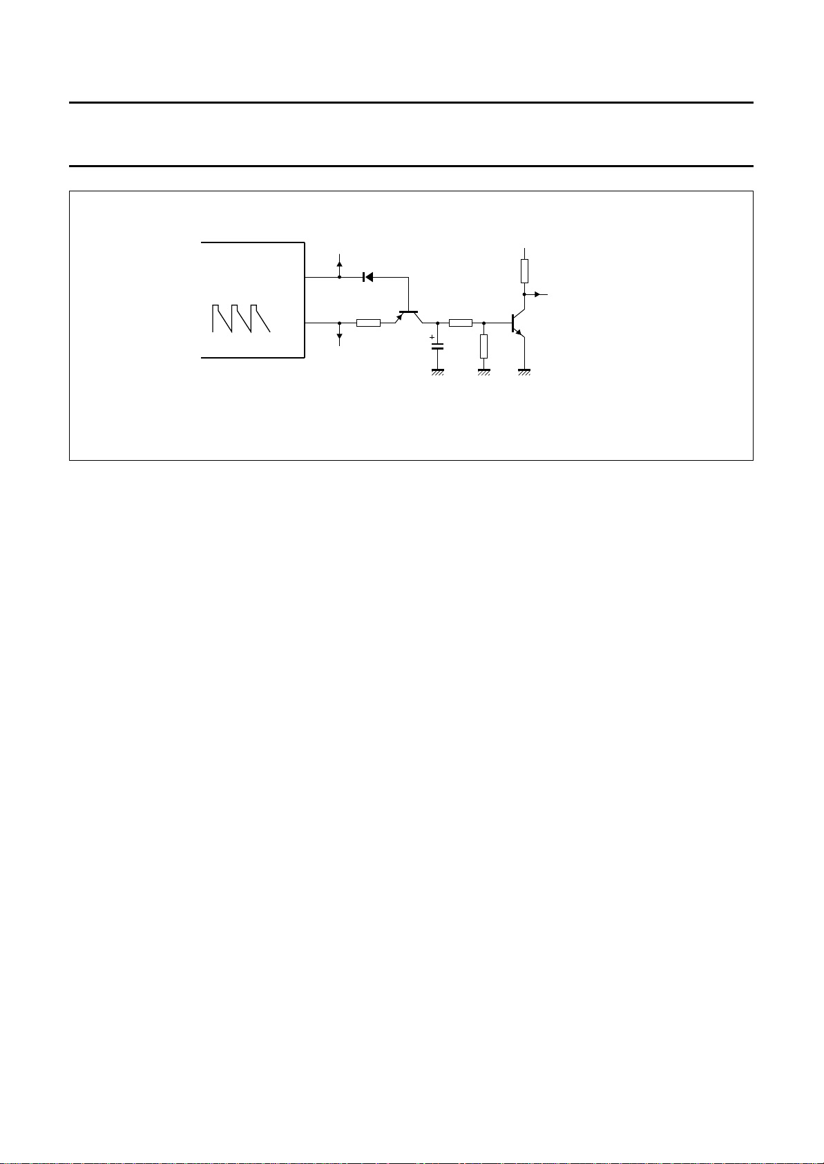
For this reason an external guard circuit can be applied to
detect failures of the deflection (see Fig.6). This circuit will
be activated when flyback pulses are missing, which is the
indication of any abnormal operation.
–
---------------- V
1
Uloop
) and
P
1996 Oct 10 4
Page 5

Philips Semiconductors Product specification
Full bridge current driven vertical
TDA4866
deflection booster
LIMITING VALUES
In accordance with the Absolute Maximum Rating System (IEC 134); voltages referenced to pin 5 (GND); unless
otherwise specified.
SYMBOL PARAMETER MIN. MAX. UNIT
V
P
V
FB
I
FB
V
1,V2
I
1,I2
,V
V
4
6
I
4,I6
V
9
I
9
V
8
I
8
T
stg
T
amb
T
j
V
es
supply voltage (pin 3) 0 30 V
flyback supply voltage (pin 7) 0 60 V
flyback supply current 0 ±1.8 A
input voltage 0 V
P
V
input current 0 ±5mA
output voltage 0 V
P
V
output current (note 1) 0 ±1.8 A
feedback voltage 0 V
P
V
feedback current 0 ±5mA
guard voltage (note 2) 0 VP+ 0.4 V
guard current 0 ±5mA
storage temperature −20 +150 °C
operating ambient temperature −20 +75 °C
junction temperature (note 3) −20 +150 °C
electrostatic handling for all pins (note 4) −500 +500 V
Notes
1. Maximum output currents I
and I6 are limited by current protection.
4
2. For VP> 13 V the guard voltage V8 is limited to 13 V.
3. Internally limited by thermal protection; switching point ≥ 150 °C.
4. Equivalent to discharging a 200 pF capacitor through a 0 Ω series resistor.
THERMAL CHARACTERISTICS
SYMBOL PARAMETER VALUE UNIT
R
th j-mb
thermal resistance from junction to mounting base 4 K/W
1996 Oct 10 5
Page 6

Philips Semiconductors Product specification
Full bridge current driven vertical
TDA4866
deflection booster
CHARACTERISTICS
VP= 15 V; T
(see Fig.3); unless otherwise specified.
SYMBOL PARAMETER CONDITIONS MIN. TYP. MAX. UNIT
V
P
V
FB
I
FB
Input stage
I
id(p-p)
I
1, 2(p-p)
CMRR common mode rejection ratio note 3 −−54 − dB
V
1
V
2
TC
i,1
TC
i,2
− V
V
1
2
I
9
V
9
I
id(offset)
C
i INA
C
i INB
Output stages A and B
I
4
I
6
V
6
V
6,3
V
4
V
4,3
LE linearity error I
V
4
V
6
G
oi
G
ofb
G
ifb
=25°C; VFB= 40 V; voltages referenced to pin 5 (GND); parameters are measured in test circuit
amb
supply voltage (pin 3) 8.2 − 25 V
flyback supply voltage (pin 7) note 1 VP+6 − 60 V
quiescent feedback current (pin 7) no load; no signal − 710mA
differential input current (Iid=I1−I2)
−±500 ±600 µA
(peak-to-peak value)
single ended input current
note 2 0 ±300 ±600 µA
(peak-to-peak value)
input clamp voltage I1= 300 µA 2.7 3.0 3.3 V
input clamp voltage I2= 300 µA 2.7 3.0 3.3 V
input clamp signal TC on pin 1 0 −±800 µV/K
input clamp signal TC on pin 2 0 −±800 µV/K
differential input voltage Iid=0 0 −±10 mV
feedback current −±500 ±600 µA
feedback voltage 1 − VP− 1V
differential input offset current
(I
id(offset)=I1−I2
)
I
= 0; R
defl
Rm=1Ω
= 1.5 kΩ;
ref
0 −±20 µA
input capacity pin 1 referenced to GND −−5pF
input capacity pin 2 referenced to GND −−5pF
output current −−±1A
output current −−±1A
output A saturation voltage to GND I6= 0.7 A − 1.3 1.5 V
= 1.0 A − 1.6 1.8 V
I
6
output A saturation voltage to V
P
I6= 0.7 A − 2.3 2.9 V
= 1.0 A − 2.7 3.3 V
I
6
output B saturation voltage to GND I4= 0.7 A − 1.3 1.5 V
= 1.0 A − 1.6 1.8 V
I
4
output B saturation voltage to V
P
I4= 0.7 A − 1.0 1.6 V
= 1.0 A − 1.3 1.9 V
I
4
= ±0.7 A; note 4 −−2%
defl
DC output voltage Iid= 0 A; closed loop 6.6 7.2 7.8 V
DC output voltage Iid= 0 A; closed loop 6.6 7.2 7.8 V
open loop current gain (I
open loop current gain (I
)I
4, 6/Iid
)I
4, 6/I9
< 100 mA; note 5 − 100 − dB
4, 6
< 100 mA; note 5 − 100 − dB
4, 6
current ratio (Iid/I9) closed loop −−0.2 − dB
1996 Oct 10 6
Page 7

Philips Semiconductors Product specification
Full bridge current driven vertical
TDA4866
deflection booster
SYMBOL PARAMETER CONDITIONS MIN. TYP. MAX. UNIT
I
defl(ripple)
output ripple current as a function of
supply ripple
Flyback generator
V
7, 6
voltage drop during flyback
reverse I
forward I
V
6
V
6
I
7
switching on threshold voltage VP− 1 − VP+ 1.5 V
switching off threshold voltage VP− 1.5 − VP+1 V
flyback current during flyback −−±1A
Guard circuit
V
8
V
8
I
8
V
8
I
8
V
8(ext.)
output voltage guard on 7.5 8.5 10 V
output voltage guard on; VP= 8.2 V 6.9 − VP− 0.4 V
output current guard on 5 −−mA
output voltage guard off −−0.4 V
output current guard off; V8= 5 V 0.5 1 1.5 mA
allowable external voltage on pin 8 0 − 13 V
Notes to the characteristics
1. Up to 60 V ≥ VFB≥ 40 V a decoupling capacitor CFB=22µF (between pins 7 and 5) and a resistor RFB= 100 Ω
(between pin 7 and VFB) are required (see Fig.4).
2. Saturation voltages of output stages A and B can be increased in the event of negative input currents I
deflc
I
idc
I
id
×=
-------- I
defl
= common mode deflection current and I
deflc
3. with I
I
D
---------- -
i
4. Deviation of the output slope at a constant input slope.
5. Frequency behaviour of Goi and G
ofb
:
a) −3 dB open-loop bandwidth (−45°) at 15 kHz; second pole (−135°) at 1.3 MHz.
b) open-loop gain at second pole (−135°) 55 dB.
V
P(ripple)
= ±0.5 V;
−±1−mA
Iid= 0; closed loop
= 0.7 A −−2.0 −3.0 V
defl
= 1.0 A −−2.3 −3.5 V
I
defl
= 0.7 A − +5.6 +6.1 V
defl
= 1.0 A − +5.9 +6.5 V
I
defl
≤ 13 V 0 − VP+ 0.3 V
V
P
= common mode input current.
idc
< −500 µA.
1, 2
1996 Oct 10 7
Page 8
Philips Semiconductors Product specification
Full bridge current driven vertical
deflection booster
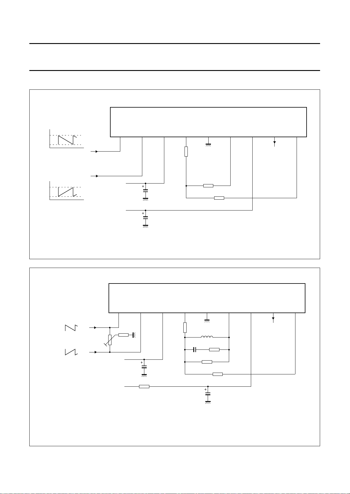
TEST AND APPLICATION INFORMATION
dbook, full pagewidth
I
1
(µA)
550
50
from driver circuit
TDA4850/51/55
I
1
(µA)
550
50
t
I
1
I
2
t
V
P
V
FB
R
1 Ω
TDA4866
TDA4866
4321
m
56789
GUARD
output
6 Ω
R
ref
2 kΩ
MED752
Fig.3 Test diagram.
book, full pagewidth
TDA4866
4321
R
m
I
1
from driver circuit
TDA4850/51/55
(1) Up to 60 V ≥ VFB≥ 40 V RFB= 100 Ω and CFB=22µF are required.
(2) CSP= 10 to 330 nF and RSP=10to22Ω are required. The value of CSP depends on minimum t
V
shift
I
2
25 kΩ
10 kΩ
V
V
FB
P
220 µF
R
FB
(1)
1 Ω
L
deflcoil
R
deflcoil
C
SP
(2)
180 Ω
(1)
56789
= 5.2 mH
= 4.2 Ω
R
SP
(2)
R
p
R
ref
1.6 kΩ
C
FB
100 µF (VFB < 40 V)
flb/VFB
.
GUARD
output
MED753
1996 Oct 10 8
Fig.4 Application diagram with driver circuit TDA4850/51/55.
Page 9
Philips Semiconductors Product specification
Full bridge current driven vertical
deflection booster
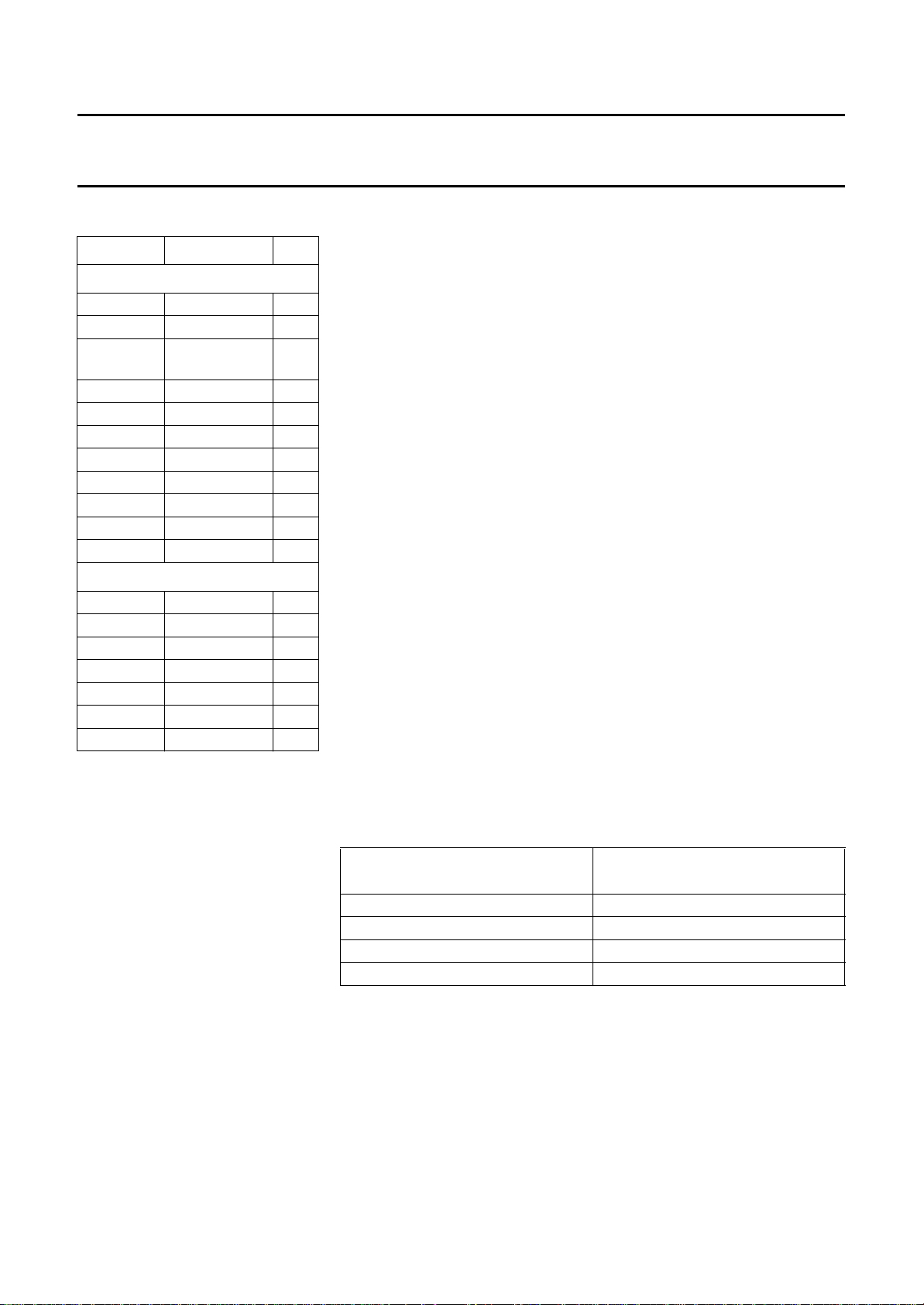
Example
SYMBOL VALUE UNIT
Values given from application
I
defl(max)
L
deflcoil
R
deflcoil
0.71 A
5.2 mH
5.4 [= 4.2 +
Ω
7% + ∆R(ϑ)]
R
m
R
p
R
ref
V
FB
T
amb
T
deflcoil
R
th j-mb
R
th mb-amb
1 (+1%) Ω
180 Ω
1.6 kΩ
35 V
+50 °C
+75 °C
4 K/W
(1)
8 K/W
Calculated values
V
P
t
flb
P
tot
P
defl
P
IC
R
T
j(max)
th tot
(2)
8.6 V
270 µs
3.65 W
0.9 W
2.75 W
12 K/W
+83 °C
Notes
1. A layer of silicon grease between
the mounting base and the
heatsink optimizes thermal
resistance.
2. T
j(max)=PIC
× (R
th j-mb
+ R
th mb-amb
)+T
amb
Calculation formula for supply voltage and power consumption
Vb1=V
Vb2=V6+R
for Vb1>Vb2:VP=V
for Vb2>Vb1:VP=V
with:
U’L=L
fv= vertical deflection frequency.
P
tot
P
defl
P
IC
P
IC
P
defl
P
tot
Calculation formula for flyback time (t
t
flb
with:
t
flb(off)
VFB, I
To achieve good noise suppression the following values for Rp are
recommended:
Recommended values
6, 3+Rdeflcoil
deflcoil
× 2I
deflcoil
I
defl(max)
V
--------------------
P
2
1
R
-- -
deflcoilRm
3
P
–=
totPdefl
× I
defl(max)
× I
defl(max)
b1
b2
defl(max)
+ 0.03 A 0.1 W VFBIFB×++××=
V
+()I
− U’L+Rm×I
+U’L+Rm×I
× f
v
P
2
×=
defl(max)
defl(max)+V4
defl(max)+V4, 3
= power dissipation of the IC
= power dissipation of the deflection coil
= total power dissipation.
)
flb
L
deflcoil
-------------------------------- R
+
deflcoilRm
R
1
+
-------------------------------------------------------------------
ln×= t
-----------------------------------------------------------------------------
R
1
–
-------------------------------------------------------------------
+()I
deflcoilRm
V
FBV7rV6r
deflcoilRm
V
FB
×
–+
+()I
×
V7fV6f–()–
defl(max)
defl(max)
= flyback switch off time = 50 µs for this application (t
defl(max)
, L
deflcoil
L
deflcoil
and CSP).
(mH)
3 100
6 180
10 240
15 390
TDA4866
+
flb(off)
flb(off)
R
p
(Ω)
depends on
1996 Oct 10 9
Page 10
Philips Semiconductors Product specification
Full bridge current driven vertical
deflection booster
handbook, full pagewidth
I
1
I
2
V
6
V
FB
TDA4866
driver current
from TDA4850/51/55
on pin 1
t
driver current
from TDA4850/51/55
on pin 2
t
output voltage
on pin 6
I
V
V
V
defl
V
P
t
4
P
t
t
8
output voltage
on pin 4
deflection current
through the coil
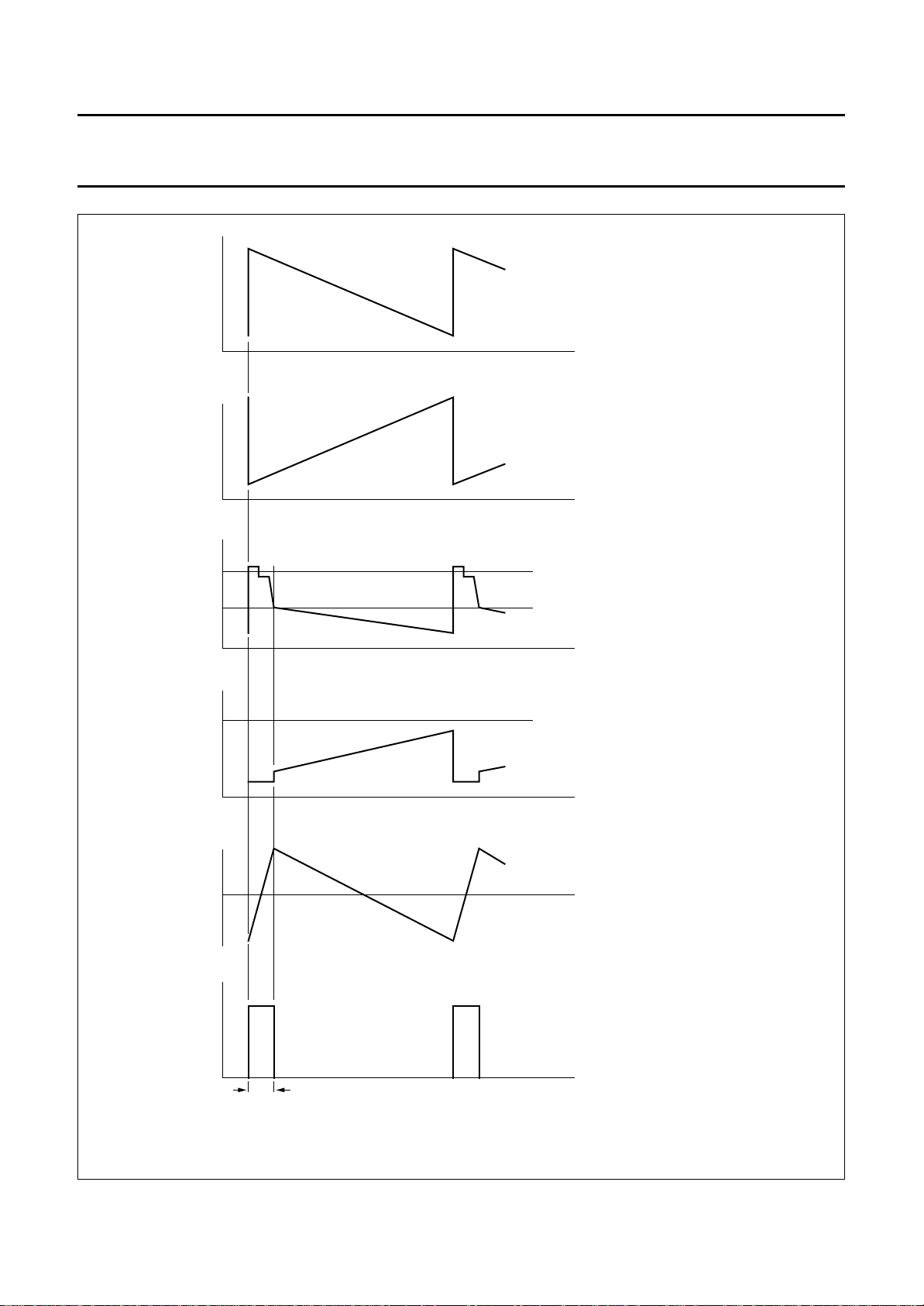
GUARD output voltage
on pin 8
during normal operation
1996 Oct 10 10
t
flb
flyback time t
depends on V
t
flb
FB
MHA062
Fig.5 Timing diagram.
Page 11
Philips Semiconductors Product specification
Full bridge current driven vertical
deflection booster
l pagewidth
TDA4866
Fig.6 Application circuit for external guard signal generation.
7
6
V
FB
vertical
output
signal
BAX13
2.2 Ω
22 µF
2N5819
3.3 kΩ
220
kΩ
2.2
kΩ
V
P
BC548
GUARD output
HIGH = error
MED754
TDA4866
1996 Oct 10 11
Page 12
Philips Semiconductors Product specification
Full bridge current driven vertical
deflection booster
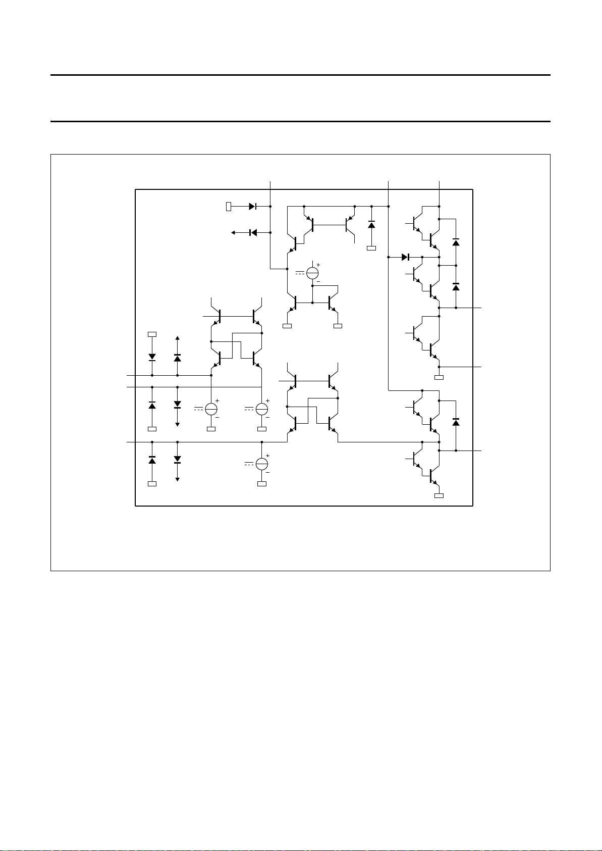
INTERNAL PIN CONFIGURATION
book, full pagewidth
V
P
TDA4866
V
P
2
1
TDA4866
8
3
7
6
5
V
9
P
4
V
P
MED755
Fig.7 Internal circuits.
1996 Oct 10 12
Page 13
Philips Semiconductors Product specification
Full bridge current driven vertical
deflection booster
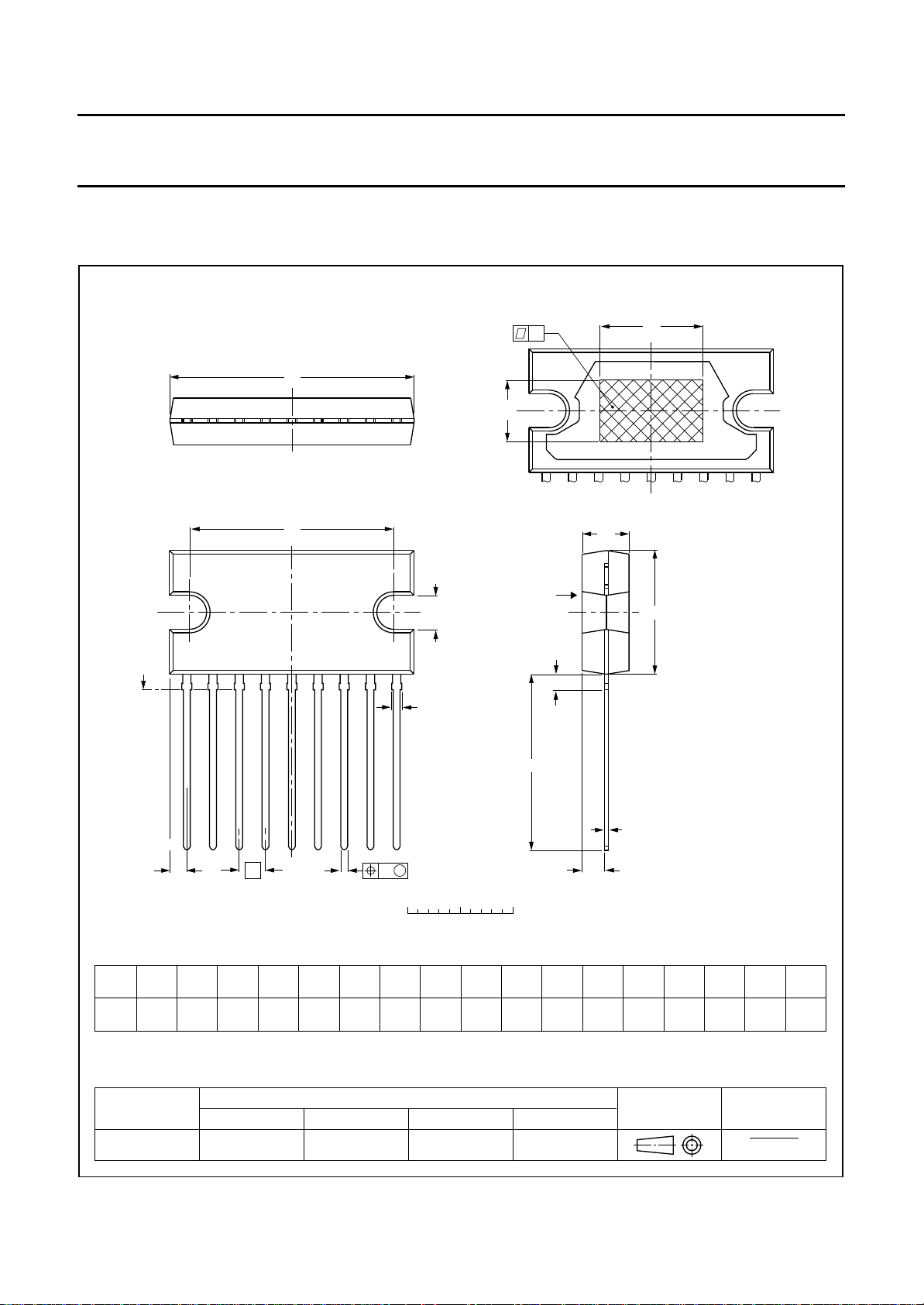
PACKAGE OUTLINE
SIL9P: plastic single in-line power package; 9 leads
D
d
TDA4866
SOT131-2
non-concave
x
E
h
view B: mounting base side
A
B
j
D
h
2
E
seating plane
b
19
Z
DIMENSIONS (mm are the original dimensions)
A
UNIT A
mm
Note
1. Plastic or metal protrusions of 0.25 mm maximum per side are not included.
1
max.
2.0
OUTLINE
VERSION
SOT131-2
4.6
4.2
e
b
b
cD
max.
1.1
p2
0.75
0.48
0.60
0.38
IEC JEDEC EIAJ
b
p
(1)
24.0
23.6
REFERENCES
w M
0 5 10 mm
scale
deD
h
20.0
10 2.54
19.6
E
12.2
11.8
A
1
L
c
Q
(1)
E
h
6
3.4
3.1
Lj
Q
17.2
2.1
16.5
1.8
EUROPEAN
PROJECTION
0.25w0.03
ISSUE DATE
92-11-17
95-03-11
(1)
Z
x
2.00
1.45
1996 Oct 10 13
Page 14

Philips Semiconductors Product specification
Full bridge current driven vertical
TDA4866
deflection booster
SOLDERING
Plastic single in-line packages
Y DIP OR WAVE
B
The maximum permissible temperature of the solder is 260 °C; this temperature must not be in contact with the joint for
more than 5 s. The total contact time of successive solder waves must not exceed 5 s.
The device may be mounted up to the seating plane, but the temperature of the plastic body must not exceed the
specified storage maximum. If the printed-circuit board has been pre-heated, forced cooling may be necessary
immediately after soldering to keep the temperature within the permissible limit.
EPAIRING SOLDERED JOINTS
R
Apply the soldering iron below the seating plane (or not more than 2 mm above it). If its temperature is below 300 °C, it
must not be in contact for more than 10 s; if between 300 and 400 °C, for not more than 5 s.
DEFINITIONS
Data sheet status
Objective specification This data sheet contains target or goal specifications for product development.
Preliminary specification This data sheet contains preliminary data; supplementary data may be published later.
Product specification This data sheet contains final product specifications.
Limiting values
Limiting values given are in accordance with the Absolute Maximum Rating System (IEC 134). Stress above one or
more of the limiting values may cause permanent damage to the device. These are stress ratings only and operation
of the device at these or at any other conditions above those given in the Characteristics sections of the specification
is not implied. Exposure to limiting values for extended periods may affect device reliability.
Application information
Where application information is given, it is advisory and does not form part of the specification.
LIFE SUPPORT APPLICATIONS
These products are not designed for use in life support appliances, devices, or systems where malfunction of these
products can reasonably be expected to result in personal injury. Philips customers using or selling these products for
use in such applications do so at their own risk and agree to fully indemnify Philips for any damages resulting from such
improper use or sale.
1996 Oct 10 14
 Loading...