

Page 1
Power-Factor Controller (PFC) TDA 4862
IC for High Power Factor
and Active Harmonic Filter
Advanced Information Bipolar IC
Features
• IC for sinusoidal line-current consumption
• Power factor approaching 1
• Controls boost converter as an active
harmonics filter
• Internal start-up with low current consumption
• Zero current detector for discontinuous
operation mode
• High current totem pole gate driver
• Trimmed ± 1.4% internal reference
• Undervoltage lock-out with hysteresis
• Very low start-up current consumption
• Pin compatible to world standard
• Fast overvoltage regulator
• Current sense input with internal low pass filter
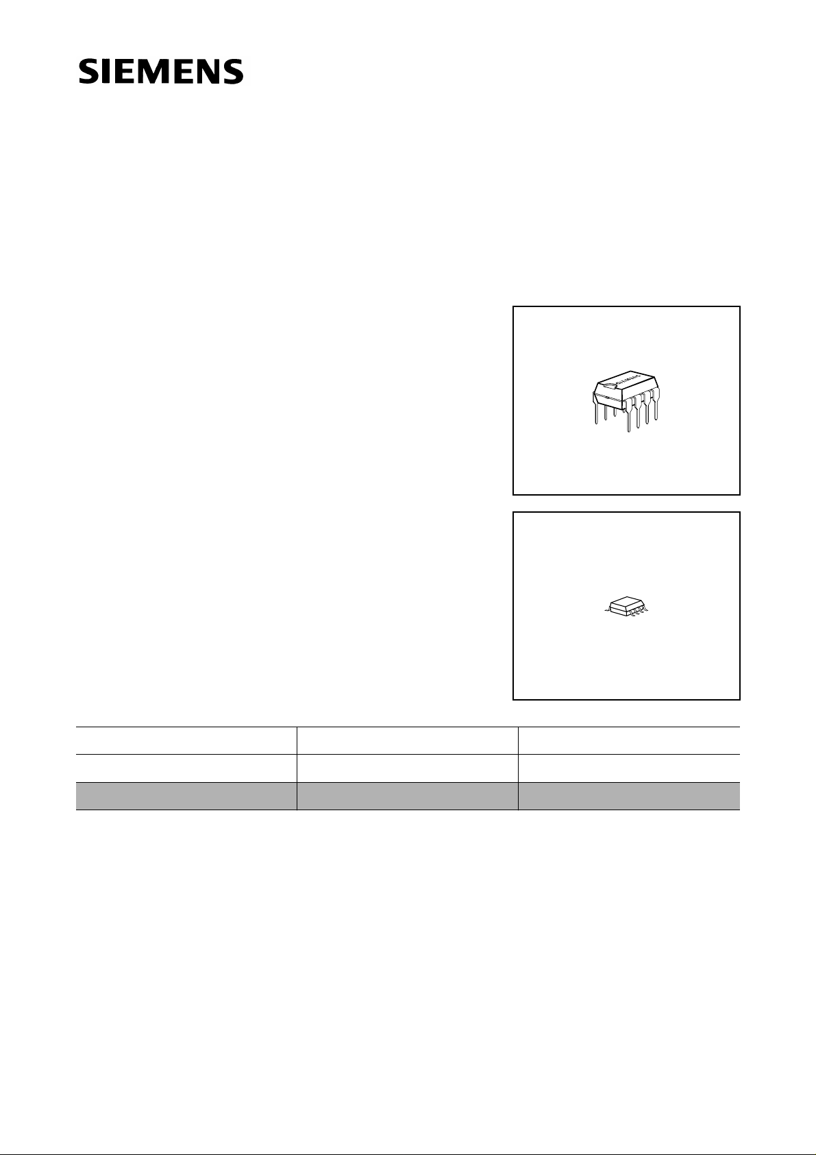
P-DIP-8-1
P-DSO-8-1
Type Ordering Code Package
▼ TDA 4862 Q67000-A8368-A205 P-DIP-8-1
TDA 4862 G Q67006-A8369-A703 P-DSO-8-1
▼
▼ = New type
Semiconductor Group 1 1998-02-16
Page 2
TDA 4862
Description
The TDA 4862 is excellent convenient for designing a preconverter in ballasts and
switched mode power supplies with sinusoidal line current consumption and a power
factor approaching unity.
The TDA 4862 controls a boost converter as an active harmonics filter in a discontinuous
mode (free oscillating triangular shaped current mode).
The TDA 4862 comprises an internal start-up timer, a high gain voltage amplifier, an one
quadrant multiplier for approaching unity power factor, a zero current detector, PWM and
logic circuitry, and totem pole MOSFET gate driver.
V
Protective features are: input undervoltage lockout with hysteresis,
cycle-by-cycle current limiting, output voltage limiting for fast and slow load changes up
to open circuit, and a sinking gate driver current activated whenever undervoltage mode
occurs.
zener clamp,
CC
The output voltage of this preconverter is regulated with high accuracy. Therefore the
device can be used for world-wide line voltages without switches.
The TDA 4862 is the improved version of the TDA 4817 with a pinout equivalent to world
standard.
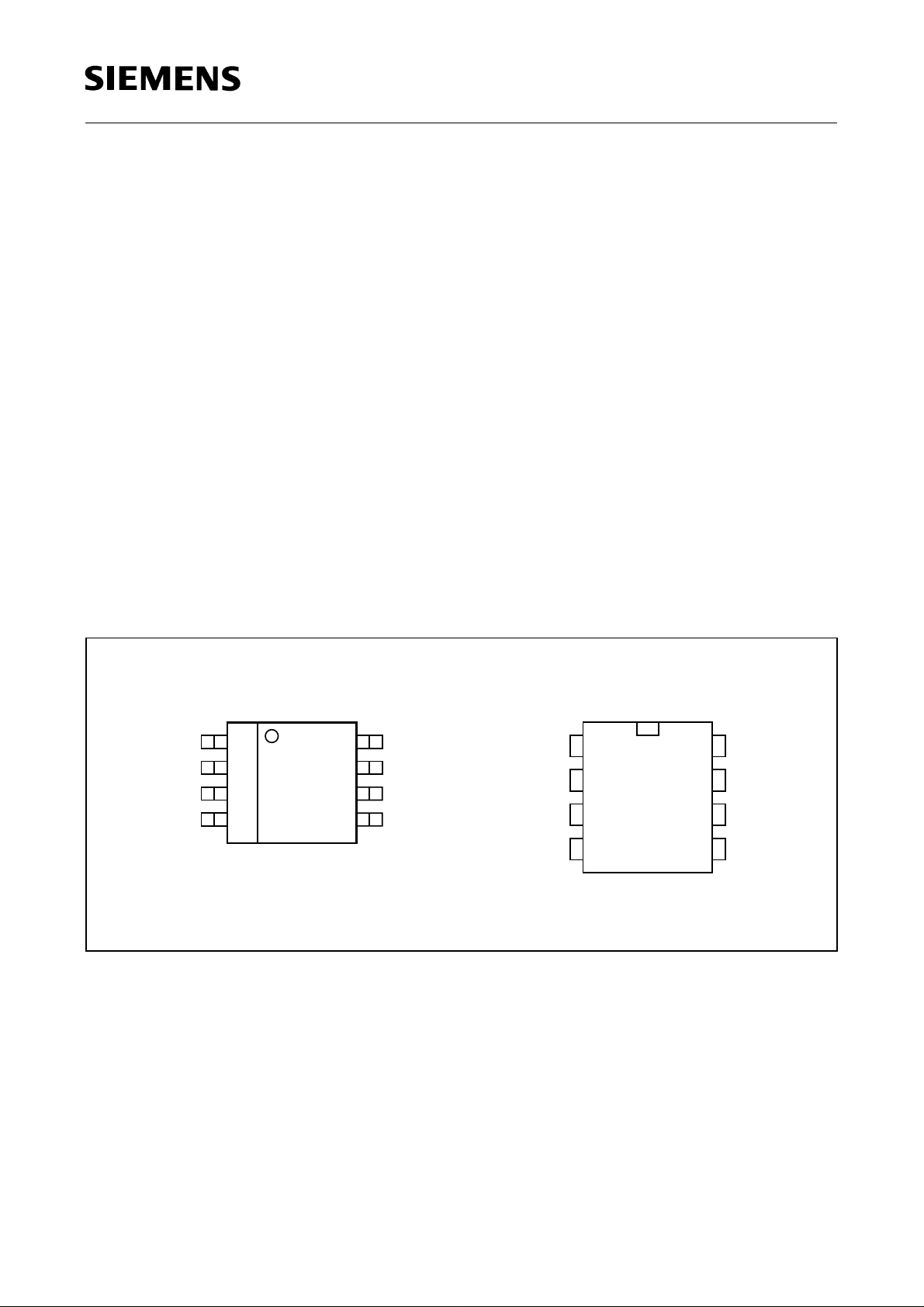
TDA 4862TDA 4862 G
V
SENSE
V
AOUT
MULTIN
Ι
SENSE
1
2
3
4
8
7
6 GND
5
IEP01748
V
CC
GTDRV
DETIN
V
SENSE
V
AOUT
MULTIN
Ι
SENSE
1
2
3
4
8
7
6
5
IEP01749
V
CC
GTDRV
GND
DETIN
Figure 1 Pin Configuration (top view)
Semiconductor Group 2 1998-02-16
Page 3

Pin Definitions and Functions
Pin Symbol Function
1
V
SENSE
Voltage Amplifier Inverting Input;
V
is connected via a resistive divider to the boost converter output.
SENSE
With a capacitor connected to
2
V
AOUT
Voltage Amplifier Output;
V
is connected internally to the first multiplier input. To prevent
AOUT
overshoot the input voltage will be clamped at 5 V. Input voltage less
than 2.2 V is inhibiting the gate driver. If the current flowing into this pin
is exceeding an internal defined margin the multiplier output voltage is
reduced to prevent the MOSFET from overvoltage damage.
3 MULTIN Multiplier Input;
MULTIN is the second multiplier input and connected via a resistive
divider to the rectifier output voltage.
V
it forms an integrator.
AOUT
TDA 4862
4
I
SENSE
Current Sense Minus;
I
is connected to a sense resistor controlling the MOSFET source
SENSE
current. The input is internally clamped at – 0.3 V to prevent negative
input voltage interaction. An internal low pass filter suppresses voltage
spikes when turning the MOSFET on.
5 DETIN Zero Current Detector Input;
DETIN is connected to an auxiliary winding monitoring the zero crossing
of the inductor current.
6 GND Ground;
All voltages are measured with respect to GND.
bypassed directly to GND with a 0.1 µF or larger ceramic capacitor.
7 GTDRV Gate Drive Output;
GTDRV is the output of a totem-pole circuitry for direct driving a
MOSFET. A clamping network bypasses low state source current and
high state sink current.
8
V
CC
Positive Supply Voltage;
V
should be connected to a stable source slightly above the V
CC
turn-ON threshold for normal operation. A 100 nF or lager ceramic
capacitor connected to
V
absorbs supply current spikes required to
CC
charge external MOSFET gate capacitances.
V
should be
CC
CC
Semiconductor Group 3 1998-02-16
Page 4

TDA 4862
Functional Description
Introduction
Conventional electronic ballasts and switching power supplies are designed with a
bridge rectifier and bulk capacitor. Their disadvantage is that the circuit draws power
from the line when the instantaneous AC voltage exceeds the capacitor’s voltage. This
occurs near the line voltage peak and causes a high charge current spike with following
characteristics: the apparent power is higher than the real power that means low power
factor condition, the current spikes are non-sinusoidal with a high content of harmonics
causing line noise, the rectified voltage depends on load condition and requires a large
bulk capacitor, special efforts in noise suppression are necessary.
With the TDA 4862 preconverter a sinusoidal current is achieved which varies in direct
instantaneous proportion to the input voltage half sine wave and means a power factor
near 1. This is due to the appearance of almost any complex load like a resistive one at
the AC line. The harmonic distortions are reduced and comply with the IEC555 standard.
Operating Description
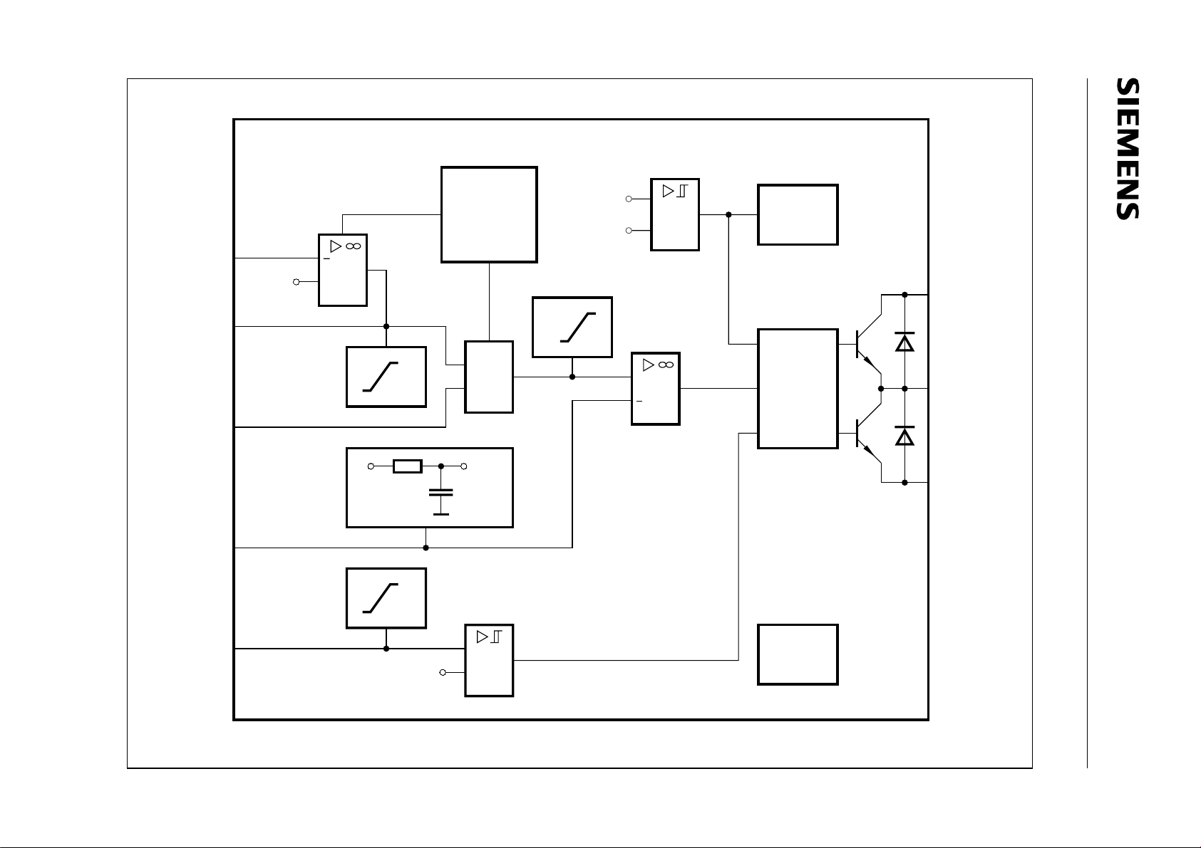
The TDA 4862 contains a wide bandwidth voltage amplifier used in a feedback loop, an
overvoltage regulator, an one quadrant multiplier with a wide linear operating range, a
current sense comparator, zero current detector, a PWM and logic circuitry, a totem-pole
MOSFET driver, an internal trimmed voltage reference, a restart timer and an
undervoltage lockout circuitry. These functional blocks are described below.
Voltage Amplifier
The voltage amplifier is internally compensated and yields a gain bandwidth of 0.8 MHz
and a phase margin of 80 degrees. The non-inverting input is biased at 2.5 V and is not
pinned out. The inverting input is sensing the output voltage via a resitive devider. The
voltage amplifier output
V
and the inverting input V
AOUT
are connected in a simplest
SENSE
way via an external capacitor. It forms an integrator which monitors the average output
voltage over several line cycles. Typically the bandwidth is set below 20 Hz. ln order to
keep the output voltage constant the voltage amplifier output is connected to the
multiplier input for regulation.
Overvoltage Regulator
Fast changes of the output voltage can’t be regulated by the integrator formed with the
voltage amplifier This occurs during initial start-up, sudden load removal, or output
arcing and leads to a current peak at the voltage amplifier input while the voltage
amplifier’s differential input voltages remains zero. The peak current is flowing through
the external capacitor into
V
. Exceeding an internal defined margin causes a
AOUT
regulation circuitry to reduce the multiplier output voltage.
Semiconductor Group 4 1998-02-16
Page 5

TDA 4862
Functional Description (cont’d)
MuItiplier
A one quadrant multiplier is the crucial circuitry that regulates the gate driver with respect
of the DC output voltage and the AC haversine input voltage of the preregulator. Both
inputs are designed for good linearity over a wide dynamic range, 0 V to 4.0 V for the
V
MULTIN and 2.5 V to 4.0 V for the
Current Sense Comparator and RS Latch
The multiplier output voltage is compared with the current sense voltage which
represents the current through the MOSFET. The current sense comparator in addition
with the logic ensures that only a single pulse appears at the drive output during a
given cycle. The multiplier output and the current sense threshold are internally clamped
at 1.3 V. So the gate drive MOSFET is protected against critical operating, as they occur
during start up. To prevent the input from negative pulses a special protection circuitry
is implemented. Switch-on current peaks are reduced by an internal RC-Filter.
AOUT
.
Zero Current Detector
The zero current detector senses the inductor current via an auxiliary winding and
ensures that the next on-time is initiated immediately when the inductor current has
reached zero. This diminishes the reverse recovery losses of the boost converter diode.
Output switch conduction is terminated when the voltage drop of the shunt resistor
reaches the threshold level of the multiplier output. So the boost current waveform has
a triangular shape and there are no deadtime gaps between the cycles. This leads to a
continuous AC line current limiting the peak current to twice of the average current.
To prevent false tripping the zero current detector is designed as a Schmitt trigger with
a hysteresis of 0.6 V. An internal 5 V clamp protects the input from overvoltage
breakdown, a 0.6 V clamp prevents substrate injection. An external resistor must be
used in series with the auxiliary winding to limit the current through the clamps.
Timer
A restart timer function was added to the IC to eliminate the need for an oscillator when
used in stand-alone applications. The timer starts or restarts the TDA 4862 if the drive
output has been off for more than 15 µs after the inductor current reaches zero.
Semiconductor Group 5 1998-02-16
Page 6

Functional Description (cont’d)
Undervoltage Lockout
TDA 4862
An undervoltage lockout circuitry enables the output stage when
threshold
threshold
clamp has been added from
V
and terminates the output stage when VCC is falling below the lower
CC
V
. In the standby mode the supply current is typically 75 µA. An internal
CCL
V
to ground to protect the IC from an overvoltage
CC
condition. The external circuitry is created with a start-up resistor connected from
the input supply voltage and a storage capacitor from
V
to ground. Bootstrap power
CC
V
reaches the upper
CC
V
CC
to
supply is created with the previous mentioned auxiliary winding and a diode.
Output
The TDA 4862 totem pole output stage is MOSFET compatible. An internal protection
V
circuitry is activated when
is within the stand by mode and ensures that the MOSFET
CC
is turned-OFF. The totem pole output has been optimized to minimize cross conduction
current during high speed operation. The addition of two 4 Ω resistors, one in series with
the source output transistor and one in series with the sink output transistor, reduces the
cross conduction current.
Semiconductor Group 6 1998-02-16
Page 7
Semiconductor Group 7 1998-02-16
Figure 2 Block Diagram
V
SENSE
V
AOUT
1
V
2
Voltage
Amplifier
REF
Undervoltage
Lockout
V
Over-
Voltage
11 V / 8.5 V
Regulation
+
Clamp
1.3 V
CC
Current
Reference
Voltage
8
V
CC
Comp
MULTIN
Ι
SENSE
DETIN
Clamp
4 V
0.9 V
3
Ω
Filter
30 k
Multi-
plier
10 pF
+
TDA 4862; G
Driver
and
Logic
7
GTDRV
6
GND
4
5 V
Clamp
0.6 V
5
2.5 V / 1.9 V
Detector
V
CC-
Z-Clamp
TDA 4862
IEB01747
Page 8
Semiconductor Group 8 1998-02-16
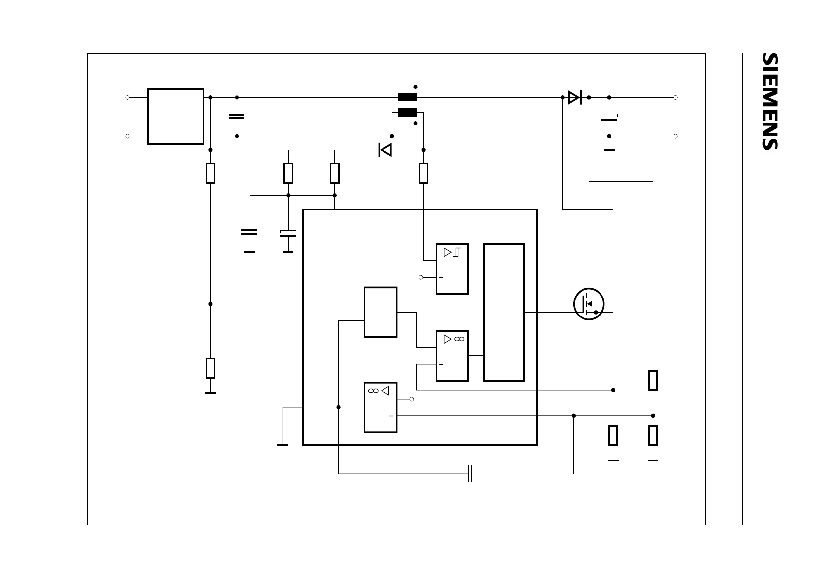
Figure 3 Application Circuit with TDA 4862; G
V
IN
AC
90-270 V
RF-Filter
and
Rectifier
R
1
Ω
1.3 M
C
4
100 nF
R
2
Ω
12 k
C
1
µ
0.22 F
C
3
µ
100 F
MULTIN
R
100 k
GND
µ
250 H
Tr1
BYP 101
D2
C
5
470 F
Ω
R
8
100
3
Ω
D1
1N4148
R
3
22 k
Ω
V
OUT
400 V
µ
DETIN
85
Detector
+
V
TH
Multi-
pler
Current
OP
3
PWM
Logic
Driver
GTDRV
7
Q1
BUZ 334
+
Voltage
OP
+
V
Ref
6
TDA 4862 G
4
1
Ι
SENSE
V
SENSE
R
5
1.6 M
Ω
2
V
AOUT
C
6
470 nF
R
0.1
7
Ω
R
6
Ω
10 k
IES01750
TDA 4862
Page 9
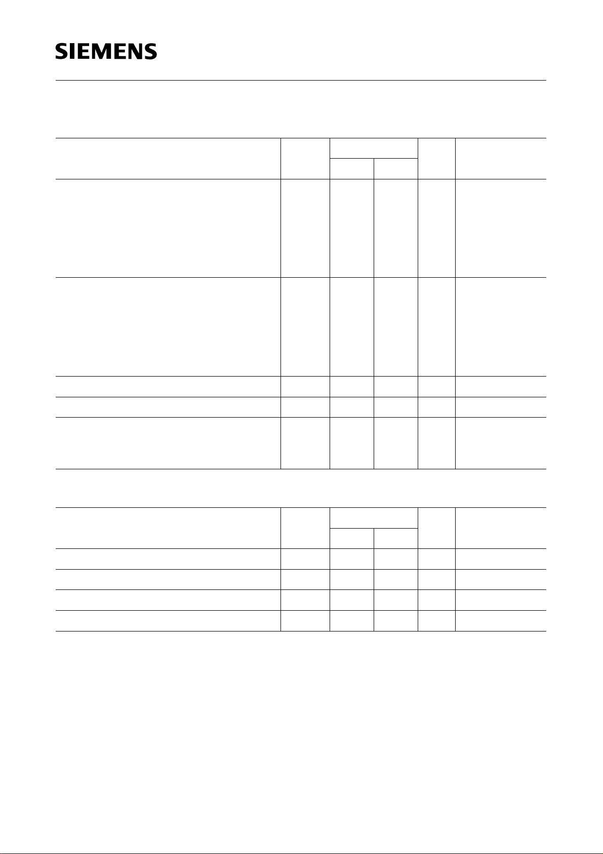
TDA 4862
Absolute Maximum Ratings
Parameter Symbol Limit Values Unit Notes
min. max.
Supply voltage at
supply + Z-current
V
CC
V
-GND Pin 8
CC
Pin 8
Current into GTDRV Pin 7
Clamping current into GTDRV Pin 7
Clamping current into GTDRV Pin 7
Voltage at
Voltage at
V
SENSE
V
AOUT
Pin 1
Pin 2
Voltage at MULTIN Pin 3
Voltage at
I
SENSE
Pin 4
Current into DETIN Pin 5
Current into DETIN Pin 5
Junction temperature
Storage temperature
Thermal resistance system-air
TDA 4862
TDA 4862 G
V
CC
I
CCZ
I
GTDRV
I
GTDCH
I
GTDCL
V
VSENSE
V
VAOUT
V
MULTIN
V
ISENSE
I
DETINH
I
DETINL
T
j
T
stg
R
thSA
R
thSA
– 0.3
0
– 400
–
– 100
– 0.3
– 0.3
– 0.3
–10
–
–10
–
70
500
100
–
17
6
17
17
50
–
V
mA
mA
mA
mA
V
V
V
V
mA
mA
–
observe
observe P
V
GTDRV
V
GTDRV
–
–
–
–
V
DETIN
V
DETIN
– 40 150 °C–
– 50 150 °C–
–
–
100
180
K/W
K/W
P-DIP-8-1
P-DSO-8-1
P
max
max
> V
CC
< – 0.3 V
>6 V
< 0.9 V
Operating Range
Parameter Symbol Limit Values Unit Notes
min. max.
Supply voltage
Z-current I
Junction temperature T
Voltage at
1)
V
CCON
standby to active. For
is in standby and output GTDRV is active low.
I
SENSE
means V
has been exceeded but the supply voltage is still above V
CCH
V
CCH
and V
values see Electrical Characteristics. If 0 V < VCC< V
CCL
V
CC
Z
j
V
ISENSE
V
CCON
V
Z
V
0 50 mA observe P
– 40 150 °C–
– 5 V
Z
V–
. The device has switched from
CCL
1)
CCON
max
, the device
Semiconductor Group 9 1998-02-16
Page 10
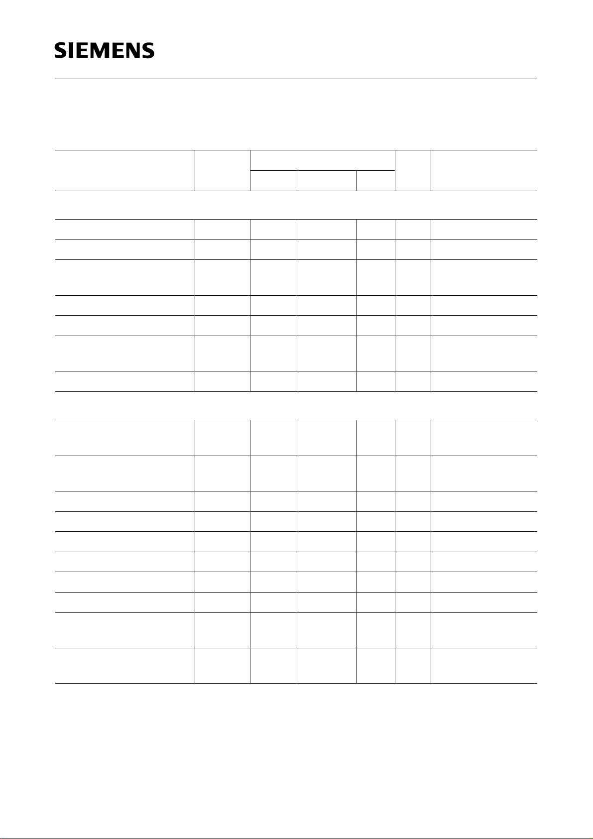
TDA 4862
Electrical Characteristics
V
Unless otherwise stated,
Parameter Symbol Limit Values Unit Test Condition
Overall
= 12 V, – 40 °C < Tj < 150 °C.
CC
min. typ. max.
Supply current, OFF
Supply current, ON I
Supply current, dynamic
V
turn-ON threshold V
CC
V
turn-OFF threshold V
CC
V
turn-ON/OFF
CC
hysteresis
V
clamp V
CC
Voltage Amplifier
Voltage feedback
threshold
Voltage feedback
threshold
Line regulation ∆
I
CCL
CCH
I
CCDY
CCH
CCL
V
CCHY
Z
V
FB
V
FB
V
FBL
– 75 200 µA 0 V < VCC < V
CCH
– 4 6 mA Output low
– 4.2 8 mA f
DETIN
C
GTDRV
= 50 kHz,
= 1 nF
– 11 11.5 V –
8.0 8.5 – V –
1.8 2.3 3.0 V –
15 17 19 V I
= 50 mA
CCZ
2.465 2.5 2.535V Tj= 25 °C,
Pin 1 to Pin 2
2.45 – 2.55 V Pin 1 to Pin 2
–– 5mVVCC = 10 V to 15 V
Input bias current
Open loop voltage gain
Unity gain bandwidth
Phase margin
1)
Inhibit threshold voltage
Output current source
Output current sink
1)
Guaranteed by design, not 100 % tested in production.
Semiconductor Group 10 1998-02-16
I
BVSENSE
1)
G
V
1)
B
W
Φ
M
V
VAOUTI
I
VAOUTH
I
VAOUTL
–1 – – µA–
– 80 – dB –
– 0.8 – MHz –
– 80 – Degr –
– 2.2 – V –
– – 12 – mA V
–4 –mAV
VAOUT
V
VSENSE
VAOUT
V
VSENSE
= 0 V,
= 2.3 V
= 4 V,
= 2.8 V
Page 11
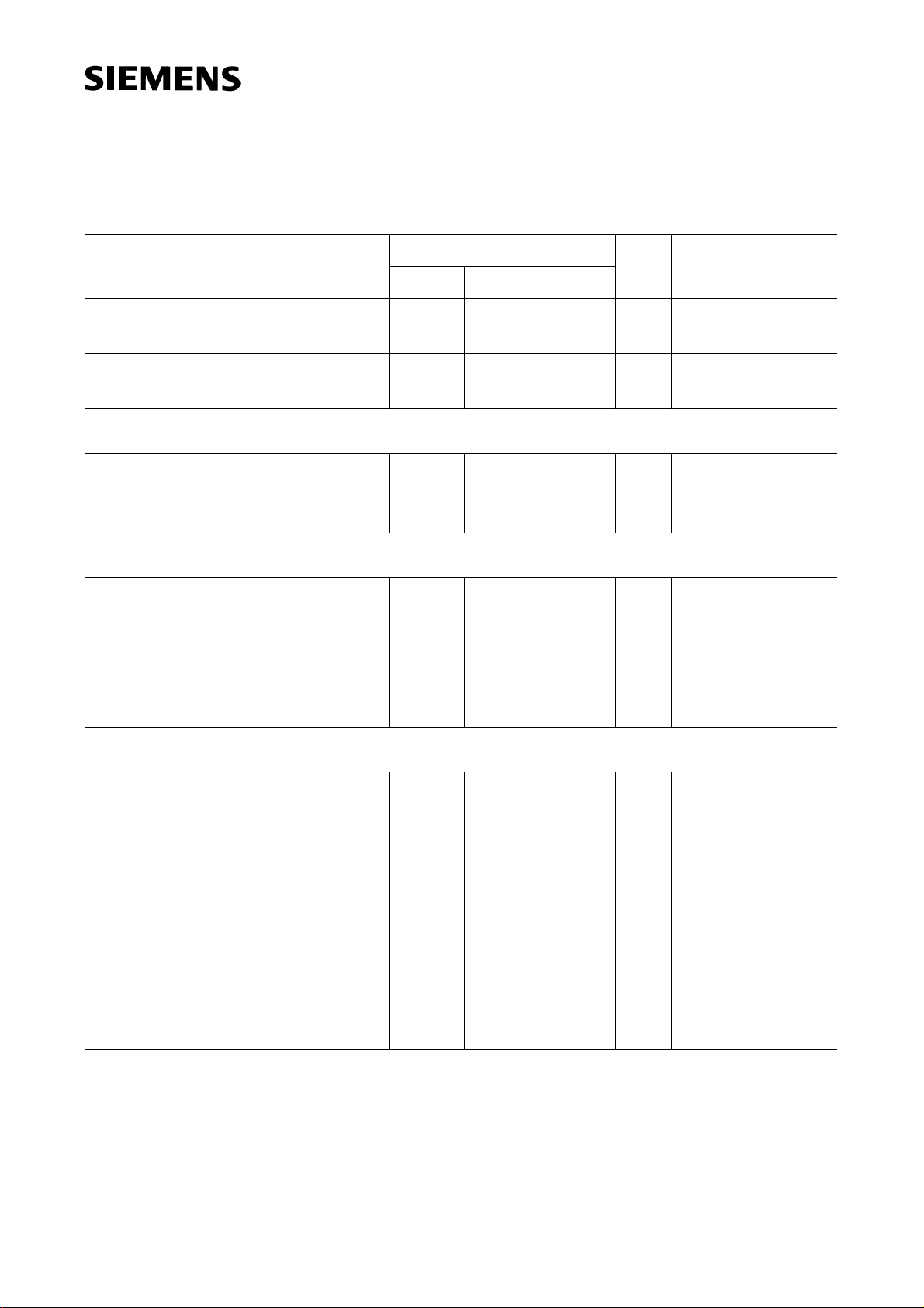
TDA 4862
Electrical Characteristics (cont’d)
V
Unless otherwise stated,
Parameter Symbol Limit Values Unit Test Condition
= 12 V, – 40 °C < Tj < 150 °C.
CC
min. typ. max.
Output voltage swing
high state
Output voltage swing
low state
Overvoltage Regulator
Regulation current
Current Comparator
Input bias current
Input offset voltage
Max threshold voltage
Delay to output
1)
Detector
V
VAOUTH
V
VAOUTL
I
RVAOUT
I
BISENSE
V
ISENSEO
V
ISENSEM
t
PHL
3.8 4.3 5.0 V I
– 0.9 – V I
20 30 45 µA V
VAOUT
V
VSENSE
VAOUT
V
VSENSE
VAOUT
= 4 V,
V
ISENSE
–1 – – µA–
–25 –mVV
MULTIN
V
VAOUT
1.05 1.25 1.5 V –
– 250 – ns –
= – 0.2 mA
= 2.3 V
= 0.5 A
= 2.8 V
=V
MULTIN
= 0.5 V
= 0 V,
= 2.4 V
Upper threshold voltage
(
V
increasing)
DETIN
Lower threshold voltage
(
V
decreasing)
DETIN
Hysteresis
Input current
V
DETINU
V
DETINL
V
DETINHY
I
BDETIN
– 2.5 2.75 V –
1.5 1.9 – V –
– 0.6 – V –
–1 – – µA 1.5 V < V
Input clamp voltage
High state
Low state
1)
Guaranteed by design, not 100 % tested in production.
V
DETINHC
V
DETINLC
4
–
5
0.6
DETIN
< 2.75 V
–
1
V
V
I
DETIN
I
DETIN
= 5 mA
= – 5 mA
Semiconductor Group 11 1998-02-16
Page 12
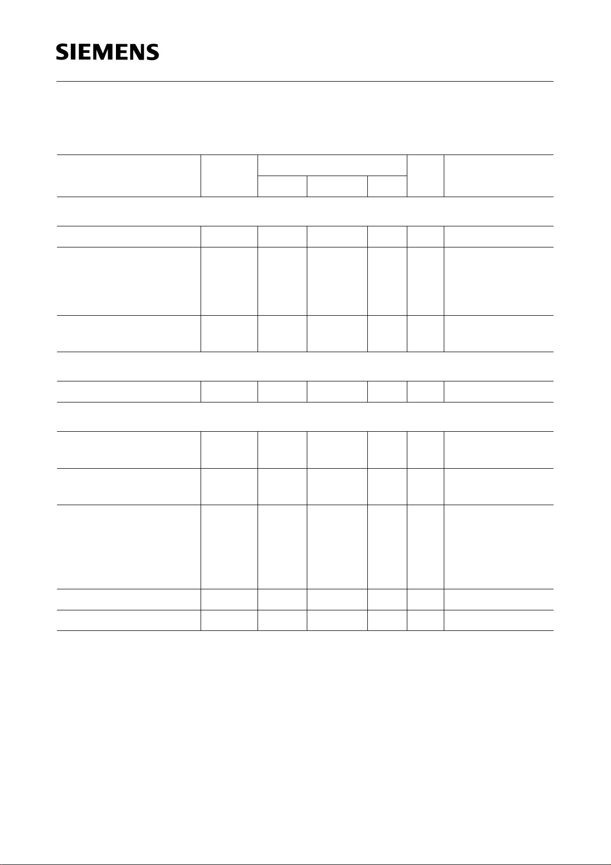
TDA 4862
Electrical Characteristics (cont’d)
V
Unless otherwise stated,
Parameter Symbol Limit Values Unit Test Condition
Multiplier
= 12 V, – 40 °C < Tj < 150 °C.
CC
min. typ. max.
Input bias current
I
BMULTIN
– 1 – – µA–
Dynamic voltage range
MULTIN
V
AOUT
V
MULTIN
V
VAOUT
0 to 3
V
V
2)
2)
/ (V
1)
MULTIN
× (V
K 0.45 0.65 0.85 1/V V
VAOUT
t
DLY
V
GTDRVL
V
GTDRVH
V
GTDRVU
t
r
t
f
– VFB))
75 190 400 µs–
– 0.8
– 9.4
– 2.0 2.6 V I
– 100 – – C
–40 ––C
Multiplier gain
Restart Timer
Restart time delay
Gate Driver
Output voltage low state
Output voltage high
state
Output voltage active
shut down
Rise time
Fall time
1)
K = V
ISENSE
2)
Guaranted by design, not 100% tested in production.
FB
FB
to
+ 1
0 to 4
V
to
FB
V
+ 1.5
FB
1.8
8.7
–
–
V
V
–V
V
–VI
V
V
V
I
GTDRV
I
GTDRV
GTDRV
I
GTDRV
GTDRV
V
0 <
V
0 <
= 2.75 V
VAOUT
MULTIN
MULTIN
= VFB + 1 V
VAOUT
= 20 mA
= 200 mA
= – 20 mA
= – 200 mA
= 50 mA
increasing:
CC
V
CC
decreasing:
CC
V
CC
= 1 nF
GTDRV
= 1 nF
GTDRV
= 1.0 V
= 2 V
< V
CCH
< V
CCL
,
Semiconductor Group 12 1998-02-16
Page 13
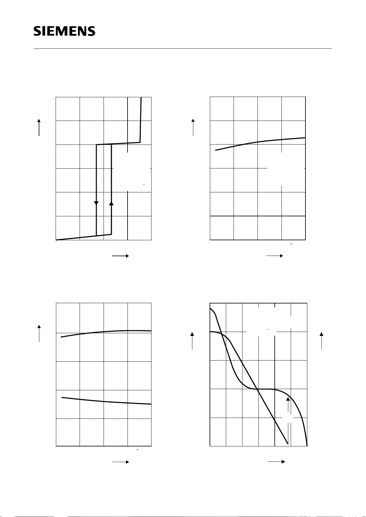
TDA 4862
Supply Current ICC versus
Supply Voltage
6
mA
Ι
CC
5
4
3
2
1
0
0
V
CC
V
VSENSE
V
VAOUT
V
MULTIN
V
ISENSE
V
DETIN
T
j
5
10 15
IED01751
= 3 V
= 3 V
= 1 V
= 0.5 V
= 2 V
= 25 C
V
V
CC
20
Supply Current ICC versus
Junction Temperature
6
mA
Ι
CC
5
4
3
2
1
0
-50
0 50 100
T
j
V
VSENSE
V
VAOUT
V
MULTIN
V
ISENSE
V
DETIN
IED01752
= 3 V
= 3 V
= 1 V
= 0.5 V
= 2 V
150
C
T
j
Turn-ON/-OFF Threshold Voltage V
versus Junction Temperature T
12
V
V
CC
11
10
9
8
7
-50
0 50 100
V
V
CCH
CCL
T
j
IED01753
150
C
j
CC
Open Loop Gain GV and Phase Φ
versus Frequency
100
dB
G
V
80
A
60
Φ
40
20
0
10
-1
-2 1
10
0
10
V
3.0 <
T
0
f
= 12 V
CC
V
VAOUT
= 25 C
j
10 10
10
< 3.5 V
Φ
2
kHz
f
IED01754
M
0
deg
30
60
90
120
150
4
Φ
Semiconductor Group 13 1998-02-16
Page 14
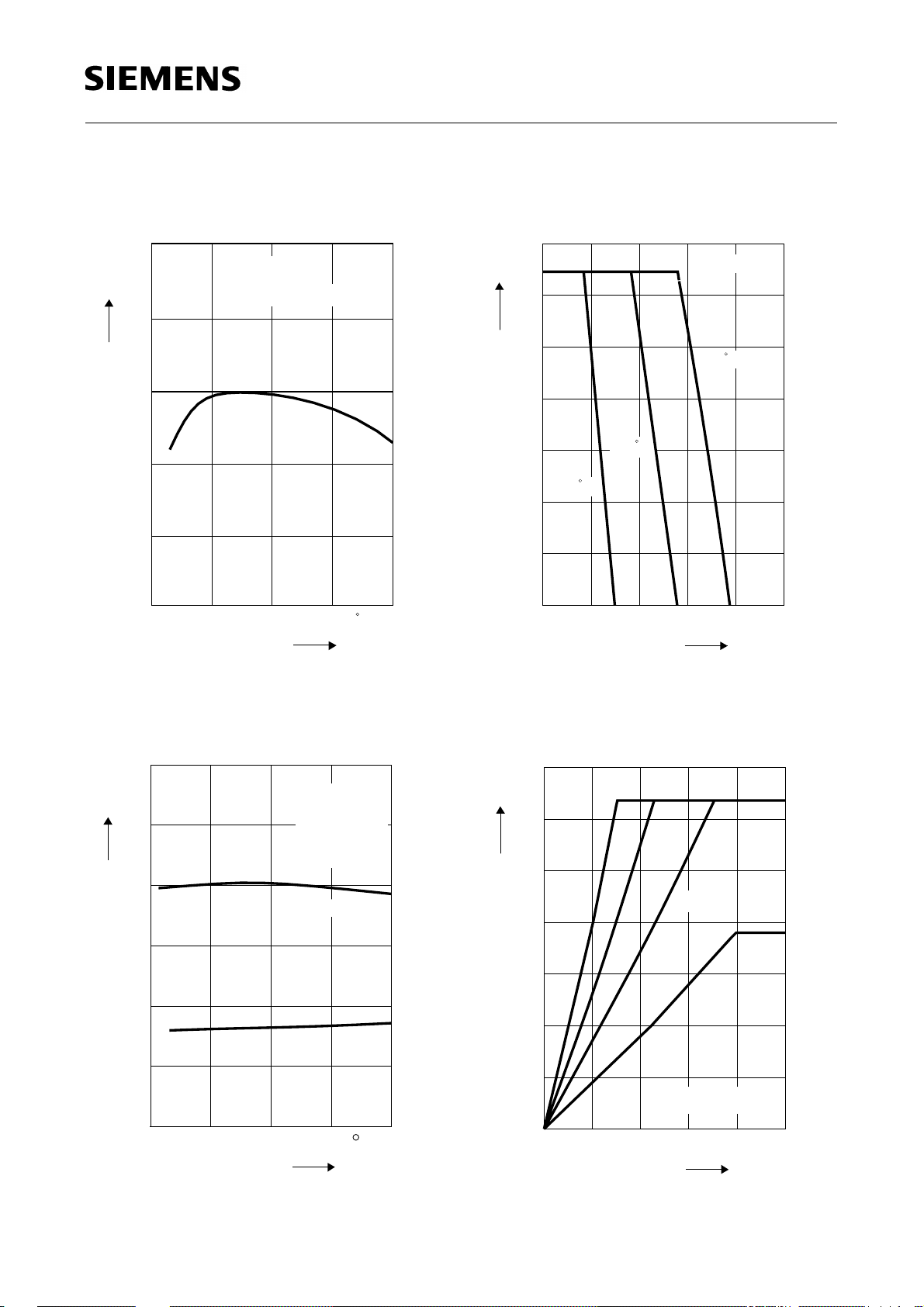
TDA 4862
Threshold Voltage Change ∆VFB versus
Junction Temperature
10
mV
∆
V
FB
5
0
-5
-10
-15
-50
= 12 V
V
CC
Pin 1 connected to Pin 2
0 50 100
T
j
IED01755
150
C
T
j
Threshold Voltage V
Regulation Current
1.4
V
ISENSE
V
1.0
0.8
0.6
150 C
0.4
0.2
0
29
25 C
ISENSE
I
RVAOUT
323130
versus
IED01756
V
=12 V
CC
-40 C
33
µ
Ι
RVAOUT
34
A
Threshold Voltage V
DETIN
Junction Temperature
3.00
1/V
V
DETIN
2.75
2.50
V
2.25
2.00
V
1.75
0
-50
0 50 100
versus
T
j
V
CC
V
MULTIN
V
VSENSE
V
ISENSE
DETINupper
DETINlow
IED01757
= 12 V
= 1 V
= GND
= GND
150
C
T
j
Current Sense Threshold V
Multiplier Input
1.4
V
ISENSE
V
1.0
0.8
0.6
0.4
0.2
0
0
V
4.0 V
MULTIN
3.5 V
V
VAOUT
21
3.0 V
2.75 V
= 2.5 V
3
ISENSE
IED01758
4
V
MULTIN
versus
5
V
Semiconductor Group 14 1998-02-16
Page 15
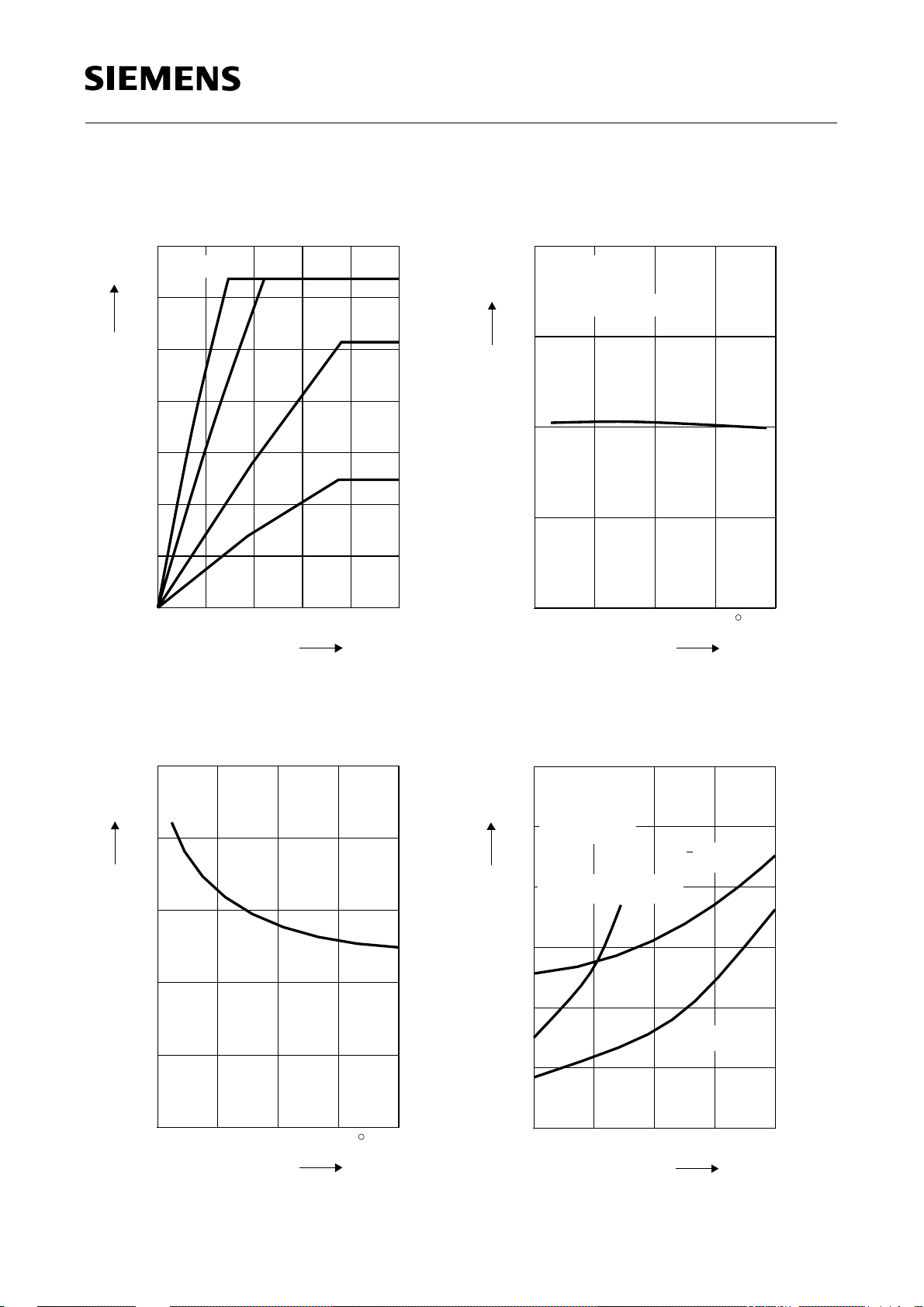
TDA 4862
Current Sense Threshold V
Voltage Amplifier Output
1.4
V
ISENSE
V
V
1.0
0.8
0.6
0.4
0.2
0
2.5
MULTIN
= 3 V
3.53.0
2 V
4.0
ISENSE
V
VAOUT
1 V
4.5
versus
IED01759
0.5 V
V
V
VAOUT
5.0
Multiplier Gain K versus
Junction Temperature
1.2
V
1/V
K
V
V
0.9
0.6
0.3
0
-50
= 12 V
CC
= 2 V
MULTIN
= VFB + 1 V
VAOUT
0 50 100
T
j
IED01760
150
C
T
j
Restart Time Delay t
DLY
Junction Temperature
240
s
µ
t
DLY
220
200
180
160
140
-50
0 50 100
versus
T
j
IED01761
T
Output Voltage Low/High State V
versus Load Current I
6
V
= 12 V
CC
V
V
SAT
5
4
T
= 10 ms
t
= 200 s
p
V
GTDRVL
at
µ
V
CC
GTDRV
VV
CC
GTDRVH
= 7 V
IED01762
SAT
3
2
V
GTDRVL
1
0
150
C
j
0
100 200
300
mA
Ι
GTDRV
400
Semiconductor Group 15 1998-02-16
Page 16
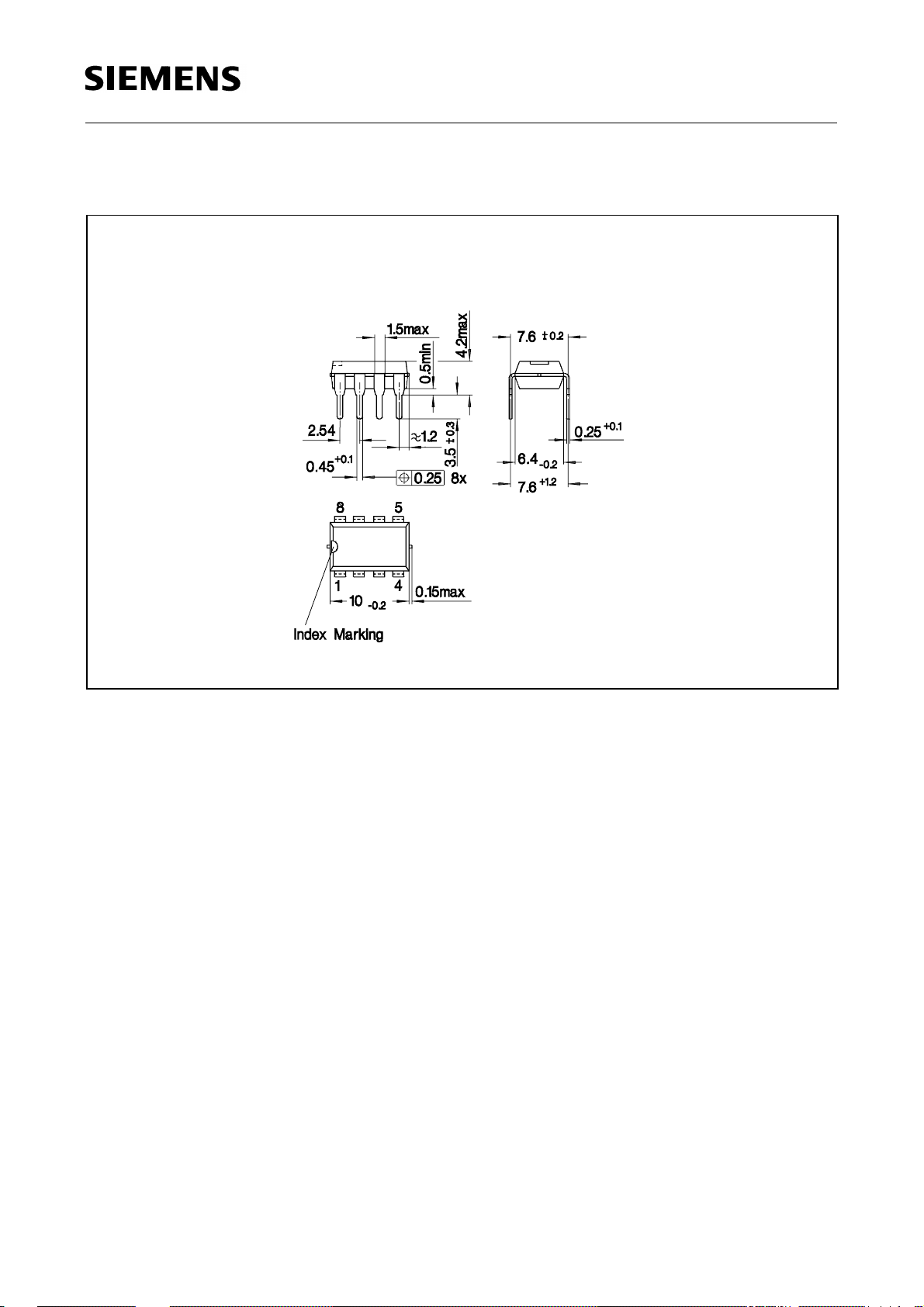
Package Outlines
Plastic Package, P-DIP-8-1
(Plastic Dual In-line Package)
TDA 4862
GPD05025
Sorts of Packing
Package outlines for tubes, trays etc. are contained in our
Data Book “Package Information”.
Dimensions in mm
Semiconductor Group 16 1998-02-16
Page 17
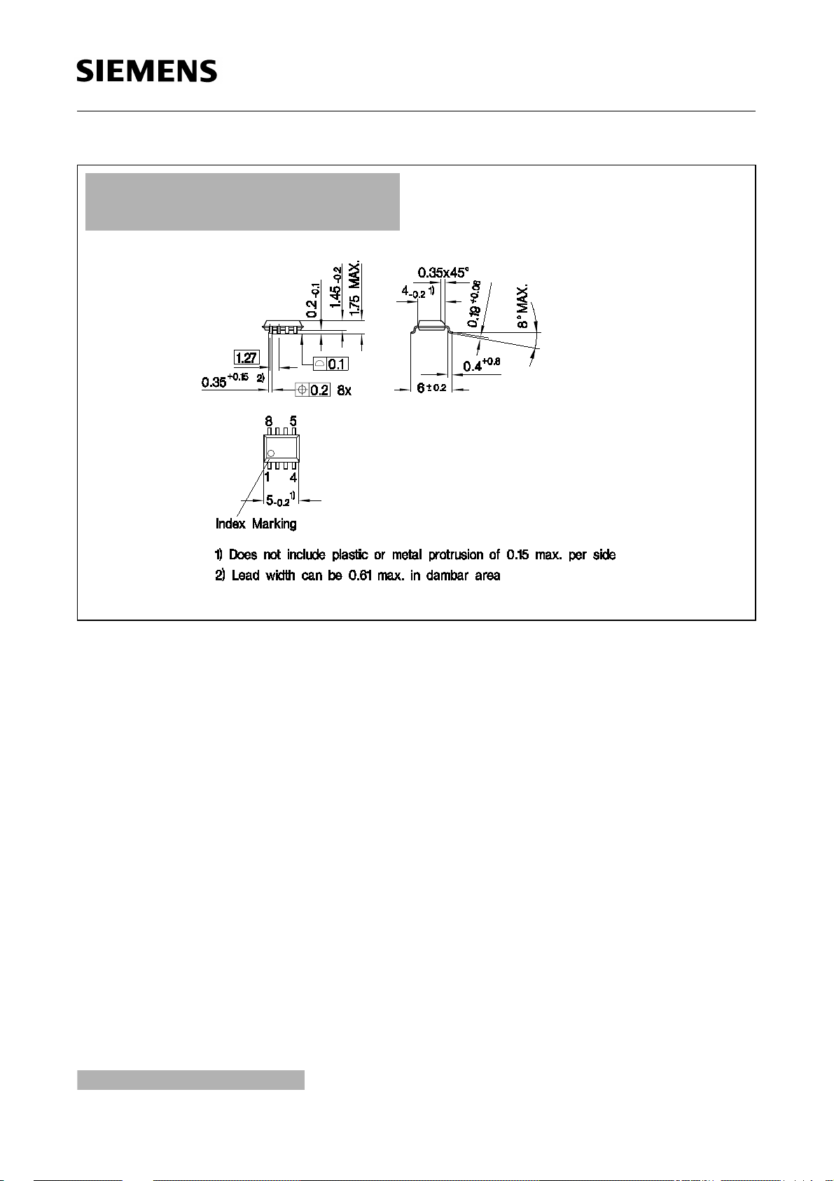
Plastic Package, P-DSO-8-1
(Plastic Dual Small Outline Package)
TDA 4862
GPS05121
Sorts of Packing
Package outlines for tubes, trays etc. are contained in our
Data Book “Package Information”.
SMD = Surface Mounted Device
Semiconductor Group 17 1998-02-16
Dimensions in mm
 Loading...