

Page 1

INTEGRATED CIRCUITS
DATA SH EET
TDA4821P
Autosize IC for colour monitors
Product specification
File under Integrated Circuits, IC02
2000 Feb 09
Page 2

Philips Semiconductors Product specification
Autosize IC for colour monitors TDA4821P
FEATURES
• Measuring of six horizontal and four vertical timing
parameters as follows:
– Horizontal:syncwidth,sync period, video start, video
end and horizontal flyback pulse start and end
– Vertical: sync width, sync period, first line of video
active and last line of video active.
• Detection of H-sync and V-sync polarity
• I2C-bus interface (maximum clock frequency 400 kHz)
for read-out of data and write data of the internal clock
multiplier using double byte (16-bit format)
• Flexible digital clock input with built-in and (via I2C-bus)
adjustable clock multiplier; internal clock is 48 MHz
(typical value)
• Horizontal measurements are expressed in number of
clock pulses; precision is approximately 20 ns at
48 MHz and can be improved if external averaging
methods are used
• Vertical measurements are expressed in number of
lines
• Internal buffer keep I2C-bus registers stable between
the V-sync pulses, allowing for asynchronous read-out.
The advantages are:
• A more user friendlyadjustment forany undefinedvideo
mode by simply pressing a button
• Factory alignment for a reduced number of modes
• Saving of EEPROM storage space for factory and user
modes.
The activation of the autosizing function can be done on
user command or automatically on any mode change.
Whenautosizing isactivated whilethescreen isonly partly
active or consists of sub-windows, the picture size will
increase, butnot more than therange limits of themonitor
allow.
GENERAL DESCRIPTION
The TDA4821P performs the ‘autosize’ feature for colour
monitors. The IC measures the timing of active H/V video
withrespect tothe H-syncand V-syncpulsesand alsowith
respect tothe horizontal flybackpulse in orderto allow the
microcontrollerto adjustthe displaysettingsautomatically,
in particularparameters HSIZE, VSIZE,HPOS andVPOS.
ORDERING INFORMATION
TYPE
NUMBER
TDA4821P DIP20 plastic dual in-line package; 20 leads (300 mil) SOT146-1
NAME DESCRIPTION VERSION
PACKAGE
2000 Feb 09 2
Page 3

Philips Semiconductors Product specification
Autosize IC for colour monitors TDA4821P
QUICK REFERENCE DATA
Voltages measured with respect to pins V
SYMBOL PARAMETER CONDITIONS MIN. TYP. MAX. UNIT
V
DD(core)
V
DD(I/O)
V
DD(PLL)
V
VIN1
core supply voltage (pin 15) 3 3.3 3.6 V
I/O supply voltage (pin 6) 3 3.3 3.6 V
PLL supply voltage (pin 3) 3 3.3 3.6 V
video channel 1 input voltage
(pin 1)
V
VIN2
video channel 2 input voltage
(pin 2)
V
VIN3
video channel 3 input voltage
(pin 19)
V
clamp(ref)
default clamping level for video
channel inputs (pins 1, 2 and 19)
V
slice
slicing voltage for video
comparators
f
clk(ext)
external input clock frequency
(pin 4)
f
clk(int)
M
clk
t
res(h)
internal clock frequency f
clock multiplying factor adjustable via I2C-bus 1 − 8 −
time resolution for horizontal
measurements
f
SCL
I2C-bus serial clock frequency −−400 kHz
SS(I/O)
and V
SS(core)
.
AC-coupled with 10 nF 0 − VDD− 0.5 V
AC-coupled with 10 nF 0 − VDD− 0.5 V
AC-coupled with 10 nF 0 − VDD− 0.5 V
internal default value 360 400 440 mV
450 500 550 mV
4 − 16 MHz
clk(int)=fclk(ext)
without external
× M
clk
18 48 72 MHz
− 20 − ns
averaging methods;
f
= 48 MHz
clk(int)
2000 Feb 09 3
Page 4

Philips Semiconductors Product specification
Autosize IC for colour monitors TDA4821P
BLOCK DIAGRAM
handbook, full pagewidth
R, G, B
video
inputs
horizontal
vertical
+3.3 V
+3.3 V
sync
pulse
sync
pulse
V
DD(PLL)
V
SS(I/O)
V
DD(I/O)
VIN1
VIN2
CLK
HS
VS
1
20
LEV
VIDEO COMPARATORS
2
3
4
5
6
7
8
CLOCK PLL
DIGITAL CORE
HORIZONTAL
POLARITY
DETECTION
VERTICAL
POLARITY
DETECTION
VERTICAL
MEASUREMENT
TDA4821P
TEST MODES
HORIZONTAL
MEASUREMENT
19
18
17
16
15
14
VIN3
T1
CLP
V
SS(core)
V
DD(core)
T2
+3.3 V
video
clamping
pulse
+3.3 V
horizontal
flyback
pulse
POR
HFB
9
10
POWER-ON
RESET
Syncpol
Fig.1 Block diagram.
2000 Feb 09 4
VlstVid
VfstVid
Vperiod
VsWidth
I2C-BUS REGISTERS
Rddat
Subaddr
I2C-BUS
INTERFACE
HsWidth
Wren
Hperiod
Wrdat
HlstVid
HfstVid
Hfbstrt
Hfbstop
MHB651
13
SDA
12
SCL
11
TC
Page 5
Philips Semiconductors Product specification
Autosize IC for colour monitors TDA4821P
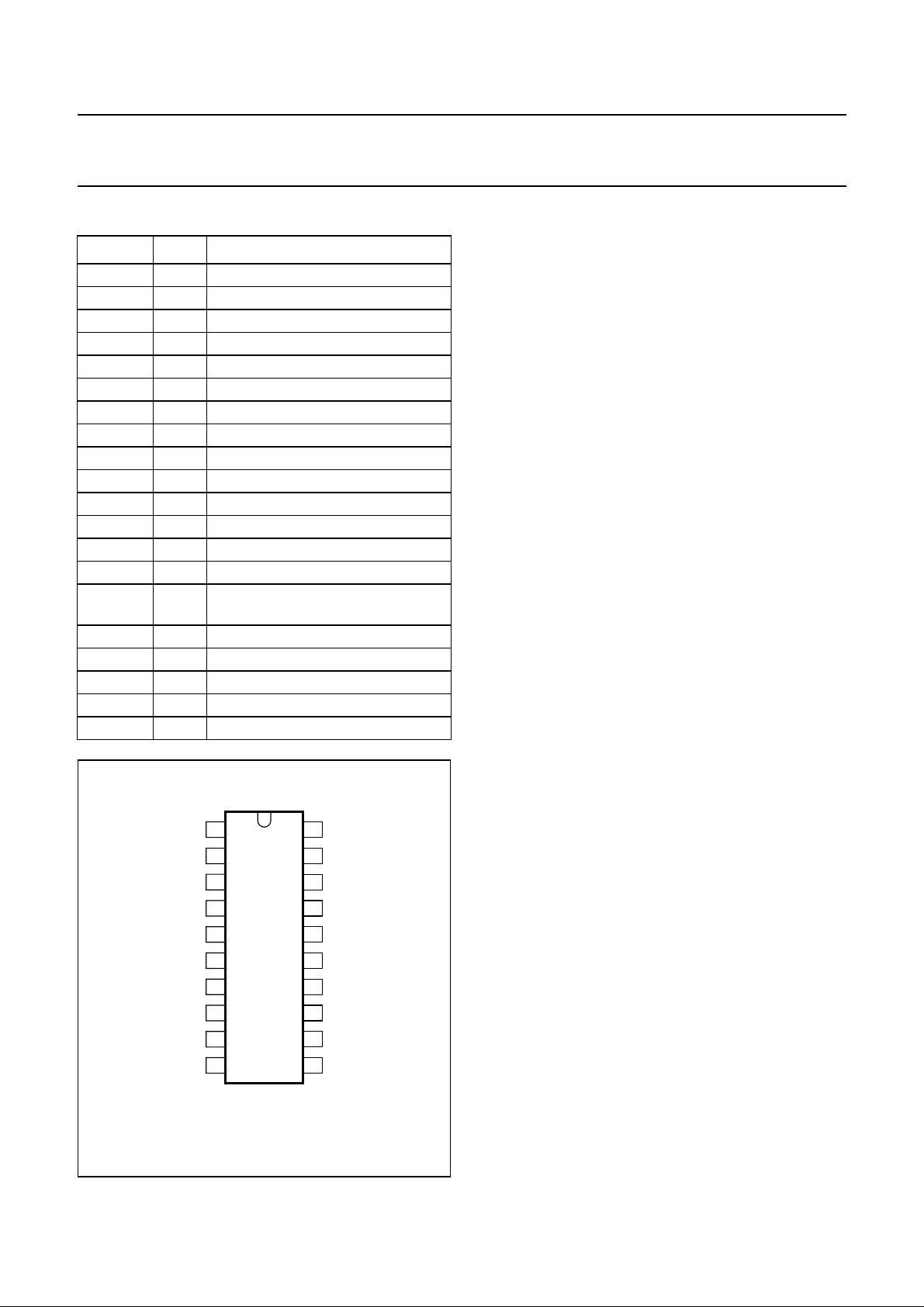
PINNING FUNCTIONAL DESCRIPTION
SYMBOL PIN DESCRIPTION
VIN1 1 video channel 1 input
VIN2 2 video channel 2 input
V
DD(PLL)
3 analog supply voltage of PLL
CLK 4 clock input
V
SS(I/O)
V
DD(I/O)
5 ground of input/output circuit
6 supply voltage of input/output circuit
HS 7 horizontal sync pulse input
VS 8 vertical sync pulse input
POR 9 Power-on reset input
HFB 10 horizontal flyback pulse input
TC 11 test control input
SCL 12 I
SDA 13 I
2
C-bus serial clock input
2
C-bus serial data input/output
T2 14 test mode 2 input
V
DD(core)
15 supply voltage of digital core and
comparator
V
SS(core)
16 ground of digital core
CLP 17 video clamping pulse input
T1 18 test mode 1 input
VIN3 19 video channel 3 input
LEV 20 video clamping level input
The TDA4821P consists of an RGB video comparator
input stage (see Fig.1), a clock PLL for multiplying the
external clock and a digital core which includes the
comparators forH-sync, V-sync and H-flybackpulses, the
polarity detection, the horizontal and vertical time
measurement blocks, the I2C-bus registers and interface
and the Power-on reset circuitry.
RGB video input stage
Three video input comparators are provided, suitable for
AC-coupling with capacitors of approximately 10 nF on
each input. The input pins VIN1, VIN2 and VIN3 are
suitable forthe RGBvideo signals. Thethree input signals
are internally applied to an OR-circuit, so the presence of
one video signal is sufficient to activate the capture
registers.
A positive pulse is needed on pin CLP for black level
clamping. This clamping pulse must not coincide with a
possible Sync-On-Green (SOG) because SOG will not be
detected by this IC.
The black level of the video signal on pins VIN1, VIN2
and VIN3 is clamped internally to 400 mV (typical value).
This clamping level is determined by an internal divider
which is available on pin LEV and can be adjusted by an
additional external resistor divider connected to pin LEV
(see Fig.5).A small HF decoupling capacitor isneeded on
pin LEV.
handbook, halfpage
V
VIN1
VIN2
DD(PLL)
CLK
V
SS(I/O)
V
DD(I/O)
POR
HFB
HS
VS
1
2
3
4
5
TDA4821P
6
7
8
9
10
MHB652
20
19
18
17
16
15
14
13
12
11
LEV
VIN3
T1
CLP
V
SS(core)
V
DD(core)
T2
SDA
SCL
TC
Fig.2 Pin configuration.
2000 Feb 09 5
The video slicing level for the detection of active video is
500 mV(typical value).This level isapproximately 100 mV
above the blacklevel and is fixed byan additional internal
resistor divider fromthe 3.3 V supply voltage; it cannot be
modified. All signals which exceed this level are
recognized as active video. The difference between the
video slicing level andthe clamping level is adjustable via
pin LEV.
Example: changing the voltage on pin LEV from
400 to 200 mV increases the threshold voltage for the
detection of active video from 100 to 300 mV.
Page 6

Philips Semiconductors Product specification
Autosize IC for colour monitors TDA4821P
Clock PLL
In order to measure the horizontal timing with sufficient
precision, it is recommended to set the frequency of the
internalreference clockto 48 MHz.Thisclock isgenerated
by amultiplying PLL fromthe external clocksignal applied
to pin CLK. The ratio between the internal and external
clock frequency (clock multiply factor is M
clk
) is
programmable from 1 to 8 (viathe I2C-bus). For instance,
for an externalclock frequency of 8 MHz, a multiply factor
M
= 6is neededto achieveaninternal referenceclock of
clk
48 MHz.
After power-on of the IC and with an inactive I2C-bus, the
default value of factor M
is set to 2.
clk
Sync and flyback pulse comparators and polarity
detection
The horizontal and vertical sync pulse input circuits on
pins HS and VS are able to handle both 5 or 3.3 V level
H/V sync pulses. The H-sync and V-sync signals are
internally preprocessed by edge detectors which deliver
positive pulses at the rising and falling edges of the input
signals and are followed by auto-polarity correction
stages. The polarity status of both sync signals will be
detected and corrected and is available as the I2C-bus
status bits Hpol and Vpol. A positive polarity means that
the duty cycle is smaller than 50% (bit Hpol = 0 or
bit Vpol = 0) and for a negative polarity the duty cycle is
larger than 50%.
The horizontal flyback pulse on pin HFB is internally
preprocessed by an edgedetector in the same way asfor
H-sync and V-sync pulses. The measurement of the
position of the horizontal flyback pulse provides further
information for the monitor microcontroller for a correct
auto-adjustment of the picture within the scanned raster
area.
Horizontal and vertical timing measurements
For eachvertical period the IC performs sixhorizontal and
four vertical measurements (see Figs 3 and 4).
The leadingedge of the nextvertical sync pulseis used to
transfer the previous measurement results to the I2C-bus
data read registers and to reset the internal counters for
the next full timing measurement cycle. In this way the
I2C-bus data registers will always contain stable
sample-and-hold data(assuming that thesync signalsare
stable) and they can be read-out via the I2C-bus by an
external microcontroller for automatic adaption of the
display geometry.
Moreover, measuring the width of the sync pulses gives
more advantages such as:
• A better mode discrimination
• In some cases the horizontal PLL of the deflection
controllers operates on the leading edge of the sync
pulse, in other cases in the middle of the sync pulse.
VERTICAL TIMING MEASUREMENTS
The parameters are measuredwith respect to the leading
edgeof theV-sync pulse(see Fig.3).At eachleading edge
of the V-sync pulse on pin VS a 12-bit counter is started.
The four vertical timings (see Table 1) are counted as a
number of H-sync pulses on pin HS and stored in buffer
registers.The contentsof thesebuffer registersare copied
to the I2C-bus registers on every next V-sync pulse with
the additionof LSBs (logic 0) forcompleting the full2-byte
data (see Table 4).
The maximum line count is 4095. With Enhanced
Graphics Adapter (EGA) systems with approximately
400 lines at 31.45 kHz, the lower line count will be 9 bits
long only but the resolution is still better than 0.25%. No
provisions are included for recognizing interlaced sync
signals with or without equal vertical periods.
2000 Feb 09 6
Page 7

Philips Semiconductors Product specification
Autosize IC for colour monitors TDA4821P
Table 1 Vertical timing measurements
TIMING BITS CONDITIONS
VsWidth 8 trailing edge of pulse on pin VS
VfstVid 12 first line with active video on pins VIN1, VIN2 or VIN3
VlstVid 12 last line with active video on pins VIN1, VIN2 or VIN3
Vperiod 12 next leading edge of pulse on pin VS
handbook, full pagewidth
vertical sync
(pin VS)
VsWidth
R, G, B video inputs
(pins VIN1, VIN2, VIN3)
VfstVid
horizontal sync
Fig.3 Vertical timing.
HORIZONTAL TIMING MEASUREMENTS
The parameters are measuredwith respect to the leading
edge ofthe H-syncpulses (see Fig.4).At the leadingedge
of the H-sync pulse on pin HS a 12-bit clock counter is
started (nominal internal clock frequency is 48 MHz).
The six horizontal timings (see Table 2) are countered as
a number of internal clock pulses and stored in buffer
registers.The contentsof thesebuffer registersare copied
to theI2C-bus dataregisters onevery nextleading edgeof
the V-sync pulse with the addition of LSBs (logic 0) for
completing the full 2-byte data.
Vperiod
VlstVid
MHB653
The measurements of HsWidth, Hperiod, Hfbstrt and
Hfbstop in line 64 preventwrong datacapturing causedby
post-equalizing sync pulses.
The minimum horizontalfrequency is 12 kHz and Hperiod
displays the full 12 bits. At 125 kHz, the shorter Hperiod
will display 9 bits only but the resolution is still better
than 0.25%.
2000 Feb 09 7
Page 8

Philips Semiconductors Product specification
Autosize IC for colour monitors TDA4821P
Table 2 Horizontal timing measurements
TIMING BITS CONDITIONS REMARKS
HsWidth 8 trailing edge of pulse on pin HS in line 64 only
Hperiod 12 next leading edge of pulse on pin HS in line 64 only
Hfbstrt 12 leading edge of pulse on pin HFB in line 64 only
Hfbstop 12 trailing edge of pulse on pin HFB in line 64 only
HfstVid 12 first active video on pins VIN1, VIN2 or VIN3 in any line since last leading edge of pulse on
pin VS
HlstVid 12 last active video on pins VIN1, VIN2 or VIN3 in any line since last leading edge of pulse on
pin VS
handbook, full pagewidth
horizontal sync
flyback pulse
R, G, B video inputs
(pins VIN1, VIN2, VIN3)
reference clock
(pin HS)
horizontal
(pin HFB)
HsWidth
Hperiod
threshold level
Hfbstop
Hfbstrt
HfstVid
HlstVid
MHB654
Fig.4 Horizontal timing.
2000 Feb 09 8
Page 9

Philips Semiconductors Product specification
Autosize IC for colour monitors TDA4821P
EXAMPLE OF A MEASUREMENT
On a 17-inch-screen the picture width is 320 mm. At a
horizontal frequency of 70 kHz the active video is 11 µs.
Thus, with a measuring clock of 48 MHz, there are
528 clock pulses. The start and end of the video with
respect to the leading edge of the H-sync pulse can both
be measured with an accuracy of one clock pulse. On
screen one clock pulse corresponds to mm.
An external microcontroller takes the measurements and
aftercalculation thenew settingswillbe downloadedto the
deflection controller e.g. TDA4854, which has register
steps corresponding to 0.4 mm on the screen. For this
example, the positioning accuracy of the total auto-image
concept will be in the range of: 0.6 + 0.4 = 1 mm.
Since theclock isasynchronous, repeatedmeasurements
may show jumping between two values. If the external
microcontroller takesthe averageof afew measurements,
the final accuracy will be improved and, as a result, the
total accuracy (measurement accuracy and register step
size) will be improved too.
OTHER SYNC PULSE CONDITIONS
The IC needs both the H-sync and V-sync pulses on
pins HS and VS respectively, for correct operation of the
capture registers.
The initial contents of the I2C-bus registers are random.
At least two V-sync pulses (one full vertical period)
together withthe normalH-sync pulsesare needed before
the contents become valid. Without H-sync pulses (but
with V-sync pulses) the register contents will be random.
Without V-sync pulses (but with H-sync pulses) the
register contents will be random too and the same will
happen if both H-sync and V-sync pulses are missing,
again the register contents will be random.
320
--------- 528
0.6=
Table 3 Register values for missing RGB video or
horizontal flyback signals
CONDITIONS REGISTER VALUE
No R, G or B
video signal
No horizontal
flyback signal
2
C-bus interface and registers
I
The I2C-bus device address is 0111 010X, which means
74H for write and 75H for read.
The I2C-bus interface can handle standard I2C-bus
features, including auto-increment in the read mode, so
data byte bydata byte can be read without sending a new
subaddress each time. The interface can handle both
100 and 400 kHz I2C-bus standards. Pins SDA and SCL
(5 V tolerable I/O) have digital filters, which remove all
spikes smallerthan 60 nsand the thresholdlevels on both
pins are TTL compatible.
The contentsof timing measurements, syncpulse polarity
and the clock multiplication factor are stored in
22 registersof 8-bitlength (see Table 4).All readregisters
are double buffered and written simultaneously on the
leadingedge oftheV-sync pulse.Thatmeans thatthe data
is stable for one complete field.
VfstVid maximum:
MSB = FF and LSB = F0
VlstVid zero:
MSB = 0 and LSB = 0
HfstVid maximum:
MSB = FF and LSB = F0
HlstVid zero:
MSB = 0 and LSB = 0
Hfbstrt maximum:
MSB = FF and LSB = F0
Hfbstop maximum:
MSB = FF and LSB = F0
In the event of the application of a composite sync signal
to pin HS, the contents of the vertical capture registers
may differslightly fromthe actualline count, dependingon
the number of missing or additional H-sync pulses and/or
equalizing pulses during the vertical blanking time.
MISSING RGB VIDEO OR HORIZONTAL FLYBACK SIGNALS
Ifthe RGBvideosignals orthehorizontal flybacksignal are
belowthe thresholdlevel thesesignals cannotbe detected
(missing signals). In that event the video and flyback
registers will have the default values (see Table 3).
2000 Feb 09 9
Page 10

Philips Semiconductors Product specification
Autosize IC for colour monitors TDA4821P
Table 4 I2C-bus registers and their contents
SUBADDRESS REGISTER
HEX NAME FUNCTION D7 D6 D5 D4 D3 D2 D1 D0
00 VsWidth (MSB) V-sync width R b15 b14 b13 b12 b11 b10 b9 b8
01 VsWidth (LSB) V-sync width R 0 0000000
02 VfstVid (MSB) start video after V-sync R b15 b14 b13 b12 b11 b10 b9 b8
03 VfstVid (LSB) start video after V-sync R b7 b6 b5 b4 0000
04 VlstVid (MSB) stop video after V-sync R b15 b14 b13 b12 b11 b10 b9 b8
05 VlstVid (LSB) stop video after V-sync R b7 b6 b5 b4 0000
06 Vperiod (MSB) V-sync cycle time R b15 b14 b13 b12 b11 b10 b9 b8
07 Vperiod (LSB) V-sync cycle time R b7 b6 b5 b4 0000
08 HsWidth (MSB) H-sync width R b15 b14 b13 b12 b11 b10 b9 b8
09 HsWidth (LSB) H-sync width R 0 0000000
0A HfstVid (MSB) start video after H-sync R b15 b14 b13 b12 b11 b10 b9 b8
0B HfstVid (LSB) start video after H-sync R b7 b6 b5 b4 0000
0C HlstVid (MSB) stop video after H-sync R b15 b14 b13 b12 b11 b10 b9 b8
0D HlstVid (LSB) stop video after V-sync R b7 b6 b5 b4 0000
0E Hperiod (MSB) H-sync cycle time R b15 b14 b13 b12 b11 b10 b9 b8
0F Hperiod (LSB) H-sync cycle time R b7 b6 b5 b4 0000
10 Hfbstrt (MSB) start flyback after H-sync R b15 b14 b13 b12 b11 b10 b9 b8
11 Hfbstrt (LSB) start flyback after H-sync R b7 b6 b5 b4 0000
12 Hfbstop (MSB) stop flyback after H-sync R b15 b14 b13 b12 b11 b10 b9 b8
13 Hfbstop (LSB) stop flyback after H-sync R b7 b6 b5 b4 0000
14 Sync polarities sync polarities R 0 00000Hpol Vpol
20 Mclk clock multiplier W 0 0000b2b1b0
MSB LSB
R/W
Table 5 Description of the clock multiplier
REGISTER Mclk
b2 b1 b0
001 1
0 1 0 2 (default after power-on)
011 3
100 4
101 5
110 6
111 7
000 8
2000 Feb 09 10
CLOCK MULTIPLICATION FACTOR
Page 11

Philips Semiconductors Product specification
Autosize IC for colour monitors TDA4821P
LIMITING VALUES
In accordance with the Absolute Maximum Rating System (IEC 60134).
SYMBOL PARAMETER CONDITIONS MIN. MAX. UNIT
V
DD(core)
V
DD(I/O)
V
DD(PLL)
V
i(n)
I
DD(core)
I
DD(I/O)
I
DD(PLL)
I
o(SDA)
P
tot
T
stg
T
amb
T
j
V
es
core supply voltage −0.5 +4 V
I/O supply voltage −0.5 +4 V
PLL supply voltage −0.5 +4 V
input voltage:
on pins HS, VS, SCL and SDA −0.5 +5.5 V
on all other I/O pins −0.5 VDD+ 0.5 V
core supply current − 30 mA
I/O supply current external load on
− 30 mA
pin SDA
PLL supply current − 1mA
output current on pin SDA external load − 20 mA
total power dissipation − 200 mW
storage temperature −40 +125 °C
ambient temperature −20 +70 °C
junction temperature −20 +125 °C
electrostatic handling voltage note 1 −250 +250 V
note 2 −4000 +4000 V
Notes
1. Machine model: equivalent to discharging a 200 pF capacitor through a 0 Ω series resistor (‘0 Ω’ is actually
0.75 µH+10Ω).
2. Human body model: equivalent to discharging a 100 pF capacitor through a 1500 Ω series resistor.
THERMAL CHARACTERISTICS
SYMBOL PARAMETER CONDITIONS VALUE UNIT
R
th(j-a)
thermal resistance from junction to ambient in free air 80 K/W
2000 Feb 09 11
Page 12

Philips Semiconductors Product specification
Autosize IC for colour monitors TDA4821P
CHARACTERISTICS
VDD= 3.3 V; T
SYMBOL PARAMETER CONDITIONS MIN. TYP. MAX. UNIT
Supplies
V
DD(core)
V
DD(I/O)
V
DD(PLL)
I
DD(core)
I
DD(I/O)
I
DD(PLL)
P
tot
RGB input stage
V
VIN1
V
VIN2
V
VIN3
V
CLP
V
clamp(ref)
V
clamp(video)
V
slice
t
d(video)
I
clamp
I
LI(video)
V
clamp
V
clamp(adj)
C
LEV(min)
V
th(H)
V
th(L)
t
W(clamp)
=25°C; voltages measured with respect to ground (pins VSS); unless otherwise specified.
amb
core supply voltage (pin 15) 3 3.3 3.6 V
I/O supply voltage (pin 6) 3 3.3 3.6 V
PLL supply voltage (pin 3) 3 3.3 3.6 V
core supply current (pin 15) f
I/O supply current (pin 6) no load on digital output
= 48 MHz − 10 14 mA
clk(int)
f
= 24 MHz − 68mA
clk(int)
−−300 µA
pins
PLL supply current (pin 3) − 400 800 µA
total power dissipation −−100 mW
video channel 1 input voltage
AC-coupled with 10 nF 0 − VDD− 0.5 V
(pin 1)
video channel 2 input voltage
AC-coupled with 10 nF 0 − VDD− 0.5 V
(pin 2)
video channel 3 input voltage
AC-coupled with 10 nF 0 − VDD− 0.5 V
(pin 19)
clamping active input voltage
0 − V
DD
V
(pin 17)
default clamping level for video
internal default value 360 400 440 mV
channel inputs
(pins 1, 2 and 19)
clamping voltage range for
video channel inputs
externally adjustable
range
100 400 440 mV
(pins 1, 2 and 19)
slicing voltage for video
450 500 550 mV
comparators
video comparator delay time V
clamping current V
VIN=Vslice
clamp
+30mV − 10 25 ns
= 400 mV;
−−10 mA
clamp = HIGH
video input leakage current clamp = LOW −−1µA
clamping level voltage (pin 20) internal default value 380 400 420 mV
adjustable clamping level
voltage range (pin 20)
minimum capacitance at LEV
externally adjustable
range
0 − 420 mV
110−nF
(pin 20)
clamping active threshold
voltage (pin 17)
clamping inactive threshold
voltage (pin 17)
clamping pulse width (pin 17) video inputsAC-coupled
rising edge (hysteresis
input)
falling edge (hysteresis
input)
1.3 − 1.9 V
0.9 − 1.35 V
300 −−ns
with 10 nF
2000 Feb 09 12
Page 13

Philips Semiconductors Product specification
Autosize IC for colour monitors TDA4821P
SYMBOL PARAMETER CONDITIONS MIN. TYP. MAX. UNIT
Clock PLL
f
clk(ext)
external input clock frequency
(pin 4)
f
clk(int)
M
clk
t
res(h)
internal clock frequency f
clock multiplication factor adjustable via I2C-bus 1 − 8 −
time resolution for horizontal
measurements
V
i(CLK)
input voltage on pin CLK (pin 4) 0 − V
Digital inputs and outputs
clk(int)=fclk(ext)
× M
default value after
power-on; I
2
C-bus not
active
without external
averaging methods:
f
= 48 MHz − 20 − ns
clk(int)
f
= 72 MHz − 14 − ns
clk(int)
clk
4 − 24 MHz
18 48 72 MHz
− 2 −−
DD
V
INPUT PINS HS, VS, POR AND HFB (PINS 7, 8, 9 AND 10)
V
IL
V
IH
I
LI
V
i(9,10)
V
i(7,8)
t
W
LOW-level input voltage −−0.8 V
HIGH-level input voltage 2 −−V
input leakage current −−1µA
input voltage on pins 9 and 10 0 − V
input voltage on pins 7 and 8 0 − 5.25 V
pulse width of input signals on
f
= 48 MHz 100 −−ns
clk(int)
pins 7, 8 and 10
I2C-BUS INPUT/OUTPUT PINS SCL AND SDA (PINS 12 AND 13)
V
IL
V
IH
I
LI
V
OL
V
OH
V
i(12,13)
LOW-level input voltage −−0.8 V
HIGH-level input voltage 2 −−V
input leakage current −−1µA
LOW-level output voltage I
HIGH-level output voltage I
=3mA −−0.4 V
o(13)
= −3 mA 2.4 −−V
o(13)
input voltage on pins 12 and 13 external pull-up resistor
to 5 V supply
I
o(13)
f
SCL
output current on pin 13 external load −−3mA
I2C-bus serial clock frequency −−400 kHz
DD
0 − 5.25 V
V
2000 Feb 09 13
Page 14

Philips Semiconductors Product specification
Autosize IC for colour monitors TDA4821P
APPLICATION INFORMATION
handbook, full pagewidth
R, G, B
video
inputs
+3.3 V
external
clock
input
optional if
5 V supply is
available only
+5 V
100 Ω
+3.3 V
H-sync
V-sync
necessary only if
H-sync coincides
with V-sync
50 Ω
50 Ω
50 Ω
10 µF
10 Ω
27 Ω
27 Ω
27 Ω
+3.3 V
200 Ω
200 Ω
50 Ω
10 nF
10 nF
10 nF
V
DD(PLL)
47 nF
V
SS(I/O)
V
DD(I/O)
150
pF
VIN1
VIN2
CLK
optional for
V
clamp(video)
1
20
VIDEO COMPARATORS
2
3
4
5
6
7
HS
8
VS
CLOCK PLL
DIGITAL CORE
HORIZONTAL
POLARITY
DETECTION
VERTICAL
POLARITY
DETECTION
MEASUREMENT
VERTICAL
TDA4821P
TEST MODES
HORIZONTAL
MEASUREMENT
LEV
19
VIN3
18
T1
CLP
V
SS(core)
V
DD(core)
T2
3.3 kΩ
2.4 kΩ
17
16
15
14
10 nF
47 nF
+3.3 V
clamping
+3.3 V
≠ 400 mV
video
pulse
horizontal
flyback
pulse
C
+3.3 V
(1)
h
270 nF
390 kΩ
+3.3 V
R
h
200 Ω
1 kΩ
POR
HFB
9
POWER-ON
RESET
10
Syncpol
(1) Ch and Rh are application dependent.
Fig.5 Application diagram.
2000 Feb 09 14
VlstVid
VfstVid
Vperiod
VsWidth
I2C-BUS REGISTERS
Rddat
Subaddr
I2C-BUS
INTERFACE
HsWidth
Wren
Hperiod
Wrdat
HlstVid
Hfbstrt
HfstVid
Hfbstop
13
12
11
MHB655
SDA
SCL
TC
100 Ω
100 Ω
I2C-bus
interface
Page 15

Philips Semiconductors Product specification
Autosize IC for colour monitors TDA4821P
PACKAGE OUTLINE
DIP20: plastic dual in-line package; 20 leads (300 mil)
SOT146-1
seating plane
L
Z
20
pin 1 index
1
D
A
2
A
A
1
e
b
11
w M
b
1
E
10
M
E
c
(e )
1
M
H
0 5 10 mm
scale
DIMENSIONS (inch dimensions are derived from the original mm dimensions)
A
UNIT
mm
inches
Note
1. Plastic or metal protrusions of 0.25 mm maximum per side are not included.
max.
OUTLINE
VERSION
SOT146-1
A
min.
A
1 2
max.
IEC JEDEC EIAJ
b
1.73
1.30
0.068
0.051
b
0.53
0.38
0.021
0.015
1
cD E e M
0.36
0.23
0.014
0.009
REFERENCES
(1) (1)
26.92
26.54
1.060
1.045
SC-603MS-001
2000 Feb 09 15
6.40
6.22
0.25
0.24
M
e
L
1
3.60
8.25
3.05
7.80
0.14
0.32
0.12
0.31
EUROPEAN
PROJECTION
H
E
10.0
0.2542.54 7.62
8.3
0.39
0.010.10 0.30
0.33
ISSUE DATE
w
95-05-24
99-12-27
Z
max.
2.04.2 0.51 3.2
0.0780.17 0.020 0.13
(1)
Page 16

Philips Semiconductors Product specification
Autosize IC for colour monitors TDA4821P
SOLDERING
Introduction to soldering through-hole mount
packages
This text gives a brief insight to wave, dip and manual
soldering.A morein-depth accountofsoldering ICscan be
found in our
Packages”
Wave soldering is the preferred method for mounting of
through-hole mount IC packages on a printed-circuit
board.
Soldering by dipping or by solder wave
The maximum permissible temperature of the solder is
260 °C; solder at this temperature must not be in contact
with the joints for more than 5 seconds.
Suitability of through-hole mount IC packages for dipping and wave soldering methods
DBS, DIP, HDIP, SDIP, SIL suitable suitable
Note
1. For SDIP packages, the longitudinal axis must be parallel to the transport direction of the printed-circuit board.
“Data Handbook IC26; Integrated Circuit
(document order number 9398 652 90011).
PACKAGE
Thetotal contacttimeof successivesolder wavesmustnot
exceed 5 seconds.
The device may be mounted up to the seating plane, but
the temperature of the plastic body must not exceed the
specified maximum storage temperature (T
printed-circuit board has been pre-heated, forced cooling
may benecessary immediately after solderingto keep the
temperature within the permissible limit.
Manual soldering
Apply the solderingiron (24 V or less) tothe lead(s) of the
package, either below the seating plane or not more than
2 mm above it. If the temperature of the soldering iron bit
is less than 300 °C it may remain in contact for up to
10 seconds. If the bit temperature is between
300 and 400 °C, contact may be up to 5 seconds.
SOLDERING METHOD
DIPPING WAVE
(1)
stg(max)
). If the
2000 Feb 09 16
Page 17

Philips Semiconductors Product specification
Autosize IC for colour monitors TDA4821P
DEFINITIONS
Data sheet status
Objective specification This data sheet contains target or goal specifications for product development.
Preliminary specification This data sheet contains preliminary data; supplementary data may be published later.
Product specification This data sheet contains final product specifications.
Limiting values
Limiting values given are in accordance with the Absolute Maximum Rating System (IEC 134). Stress above one or
more of the limiting values may cause permanent damage to the device. These are stress ratings only and operation
of the device at these or at any other conditions above those given in the Characteristics sections of the specification
is not implied. Exposure to limiting values for extended periods may affect device reliability.
Application information
Where application information is given, it is advisory and does not form part of the specification.
LIFE SUPPORT APPLICATIONS
These products are not designed for use in life support appliances, devices, or systems where malfunction of these
products can reasonably be expected to result in personal injury. Philips customers using or selling these products for
use in suchapplications do so at theirown risk and agree to fullyindemnify Philips for any damagesresulting from such
improper use or sale.
PURCHASE OF PHILIPS I
2
C COMPONENTS
2
Purchase of Philips I
components inthe I2C systemprovided the system conformsto the I2C specificationdefined by
Philips. This specification can be ordered using the code 9398 393 40011.
C components conveys a license under the Philips’ I2C patent to use the
2000 Feb 09 17
Page 18

Philips Semiconductors Product specification
Autosize IC for colour monitors TDA4821P
NOTES
2000 Feb 09 18
Page 19

Philips Semiconductors Product specification
Autosize IC for colour monitors TDA4821P
NOTES
2000 Feb 09 19
Page 20

Philips Semiconductors – a w orldwide compan y
Argentina: see South America
Australia: 3 Figtree Drive, HOMEBUSH, NSW 2140,
Tel. +61 2 9704 8141, Fax. +61 2 9704 8139
Austria: Computerstr. 6, A-1101 WIEN, P.O. Box 213,
Tel. +43 1 60 101 1248, Fax. +43 1 60 101 1210
Belarus: Hotel Minsk Business Center, Bld. 3, r. 1211, Volodarski Str. 6,
220050 MINSK, Tel. +375 172 20 0733, Fax. +375 172 20 0773
Belgium: see The Netherlands
Brazil: see South America
Bulgaria: Philips Bulgaria Ltd., Energoproject, 15th floor,
51 James Bourchier Blvd., 1407 SOFIA,
Tel. +359 2 68 9211, Fax. +359 2 68 9102
Canada: PHILIPS SEMICONDUCTORS/COMPONENTS,
Tel. +1 800 234 7381, Fax. +1 800 943 0087
China/Hong Kong: 501 Hong Kong Industrial Technology Centre,
72 Tat Chee Avenue, Kowloon Tong, HONG KONG,
Tel. +852 2319 7888, Fax. +852 2319 7700
Colombia: see South America
Czech Republic: see Austria
Denmark: Sydhavnsgade 23, 1780 COPENHAGEN V,
Tel. +45 33 29 3333, Fax. +45 33 29 3905
Finland: Sinikalliontie 3, FIN-02630 ESPOO,
Tel. +358 9 615 800, Fax. +358 9 6158 0920
France: 51 Rue Carnot, BP317, 92156 SURESNES Cedex,
Tel. +33 1 4099 6161, Fax. +33 1 4099 6427
Germany: Hammerbrookstraße 69, D-20097 HAMBURG,
Tel. +49 40 2353 60, Fax. +49 40 2353 6300
Hungary: see Austria
India: Philips INDIA Ltd, Band Box Building, 2nd floor,
254-D, Dr. Annie Besant Road, Worli, MUMBAI 400 025,
Tel. +91 22 493 8541, Fax. +91 22 493 0966
Indonesia: PT Philips Development Corporation, Semiconductors Division,
Gedung Philips, Jl. Buncit Raya Kav.99-100, JAKARTA 12510,
Tel. +62 21 794 0040 ext. 2501, Fax. +62 21 794 0080
Ireland: Newstead, Clonskeagh, DUBLIN 14,
Tel. +353 1 7640 000, Fax. +353 1 7640 200
Israel: RAPAC Electronics, 7 Kehilat Saloniki St, PO Box 18053,
TEL AVIV 61180, Tel. +972 3 645 0444, Fax. +972 3 649 1007
Italy: PHILIPS SEMICONDUCTORS,Via Casati, 23 - 20052 MONZA(MI),
Tel. +39 039 203 6838, Fax +39 039 203 6800
Japan: Philips Bldg 13-37, Kohnan 2-chome, Minato-ku,
TOKYO 108-8507, Tel. +81 3 3740 5130, Fax. +81 3 3740 5057
Korea: Philips House, 260-199 Itaewon-dong, Yongsan-ku, SEOUL,
Tel. +82 2 709 1412, Fax. +82 2 709 1415
Malaysia: No. 76 Jalan Universiti, 46200 PETALING JAYA, SELANGOR,
Tel. +60 3 750 5214, Fax. +60 3 757 4880
Mexico: 5900 Gateway East, Suite 200, EL PASO, TEXAS 79905,
Tel. +9-5 800 234 7381, Fax +9-5 800 943 0087
Middle East: see Italy
Netherlands: Postbus 90050, 5600 PB EINDHOVEN, Bldg. VB,
Tel. +31 40 27 82785, Fax. +31 40 27 88399
New Zealand: 2 Wagener Place, C.P.O. Box 1041, AUCKLAND,
Tel. +64 9 849 4160, Fax. +64 9 849 7811
Norway: Box 1, Manglerud 0612, OSLO,
Tel. +47 22 74 8000, Fax. +47 22 74 8341
Pakistan: see Singapore
Philippines: Philips Semiconductors Philippines Inc.,
106 Valero St. Salcedo Village, P.O. Box 2108 MCC, MAKATI,
Metro MANILA, Tel. +63 2 816 6380, Fax. +63 2 817 3474
Poland: Al.Jerozolimskie 195 B, 02-222 WARSAW,
Tel. +48 22 5710 000, Fax. +48 22 5710 001
Portugal: see Spain
Romania: see Italy
Russia: Philips Russia, Ul. Usatcheva 35A, 119048 MOSCOW,
Tel. +7 095 755 6918, Fax. +7 095 755 6919
Singapore: Lorong 1, Toa Payoh, SINGAPORE 319762,
Tel. +65 350 2538, Fax. +65 251 6500
Slovakia: see Austria
Slovenia: see Italy
South Africa: S.A. PHILIPS Pty Ltd., 195-215 Main Road Martindale,
2092 JOHANNESBURG, P.O. Box 58088 Newville 2114,
Tel. +27 11 471 5401, Fax. +27 11 471 5398
South America: Al. Vicente Pinzon, 173, 6th floor,
04547-130 SÃO PAULO, SP, Brazil,
Tel. +55 11 821 2333, Fax. +55 11 821 2382
Spain: Balmes 22, 08007 BARCELONA,
Tel. +34 93 301 6312, Fax. +34 93 301 4107
Sweden: Kottbygatan 7, Akalla, S-16485 STOCKHOLM,
Tel. +46 8 5985 2000, Fax. +46 8 5985 2745
Switzerland: Allmendstrasse 140, CH-8027 ZÜRICH,
Tel. +41 1 488 2741 Fax. +41 1 488 3263
Taiwan: Philips Semiconductors, 6F, No. 96, Chien Kuo N. Rd., Sec. 1,
TAIPEI, Taiwan Tel. +886 2 2134 2886, Fax. +886 2 2134 2874
Thailand: PHILIPS ELECTRONICS (THAILAND) Ltd.,
209/2 Sanpavuth-Bangna Road Prakanong, BANGKOK 10260,
Tel. +66 2 745 4090, Fax. +66 2 398 0793
Turkey: Yukari Dudullu, Org. San. Blg., 2.Cad. Nr. 28 81260 Umraniye,
ISTANBUL, Tel. +90 216 522 1500, Fax. +90 216 522 1813
Ukraine: PHILIPS UKRAINE, 4 Patrice Lumumba str., Building B, Floor 7,
252042 KIEV, Tel. +380 44 264 2776, Fax. +380 44 268 0461
United Kingdom: Philips Semiconductors Ltd., 276 Bath Road, Hayes,
MIDDLESEX UB3 5BX, Tel. +44 208 730 5000, Fax. +44 208 754 8421
United States: 811 East Arques Avenue, SUNNYVALE, CA 94088-3409,
Tel. +1 800 234 7381, Fax. +1 800 943 0087
Uruguay: see South America
Vietnam: see Singapore
Yugoslavia: PHILIPS, Trg N. Pasica 5/v, 11000 BEOGRAD,
Tel. +381 11 3341 299, Fax.+381 11 3342 553
For all other countries apply to: Philips Semiconductors,
International Marketing & Sales Communications, Building BE-p, P.O. Box 218,
5600 MD EINDHOVEN, The Netherlands, Fax. +31 40 27 24825
© Philips Electronics N.V. SCA
All rights are reserved. Reproduction in whole or in part is prohibited without the prior written consent of the copyright owner.
The information presented in this document doesnot form part of any quotation orcontract, is believed to be accurate andreliable and may be changed
without notice. No liability will be accepted by the publisher for any consequence of its use. Publication thereof does not convey nor imply any license
under patent- or other industrial or intellectual property rights.
2000
Internet: http://www.semiconductors.philips.com
69
Printed in The Netherlands 753504/01/pp20 Date of release: 2000 Feb 09 Document order number: 9397 750 06572
 Loading...