

Page 1
Power Factor Controller
IC for High Power Factor and
Active Harmonic Filter
Features
● IC for sinusoidal line-current consumption
● Power factor approaching 1
● Controls boost converter as an active harmonics filter
● Direct drive of SIPMOS transistor
● Zero crossing detector for discontinuous operation mode
with variable frequency
● 110/220 V AC operation without switchover
● Standby current consumption of 0.5 mA
● Start/stop monitoring circuit for lamp generators
TDA 4814
Bipolar IC
P-DIP-14-1
Type Ordering Code Package
TDA 4814 A Q67000-A8163 P-DIP-14-1
■
■ Not for new design
Semiconductor Group 1 01.96
Page 2
TDA 4814 A
TDA 4814
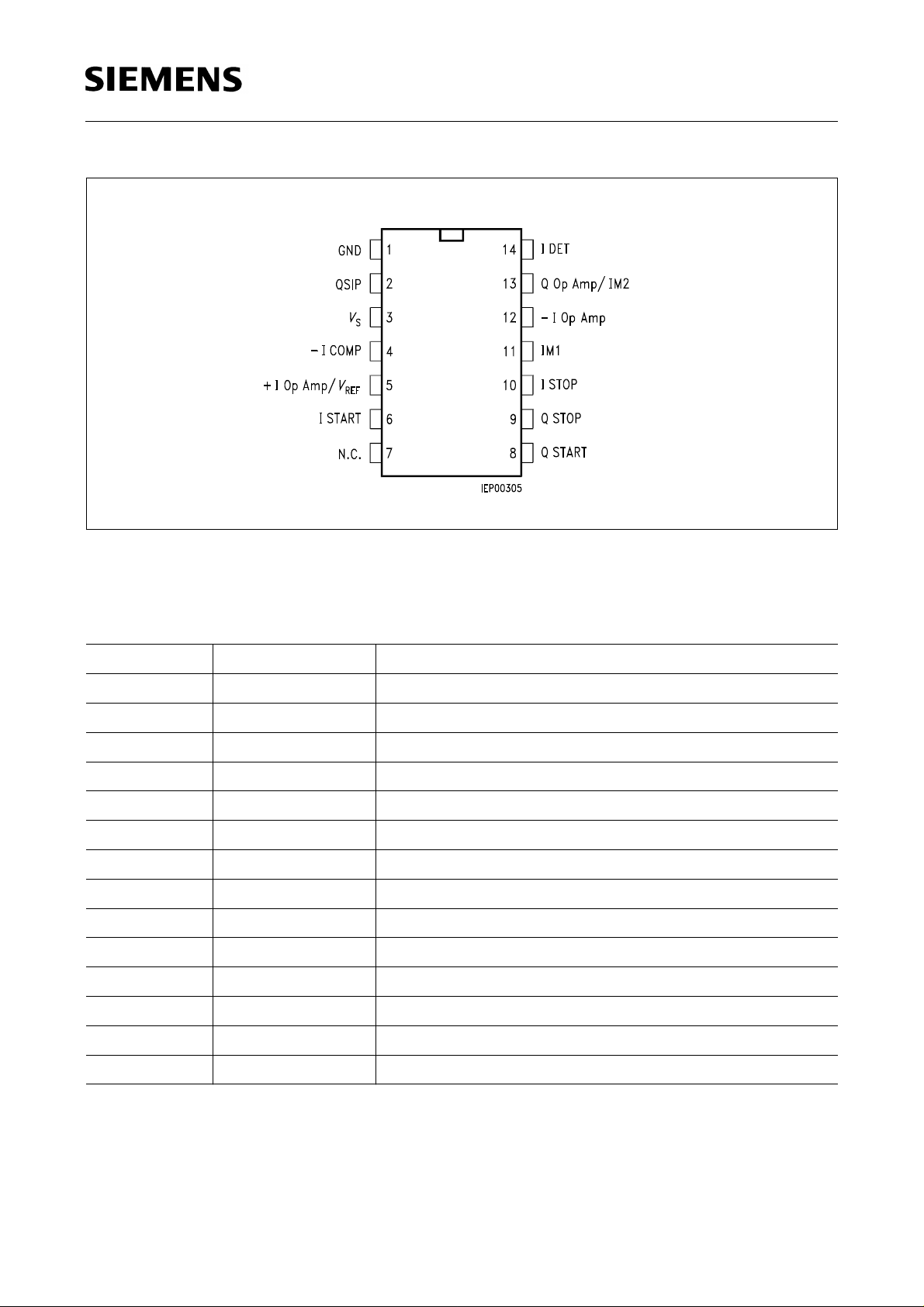
Pin Configurations
(top view)
Pin Definitions and Functions
Pin Symbol Function
1 GND Ground
2 QSIP Driver output
3
V
S
Supply voltage
4–ICOMP Negative comparator input
5+I Op Amp/V
REF
Positive input/reference voltage
6 I START Start input
7 N.C. Not connected
8 Q START Start output
9 Q STOP Stop output
10 I STOP Stop input
11 I M1 Multiplier input M1
12 – I Op Amp Negative input Op amplifier
13 QOp Amp/I M2 Op amplifier output and multiplier input M2
14 I DET Detector input
Semiconductor Group 2
Page 3
TDA 4814
The TDA 4814 A contains all functions for designing electronic ballasts and switched-mode power
supplies with sinusoidal line current consumption and a power factor approaching 1.
They control a boost converter as an active harmonic filter in a discontinuous (triangular shaped
current) mode with variable frequency.
The output voltage of this filter is regulated with high efficiency. Therefore the device can easily be
operated on different line voltages (110/220 VAC) without any switchover.
The on-chip start/stop circuit monitors the lamp generator of electronic ballasts. It starts a selfoscillating lamp generator and shuts it down in the event of malfunction, e.g. if the lamp is defective.
A typical application is in electronic ballasts, especially when a large number of such lamps are
concentrated on one line supply point.
Besides that a separate driver ground (GND QSIP) is implemented.
The TDA 4814 A in a P-DIP-14-1 package.
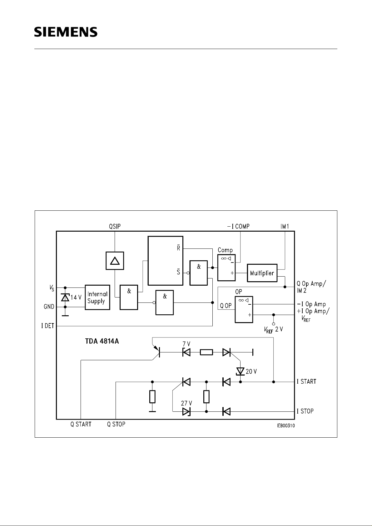
Block Diagram
Semiconductor Group 3
Page 4

TDA 4814
Circuit Description
This device has a conditioning circuit for the internal power supply. It allows standby operation with
very low current consumption (less than 0.5 mA), a hysteresis between enable and switch-off levels
and an internal voltage stabilization. An integrated Z-diode limits the voltage on VS, when
impressed current is fed.
The output driver (Q SIP) is controlled by detector input and current comparator.
The detector input (I DET) which is highly resistive in the operating state reacts on hysteresis-
determined voltage levels. To keep down the amount of circuitry required, clamping diodes are
provided which allow control by a current source.
The operating state of the boost converter choke is sensed via the detector input. H-level means
that the choke discharges and the output driver is inhibited. H-level sets a flip-flop, which stores the
switch-off instruction of the current comparator to reduce susceptibility to interference. As soon as
demagnetization is finished the choke voltage reverses and the detector input is set to L-level, thus
enabling the output driver. This ensures that the choke is always currentless when the SIPMOS
transistor switches on and that no current gaps appear.
The nominal voltage of the multiplier output is compared to the voltage derived from the actual line
current (–I COMP), thus setting the switch-off threshold of the comparator. The current comparator
blocks the output driver when the nominal peak value of the choke current given by the multiplier
output is reached.
This state is maintained in the flip-flop until H-level appears at detector input which takes over the
hold function and resets the flip-flop.
Operating states might occur without any useful detector signal. This is the case with magnetic
saturation of the choke and when the input voltage approaches or exceeds the output voltage as,
for example, during switch-on. The driver remains inhibited for the flip-flop due to the absent set
signal.
The trigger signal can be derived from the subsequent lamp generator, a SMPS control device or,
if neither one of them is available, from the start circuit designed as a pulse generator in the
TDA 4814. The trigger signal level should be so low that with standard operation the signal from the
detector winding dominates.
The multiplier delivers the preset nominal value for the current comparator by multiplying the input
voltage, which determines the nominal waveform (IM1) and the output voltage of the control
amplifier.
The control amplifier stabilizes the output dc voltage of the active harmonic filter in the event of load
and input voltage changes. The control amplifier compares the actual output voltage to a
reference voltage which is provided in the IC and stable with temperature.
Semiconductor Group 4
Page 5

TDA 4814
Output Driver
The output driver is intended to drive a SIPMOS transistor directly. It is designed as a push-pull
stage.
Both the capacitive input impedance and keeping the gate level at zero potential in standby
operation by an internal 10-kΩ-resistor are taken into account. Possible effects on the output driver
by line inductances or capacitive couplings via SIPMOS transistor Miller capacitance are limited by
diodes connected to ground and supply voltage.
Ground Pins
Between the ground pins GND and GND QSIP, a very close and low-impedance connection is to
be established.
Monitoring Circuit (I START, I STOP, Q START, Q STOP)
The monitoring circuit guarantees the secure operation of subsequent circuitries.
Any circuitry that is shut down because of a fault, for instance, cannot be started up again until the
monitoring start (I START / Q START) has turned on and a positive voltage pulse has been
impressed on Q START. This function starts for example the lamp generator of an electronic ballast
or generates auxiliary trigger signals for the detector input.
If there is a defect present (e.g. defective fluorescent lamp) the monitoring stop (I STOP /
Q STOP) will shut down either the entire unit or simply the circuitry that has to be protected. No
restart is possible then until the hold current impressed on I START or Q STOP has been
interrupted (e.g. by a power down).
Semiconductor Group 5
Page 6

Absolute Maximum Ratings
T
= – 40 to 125 ˚C
A
Parameter Symbol Limit Values Unit Notes
min. max.
TDA 4814
Supply voltage
Inputs
Comparator
Op Amp
Multiplier
Outputs
Multiplier
Op Amp
Z current
V
GND I
S
Driver output QSIP V
QSIP clamping diodes I
Input START
STOP
Output START
STOP
V
S
V
ICOMP
V
–I COMP
V
I Op Amp
V
– I Op Amp
V
M1
V
QM
V
Q Op Amp
Z
QSIP
QSIP D
V
I START
V
I STOP
V
Q START
V
Q STOP
/ I
M2
– 0.3 V
– 0.3
– 0.3
– 0.3
– 0.3
– 0.3
– 0.3
– 0.336
Z
33
33
6
6
33
V VZ = Z Voltage
V
V
V
V
V
V
V
0 300 mA Observe P
– 0.3 V
S
V Observe P
– 10 10 mA VQ > VS or
– 0.3
– 0.3
– 10
– 0.3
25
33
3
6
V
V
V
V
–
–
–
–
–
V
> 3 V
S
–
max
max
V
< – 0.3 V
Q
see characteristics
see characteristics
–
–
Detector input
Detector clamping diodes
Capacitance at I START
V
I DET
I
I DET
C
I START
to ground
Junction temperature
Storage temperature
T
j
T
stg
Thermal resistance
system - air
R
th SA
Semiconductor Group 6
0.9
6
V
– 10 10 mA V
– 150 nF –
–
– 55
150
125
˚C
˚C
– 65 K/W –
–
V
–
–
I DET
I DET
> 6 V or
< 0.9 V
Page 7

Absolute Maximum Ratings (cont’d)
T
= – 40 to 125 ˚C
A
Parameter Symbol Limit Values Unit Notes
min. max.
Operating Range
TDA 4814
Supply voltage
V
S
V
S ON
V
Z
V Values for V
S ON
see characteristics
Z-current
Driver current
Operating temperature
I
Z
I
Q QSIP
T
A
0
– 500
200
500
mAmAObserve P
– 25 85 ˚C –
max
–
Characteristics
1)
V
< VS < VZ; TA = – 25 to 85 ˚C
S ON
Parameter Symbol Limit Values Unit
min. typ. max.
Current Consumption
Without load on driver QSIP
and
V
; QSIP LOW
REF
0 V < VS < V
V
< VS > V
S ON
S ON
Z
I
S
I
S
–
2.5
–
5
0.5
6.5
mA
mA
Load on QD with SIPMOS gate;
dynamic operation 50 kHz
V
= 12 V
S
I
S
–
–
15
mA
load on Q = 10 nF
, VZ:
Hysteresis on
Turn-ON threshold for VS rising
Switching hysteresis
V
S
V
SH
V
S hy
Comparator (COMP)
Input offset voltage
Input current
Common-mode input voltage range
V
– I
V
IO
I
IC
Semiconductor Group 7
9.6
1.0
– 10
–
0
10.4–11.2
1.7
–
–
–
10
2
3.5
V
V
mV
µA
V
Page 8

TDA 4814
Characteristics (cont’d)
1)
V
Parameter Symbol Limit Values Unit
Operational Amplifier (Op Amp)
< VS < VZ; TA = – 25 to 85 ˚C
S ON
min. typ. max.
Open-loop voltage gain
Input offset voltage
Input current
Common-mode input voltage range
Output current
Output voltage
Transition frequency
Transition phase
Output Driver (QSIP)
Output voltage high
I
= – 10 mA
Q
Output voltage low
I
= + 10 mA
Q
Output current
rising edge CL = 10 nF
falling edge CL = 10 nF
Reference-Voltage Source
Voltage
0 < I
< 3 mA
REF
Load current
Voltage change
10 V <VS < V
Z
Voltage change
0 mA < I
< 3 mA
REF
Temperature response
G
V0
V
IO
– I
I
V
IC
I
Q Op Amp
V
Q Op Amp
f
T
ϕ
T
V
QH
–
V
QL
–
–
– I
Q
I
Q
V
REF
– I
L
∆V
REF
∆V
REF
∆V
REF
/ ∆T
60
– 30
–
0
– 3
1.2
–
–
5
–
–
–
–
200
250
1.9
0
–
– 0.3
80
–
–
–
–
–
2
120
–
–
–
–
–
300
350
2
–
–
–
–
–
– 10
2
3.5
1.5
4
–
–
–
–
1
–
–
400
450
2.1
3
5
20
0.3
dB
mV
µA
V
mA
V
MHz
deg.
V
–
V
–
–
mA
mA
V
mA
mV
mV
mV/K
Z-Diode (V
Z-voltage
I
= 200 mA
Z
Observe P
– GND)
S
max
V
Z
Semiconductor Group 8
13 15.5 17 V
Page 9

TDA 4814
Characteristics (cont’d)
1)
V
Parameter Symbol Limit Values Unit
< VS < VZ; TA = – 25 to 85 ˚C
S ON
min. typ. max.
Multiplier (M1)
2)
Quadrant for input voltages
Input voltage M1
Reference level for M1
Input voltage M2
Reference level for M2
Input current M1, M2
Coefficient for output-voltage source
Max. output voltage
Output resistance
Temperature response of
output-voltage coefficient
Monitoring Circuit
Input I START
Turn-ON voltage
Turn-ON current
Turn-OFF voltage
Turn-OFF current
Input I STOP *)
Turn-ON voltage
Turn-ON current
Turn-OFF voltage
Turn-OFF current
Transfer I START - Q START
Output current on Q START
V
= 15 V;
START
V
Q START
= 2 V
Transfer I STOP - Q STOP
Output current on Q STOP
I
= 1.5 mA;
STOP
V
= 18 V;
STOP
V
I
V
V
Q STOP
= 0.4 mA;
STOP
= 7 V;
STOP
= 1.2 V;
STOP
= 1.2 V;
–
V
M1
V
REF M1
V
M2
V
REF M2
– I
I
C
Q
V
QM max
R
Q
∆TC / C
V
I ON START
I
I ON START
V
I OFF START
I
I OFF START
V
I ON STOP
I
I ON STOP
V
I OFF STOP
I
I OFF STOP
– I
Q START
– I
Q STOP
– I
Q STOP
–
0
–
V
REF
–
0
0.4
–
–
– 0.3
Q
17
50
2
70
27
100
4.5
175
400
0.9
60
1
–
0
–
V
REF
–
0.6
1.6
5
– 0.1
22
90
3.5
110
30
150
6.5
250
600
1.2
150
–
1
–
V
REF
–
2
0.8
–
–
0.1
26
130
5
150
33
200
8.5
320
800
–
–
+ 1
qu.
V
V
V
V
µA
I / V
V
kΩ
% / K
V
µA
V
µA
V
µA
V
µA
mA
mA
µA
*) The turn-ON voltage of I
exceeds the turn-on voltage of I
STOP
Semiconductor Group 9
by at least 3 V.
START
Page 10

TDA 4814
Characteristics (cont’d)
1)
V
Parameter Symbol Limit Values Unit
Detector (I DET)
Upper switching voltage
for voltage rising (H)
Lower switching voltage
for voltage falling (L)
Switching hysteresis
Input current
Clamping-diode current
< VS < VZ; TA = – 25 to 85 ˚C
S ON
V
0.9 V <
V
> 6 V or V
DET
DET
< 6 V
DET
< 0.9 V
V
V
V
– I
I
DET
DET H
DET L
S hy
DET
min. typ. max.
1
0.95
50
–
– 3
1.3
–
–
5
–
1.6
–
300
10
3
V
V
mV
µA
mA
Delay Times
Input comparator QSIP
1) V
2) Calculation of the output voltage VQM: VQM = C x VM1* x VM2* in V.
3) Step functions at comparator input ∆V
means that VSH has been exceeded but that the voltage is still greater than (VSH – V
S ON
3)
COMP
t
= – 100 mV ∆V
– 200 500 ns
).
S hy
= + 100 mV.
COMP
Semiconductor Group 10
Page 11

TDA 4814
Multiplier Characteristics
Semiconductor Group 11
Page 12

TDA 4814
Discontinuous Operation Mode with Variable Frequency
The TDA 4814 A work in a discontinuous operation mode with variable frequency.
The principle of a freely oscillating controller exploits the physical relationship between current and
voltage at the boost converter choke. The current in the semiconductors flows in a triangular shape.
It is only when the current in the boost converter diode has gone to zero that the transistor goes
conductive. This arrangement does away with the diode’s power-squandering reverse currents.
If triangular currents flow continuously through the boost converter choke the input current
averaged over a high-frequency period is exactly half the peak of the high-frequency choke current.
If the peak values of the choke current are located along an envelope curve that is proportional to
a sinusoidal, low-frequency input voltage, the input current available after smoothing in an RFI filter
is sinusoidal.
Semiconductor Group 12
Page 13

TDA 4814
Typical Application Circuit
Boost Converter with TDA 4814 A
The TDA 4814A control a boost converter as an active harmonic filter, drawing a sinusoidal line
current and providing a regulated DC voltage at the converter output.
The active harmonic filter improves the power factor in electronic ballasts for fluorescent lamps and
in switched-mode power supplies, reducing the harmonic content of the incoming, non rectified
mains current and if suitably dimensioned permitting operation at input voltages between 90 V and
270 V.
Semiconductor Group 13
Page 14

TDA 4814
Benefits of TDA 4814 A in Electronic Ballasts and SMPS
● Sinusoidal line current consumption
● Power Factor approaching 1 increases the power available from the AC line by more than 35 %
compared to conventional rectifier circuits. Circuit breakers and connectors become more
reliable because of the lower peak currents.
● Active harmonic filtering reduces harmonic content in line current to meet VDE / IEC / EN-
standards.
● Wide-range power supplies are easier to implement for AC input voltages of 90 to 250 V without
switchover.
● Preregulated DC output voltage provides optimal operating conditions for a subsequent
converter.
● Reduced smoothing capacitance:
For a given amplitude of the 100 / 120 Hz ripple voltage the smoothing capacitance can be
reduced by 50 % in comparison to a conventional recitifier circuit.
● Reduced choke size:
Rectifier circuits capable ot more than 200 W usually employ chokes to decrease the charging
current of the capacitor. These chokes are larger than those used in a preregulator with powerfactor control.
● Higher effciency:
A preregulator does cause some additional losses, but these are more than cornpensated for by
the cut in losses created by the rectifier configuration and the optimum operting conditions that
are produced for a subsequent converter, even in the event of supply-voltage fluctuations.
Summary of Effects of DC-Voltage Preregulation with Power-Factor Control
Parameter Conventional
Power
Rectification
Power
Rectification with
Preregulator and
Power-Factor
Control
Mean DC supply voltage 280 V 340 V
Maximum DC supply voltage with line overvoltage 350 V 350 V
Minimum DC supply voltage with line undervoltage 230 V 330 V
Relative reverse voltage of diodes with line overvoltage 1 0.7
Relative forward resistance of SIPMOS transistors with
sustained conducting-state power loss and line
1 2.06
undervoltage
Relative forward resistance of SIPMOS transistors with
sustained conducting-state power loss and rated supply
1 1.74
voltage
Relative input capacitance with sustained ripple voltage 1 0.3 to 0.5
Power factor 0.5 to 0.7 0.99
Semiconductor Group 14
 Loading...