

Page 1

DATA SHEET
Preliminary specification
Supersedes data of May 1994
File under Integrated Circuits, IC02
1997 Feb 06
INTEGRATED CIRCUITS
TDA4780
RGB video processor with
automatic cut-off control and
gamma adjust
Page 2

1997 Feb 06 2
Philips Semiconductors Preliminary specification
RGB video processor with automatic
cut-off control and gamma adjust
TDA4780
FEATURES
• Gamma adjust
• Dynamic black control (adaptive black)
• All input signals clamped on black-levels
• Automatic cut-off control, alternative: output clamping
on fixed levels
• Three adjustable reference voltage levels via I2C-bus for
automatic cut-off control
• Luminance/colour difference interface
• Two luminance input levels allowed
• Two RGB interfaces controlled by either fast switches or
by I
2
C-bus
• Two peak drive limiters, selection via I2C-bus
• Blue stretch, selection via I2C-bus
• Luminance output for scan velocity modulation
(SCAVEM)
• Extra luminance output; same pin can be used as hue
control output e.g. for the TDA4650 and TDA4655
• Non standard operations like 50 Hz/32 kHz are also
possible
• Either 2 or 3 level sandcastle pulse applicable
• High bandwidth for 32 kHz application
• White point adjusts via I2C-bus
• Average beam current and improved peak drive limiting
• Two switch-on delays to prevent discoloration during
start-up
• All functions and features programmable via I2C-bus
• PAL/SECAM or NTSC matrix selection.
GENERAL DESCRIPTION
The TDA4780 is a monolithic integrated circuit with a
luminance and a colour difference interface for video
processing in TV receivers. Its primary function is to
process the luminance and colour difference signals from
a colour decoder which is equipped e.g. with the
multistandard decoder TDA4655 or TDA9160 plus delay
line TDA4661 or TDA4665 and the Picture Signal
Improvement (PSI) IC TDA467X or from a feature module.
The required input signals are:
• Luminance and negative colour difference signals
• 2 or 3-level sandcastle pulse for internal timing pulse
generation
• I
2
C-bus data and clock signals.
Two sets of analog RGB colour signals can also be
inserted, e.g. one from a peritelevision connector
(SCART plug) and the other one from an On-Screen
Display (OSD) generator. The TDA4780 has I2C-bus
control of all parameters and functions with automatic
cut-off control of the picture tube cathode currents.
It provides RGB output signals for the video output stages.
In clamped output mode it can also be used as an RGB
source.
The main differences with the sister type TDA4680 are:
• Additional features, namely gamma adjust, adaptive
black, blue stretch and two different peak drive limiters
• The measurement lines are triggered by the trailing
edge of the vertical component of the sandcastle pulse
• I2C-bus receiver only. Automatic white level control is
not provided; the white levels are determined directly by
the I2C-bus data.
• The TDA4780 is pin compatible (except pin 18) with the
TDA4680. The I2C-bus slave address can be used for
both ICs. When a function of the TDA4780 is not
included in the TDA4680, the I2C-bus command is not
executed. Special commands (except control bit FSWL)
for the TDA4680 will be ignored by the TDA4780.
Page 3

1997 Feb 06 3
Philips Semiconductors Preliminary specification
RGB video processor with automatic
cut-off control and gamma adjust
TDA4780
QUICK REFERENCE DATA
ORDERING INFORMATION
SYMBOL PARAMETER MIN. TYP. MAX. UNIT
V
P
supply voltage (pin 5) 7.2 8.0 8.8 V
I
P
supply current (pin 5) 80 100 120 mA
V
8(p-p)
luminance input (peak-to-peak value) (C)VBS − 0.45/1.43 − V
V
6(p-p)
−(B − Y) input (peak-to-peak value) − 1.33 − V
V
7(p-p)
−(R − Y) input (peak-to-peak value) − 1.05 − V
V
14
three-level sandcastle pulse
H+V − 2.5 − V
H − 4.5 − V
BK − 8.0 − V
two-level sandcastle pulse
H+V − 2.5 − V
BK − 4.5 − V
V
i
RGB input signals at pins 2, 3, 4, 10, 11 and 12 (black-to-white value) − 0.7 − V
V
o(p-p)
RGB output at pins 24, 22 and 20 (black-to-white value) − 2.0 − V
T
amb
operating ambient temperature −20 − +70 °C
TYPE
NUMBER
PACKAGE
NAME DESCRIPTION VERSION
TDA4780 DIP28 plastic dual in-line package; 28 leads (600 mil) SOT117-1
Page 4
1997 Feb 06 4
Philips Semiconductors Preliminary specification
RGB video processor with automatic
cut-off control and gamma adjust
TDA4780
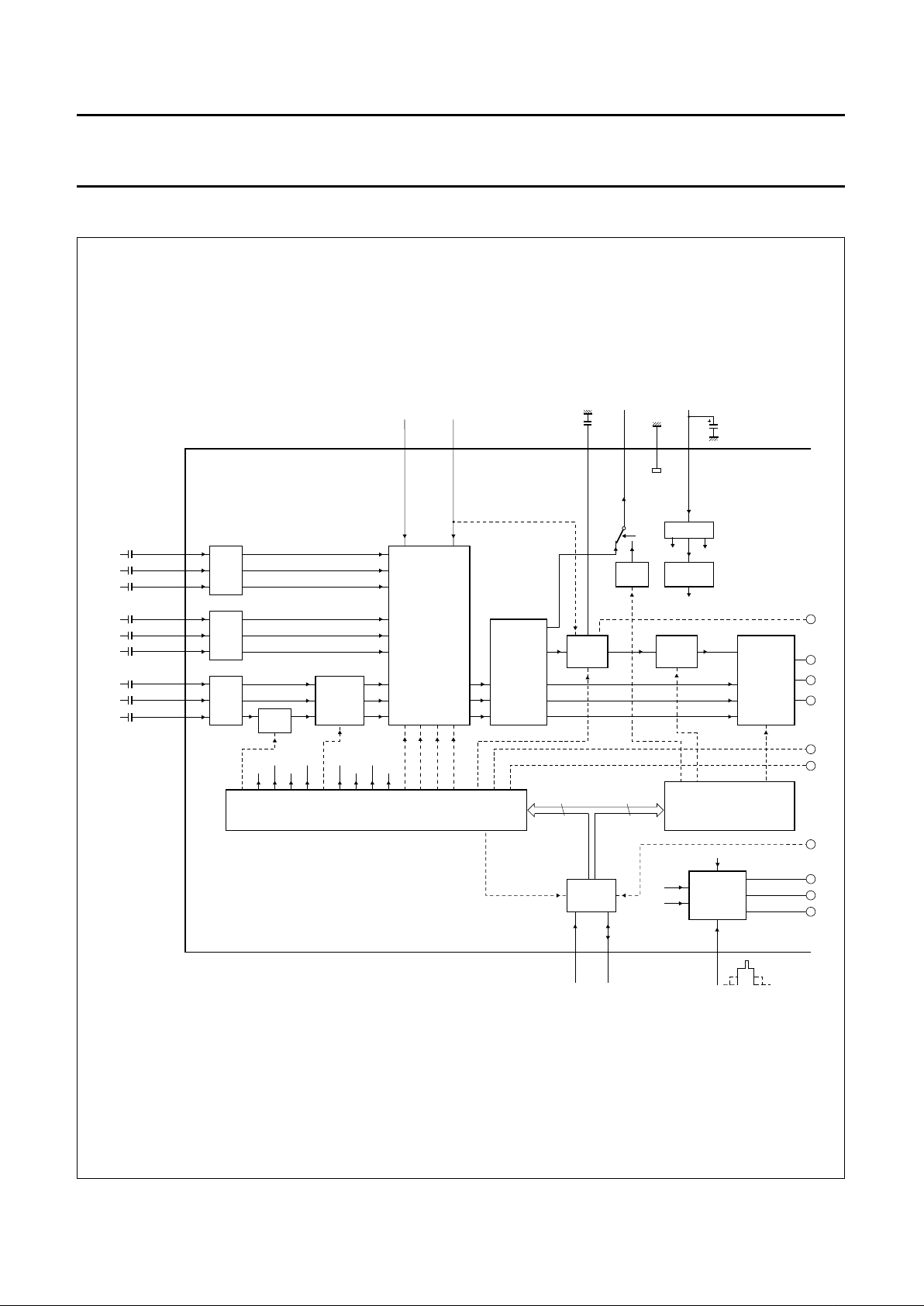
BLOCK DIAGRAM
Fig.1 Block diagram (continued in Fig.2).
handbook, full pagewidth
j
i
h
g
e
f
d
c
b
a
MGE875
200 µF
1 µF
CLAMP
TDA4780
CLAMP
CLAMP
0.45 V
1.43 V
PAL / SECAM
NTSC
MATRIX
INPUT
SELECTOR
FSON1
FSON2
FSDIS1
FSDIS2
Y - MATRIX
COLOUR
DIFFERENCE
MATRIX
ADAPTIVE
BLACK
Y
Y
Y
BL
GAMMA
Y
gamma
BL
SATURATION
ADJUST
HUE
ADJUST
BANDGAP
REFERENCE
SUPPLY
CONTROL REGISTERS
TCPL
RELC
BCOF
YEXHHDTV
FSBL
DELOF
SC5
YHI
REGISTERS
DIGITAL TO ANALOG CONVERTERS
I2C-BUS
RECEIVER
SANDCASTLE
DETECTOR
8 DATA
BREN
V
SC5
DELOF
B
G
R
CL
HV
(H)
NMEN
10
11
12
R
1
G
1
B
1
R
2
G
2
B
2
2
3
4
6
7
8
−(B − Y)
−(B − Y)
−(R − Y)
−(R − Y)
Y
Y
47 nF
10 nF
10 nF
10 nF
10 nF
10 nF
10 nF
10 nF
10 nF
13
FSW
1
FSW
2
FSW
1
FSW
2
1
18 26
C
PDST
YHUE
GND
9
5
V
P
U
GAP
14
SC
27
28
SCL
SDA
R
1
G
1
B
1
R
2
G
2
B
2
ADBL
R − Y
G − Y
B − Y
R
G
B
R
G
B
Y
YEXH
U
GAP
sandcastle input
I
2
C-bus
VP = 8 V
Y - output /
hue adjust
output
peak dark
storage
6 DATA
Page 5
1997 Feb 06 5
Philips Semiconductors Preliminary specification
RGB video processor with automatic
cut-off control and gamma adjust
TDA4780
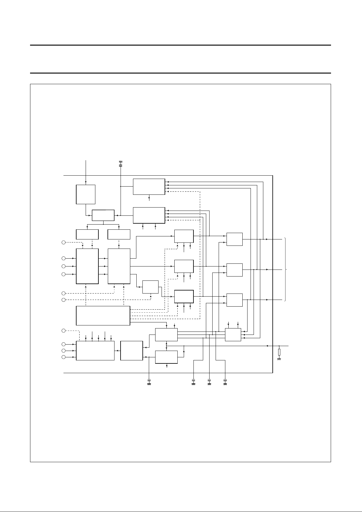
Fig.2 Block diagram (continued from Fig.1).
handbook, full pagewidth
j
i
h
g
e
f
d
c
b
a
MGE876
82 kΩ
1 µF
TDA4780
CONTRAST
ADJUST
BRIGHTNESS
ADJUST
REGISTERS
DIGITAL ANALOG CONVERTERS
TIMING
GENERATOR
B
G
R
B
B
B
G
R
FSBL
NMEN
HDTV
BLANK
MP
CL
HV
(H)
WHITE
POINT
ADJUST
MP
BLANK
WHITE
POINT
ADJUST
MP
BLANK
WHITE
POINT
ADJUST
MP
BLANK
BLUE
STRETCH
VOLTAGE
COMPARATOR
VOLTAGE
COMPARATOR
MINIMUM
DETECTOR
PEAK DRIVE
LIMITER
CUT-OFF RELATED
PEAK DRIVE
LIMITER
ABSOLUTE LEVEL
TCPL RELC
RELC
AVERAGE
BEAM
CURRENT
LIMITING
R
G
B
OUTPUT
BUFFER
OUTPUT
BUFFER
OUTPUT
BUFFER
1st AND 2nd
SWITCH-ON
DELAY
CUT-OFF
CONTROL
LEAKAGE
CURRENT
COMPARATOR
OUTPUT
CLAMP
BCL
15 16
C
PDL
24
22
20
R
O
G
O
B
O
19
CI
U
GAP
U
GAP
BCOF
BCOF
25
23
21
C
R
C
G
C
B
17
C
L
MOD2
220 nF
330 nF
220 nF 220 nF
cut-off storageleakage storage
leakage and
cut - off
current input
RGB
outputs
to
video
amplifiers
peak drive
limiting storage
average beam
current limiting
input
Page 6
1997 Feb 06 6
Philips Semiconductors Preliminary specification
RGB video processor with automatic
cut-off control and gamma adjust
TDA4780
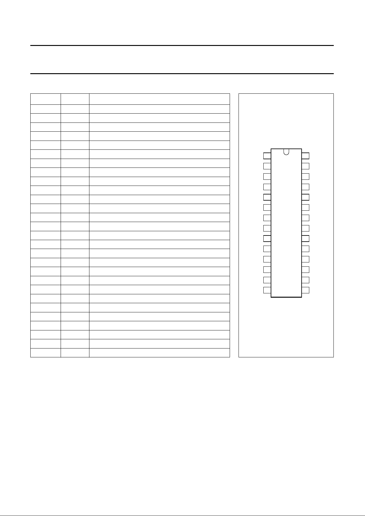
PINNING
SYMBOL PIN DESCRIPTION
FSW
2
1 fast switch 2 input
R
2
2 red input 2
G
2
3 green input 2
B
2
4 blue input 2
V
P
5 supply voltage
−(B − Y) 6 colour difference input −(B − Y)
−(R − Y) 7 colour difference input −(R − Y)
Y 8 luminance input
GND 9 ground
R
1
10 red input 1
G
1
11 green input 1
B
1
12 blue input 1
FSW
1
13 fast switch 1 input
SC 14 sandcastle pulse input
BCL 15 average beam current limiting input
C
PDL
16 storage capacitor for peak limiting
C
L
17 storage capacitor for leakage current compensation
C
PDST
18 storage capacitor for peak dark
CI 19 cut-off measurement input
B
O
20 blue output
C
B
21 blue cut-off storage capacitor
G
O
22 green output
C
G
23 green cut-off storage capacitor
R
O
24 red output
C
R
25 red cut-off storage capacitor
YHUE 26 Y-output/hue adjust output
SDA 27 I
2
C-bus serial data input/acknowledge output
SCL 28 I
2
C-bus serial clock input
Fig.3 Pin configuration.
page
FSW
2
R
2
G
2
B
2
V
P
−(B − Y)
−(R − Y)
Y
GND
R
1
G
1
B
1
FSW
1
SC
SCL
SDA
YHUE
C
R
C
G
G
O
R
O
C
B
B
O
CI
C
PDST
C
L
C
PDL
BCL
1
2
3
4
5
6
7
8
9
10
11
12
13
28
27
26
25
24
23
22
21
20
19
18
17
16
1514
TDA4780
MGE874
Page 7

1997 Feb 06 7
Philips Semiconductors Preliminary specification
RGB video processor with automatic
cut-off control and gamma adjust
TDA4780
FUNCTIONAL DESCRIPTION
Signal input stages
The TDA4780 contains 3 sets of input signal stages for:
1. Luminance/colour-difference signals:
a) Y: 0.45 V (p-p) VBS or 1.43 V (p-p) VBS,
selectable via I
2
C-bus.
b) −(R − Y): 1.05 V (p-p).
c) −(B − Y): 1.33 V (p-p).
The capacitively coupled signals are matrixed to
RGB signals by either a PAL/SECAM or NTSC matrix
(selected via I2C-bus).
2. (RGB)1signals (0.7 V (p-p) VB), capacitively coupled
(e.g. from external source).
3. (RGB)2signals (0.7 V (p-p) VB), capacitively coupled
(e.g. videotext, OSD).
All input signals are clamped in order to have the same
black levels at the signal switch input. Displayed signals
must be synchronous with the sandcastle pulse.
Signal switches
Both fast signal switches can be operated by switching
pins (e.g. SCART facilities) or set via the I
2
C-bus. With the
pin FSW1 the Y-CD signals or the (RGB)1signals can be
selected, with pin FSW2 the above selected signals or the
(RGB)2signals are enabled. During the vertical and
horizontal blanking time an artificial black level equal to the
clamped black level is inserted in order to clip off the sync
pulse of the luminance signal and to suppress hum during
the cut-off measurement time and eliminate noise during
these intervals.
Saturation, contrast and brightness adjust
Saturation, contrast and brightness adjusts are controlled
via the I
2
C-bus and act on Y, CD as well as on RGB input
signals. Gamma acts on the luminance content of the input
signals.
Gamma adjust
The gamma adjust stage has a non-linear transmission
characteristic according to the formula y = x
gamma
, where x
represents the input and y the output signal. If gamma is
smaller than unity, the lower parts of the signal are
amplified with higher gain.
Adaptive black (ADBL)
The adaptive black stage detects the lowest voltage of the
luminance component of the internal RGB signals during
the scanning time and shifts it to the nominal black level.
In order to keep the nominal white level the contrast is
increased simultaneously.
Blue stretch (BLST)
The blue stretch channel gets additional amplification if the
blue signal is greater than 80% of the nominal signal
amplitude. In the event the white point is shifted towards
higher colour temperature so that white parts of a picture
seem to be brighter.
Measurement pulse and blanking stage
During the vertical and horizontal blanking time and the
measurement period the signals are blanked to an ultra
black level, so the leakage current of the picture tube can
be measured and automatically compensated for.
During the cut-off measurement lines (one line period for
each R, G or B) the output signal levels are at cut-off
measurement level.
The vertical blanking period is timed by the sandcastle
pulse. The measurement pulses (leakage, R, G and B) are
triggered by the negative going edge of the vertical pulse
of the sandcastle pulse and start after the following
horizontal pulse.
The IC is prepared for 2f
H
(32 kHz) application.
Output amplifier and white adjust potentiometer
The RGB signals are amplified to nominal 2 V (p-p), the
DC-levels are shifted according to cut-off control.
The nominal signal amplitude can be varied by ±50% by
the white point adjustment via the I
2
C-bus (individually for
RGB respect).
Page 8

1997 Feb 06 8
Philips Semiconductors Preliminary specification
RGB video processor with automatic
cut-off control and gamma adjust
TDA4780
Automatic cut-off control
During leakage measurement time the leakage current is
compensated in order to get a reference voltage at the
cut-off measurement info pin. This compensation value is
stored in an external capacitor. During cut-off current
measurement times for the R, G and B channels, the
voltage at this pin is compared with the reference voltage,
which is individually adjustable via I2C-bus for each colour
channel. The control voltages that are derived in this way
are stored in the external feedback capacitors. Shift stages
add these voltages to the corresponding output signals.
The automatic cut-off control may be disabled via the
I
2
C-bus. In this mode the output voltage is clamped to
2.5 V. Clamping periods are the same as the cut-off
measurement periods.
Signal limiting
The TDA4780 provides two kinds of signal limiting.
First, an average beam limiting, that reduces signal level if
a certain average is exceeded. Second, a peak drive
limiting, that is activated if one of the RGB signals even
shortly exceeds a via I
2
C-bus adjusted threshold.
The latter can be either referred to the cut-off
measurement level of the outputs or to ground.
When signal limiting occurs, contrast is reduced, and at
minimum contrast brightness is reduced additionally.
Sandcastle decoder and timer
A 3-level detector separates the sandcastle pulse into
combined line and field pulses, line pulses, and clamping
pulses. The timer contains a line counter and controls the
cut-off control measurement.
Application with a 2-level 5 V sandcastle pulse is possible.
Switch on delay circuit
After switch on all signals are blanked and a warm up test
pulse is fed to the outputs during the cut-off measurement
lines. If the voltage at the cut-off measurement input
exceeds an internal level the cut-off control is enabled but
the signal remains still blanked. In the event of output
clamping, the cut-off control is disabled and the switch on
procedure will be skipped.
Y output and hue adjust
The TDA4780 contains a D/A converter for hue adjust.
The analog information can be fed, e.g. to the
multistandard decoder TDA4650 or TDA4655. This output
pin may be switched to a Y output signal, which can be
used for scan velocity modulation (SCAVEM). The Y
output is the Y input signal or the matrixed (RGB) input
signal according to the switch position of the fast switch.
I
2
C-bus
The TDA4780 contains an I2C-bus receiver for control
function.
ESD protection
The Pins are provided with protection diodes against
ground and supply voltage (see Chapter “Internal pin
configurations”). I
2
C-bus input pins do not shunt the
I2C-bus signals in the event of missing supply voltage.
EMC
The pins are protected against electromagnetic radiation.
Page 9

1997 Feb 06 9
Philips Semiconductors Preliminary specification
RGB video processor with automatic
cut-off control and gamma adjust
TDA4780
I2C-BUS RECEIVER
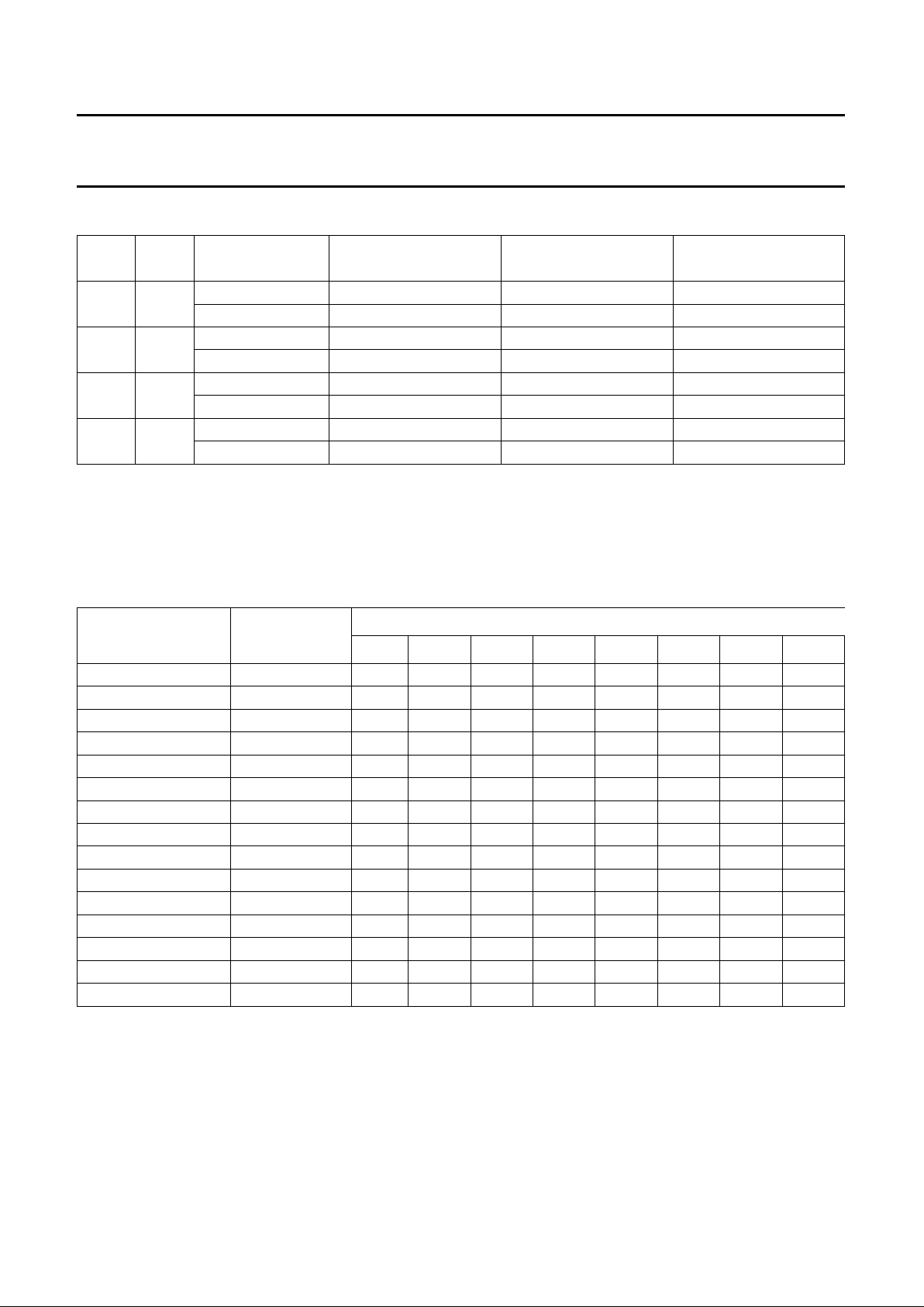
Table 1 Slave address; note 1
Note
1. Explanation for the cell contents of the table:
a) W means write.
Table 2 Slave receiver format (write mode; BREN = 0); note 1
Notes
1. Explanation for the cell contents of the table:
a) S means START condition.
b) P means STOP condition.
c) A means acknowledge.
2. All subaddresses within the range 00H to 0FH are automatically incremented. The subaddress counter wraps around
from 0FH to 00H. Only in this event 0FH will be acknowledged.
Subaddresses outside the range 00H to 0EH are not acknowledged by the device and neither auto-increment nor
any other internal operation takes place.
All eight bits of the subaddress have to be decoded by the device.
Table 3 Slave receiver format (write mode; BREN = 1); note 1
Notes
1. Explanation for the cell contents of the table:
a) S means START condition.
b) P means STOP condition.
c) A means acknowledge.
2. Auto-increment is not possible.
A6 A5 A4 A3 A2 A1 A0
W
10001000
S SLAVE ADDRESS A SUBADDRESS
(2)
A DATA BYTE
n data bytes with auto-increment of subaddresses
AP
S SLAVE ADDRESS A SUBADDRESS A DATA BYTE
(2)
AP
Page 10
1997 Feb 06 10
Philips Semiconductors Preliminary specification
RGB video processor with automatic
cut-off control and gamma adjust
TDA4780
Fig.4 The module address byte.
handbook, full pagewidth
ACKX
R/W
00100
module address
01
MSB LSB
MED696
handbook, full pagewidth
STOSAD
START
condition
data byte
STOP
condition
MADSTA
MED697
Fig.5 Data transmission without auto-increment (BREN = 0 or 1).
handbook, full pagewidth
SAD
START
condition
data byte
STOP
condition
MADSTA
MED698
STO
data bytes
Fig.6 Data transmission with auto-increment (BREN = 0)
Page 11

1997 Feb 06 11
Philips Semiconductors Preliminary specification
RGB video processor with automatic
cut-off control and gamma adjust
TDA4780
Table 4 Signal input selection and effect on adaptive black measurements by fast source switches and I2C-bus;
note 1
Note
1. Explanation for the cell contents of the table:
a) H = set to logic 1 or analog switch (pins 1 and 13) to >0.9 V.
b) L = set to logic 0 or analog switch (pins 1 and 13) to <0.4 V.
c) X = don’t care.
d) ON = this signal is selected.
I
2
C-BUS CONTROLLED BITS ANALOG SWITCH SELECTED SIGNALS
FSON2 FSDIS2 FSON1 FSDIS1
FSW2
(pin 1)
FSW1
(pin 13)
RGB
2
(pins 2, 3
and 4)
ADBL
RGB1 (pins 10,
11 and 12)
TV (pins 6,
7 and 8)
LLLLL L active ON
L H active ON
H X ON inactive
LLLHL X active ON
H X ON inactive
L L H X L X active ON
H X ON inactive
L H L L X L active ON
X H active ON
L H L H X X active ON
L H H X X X active ON
H L X X L X ON active
H ON inactive
H H X X X X ON active
Page 12
1997 Feb 06 12
Philips Semiconductors Preliminary specification
RGB video processor with automatic
cut-off control and gamma adjust
TDA4780
Table 5 Crosstalk; note 1
Note
1. Explanation for the cell contents of the table:
a) H = set to logic 1.
b) L = set to logic 0.
Table 6 Subaddress byte and data byte format; notes 1 and 2
Notes
1. Explanation for the cell contents of the table:
a) L = set to logic 0.
b) X means don’t care but for software compatibility with further video ICs with the same slave address, it is
recommended to set all these bits to logic 0.
2. After power on reset all alignment registers are set to 01H.
3. The least significant bit of the analog alignment register.
FSW1 FSW2 CROSSTALK
AT 4 MHz MAXIMUM
VALUE (dB)
AT 8 MHz MAXIMUM
VALUE (dB)
AT 13 MHz MAXIMUM
VALUE (dB)
L L RGB
1
→ Y, CD −58 −55 −50
RGB
2
→ Y, CD −58 −55 −50
L H Y, CD → RGB
1
−51 −50 −47
RGB
2
→ RGB
1
−58 −55 −50
L H Y, CD → RGB
2
−51 −50 −47
RGB
1
→ RGB
2
−58 −55 −50
H H Y, CD → RGB
2
−51 −50 −47
RGB
1
→ RGB
2
−58 −55 −50
FUNCTION SUBADDRESS
DATA BYTE
D7 D6 D5 D4 D3 D2 D1 D0
(3)
Brightness 00H L L A05 A04 A03 A02 A01 A00
Saturation 01H L L A15 A14 A13 A12 A11 A10
Contrast 02H L L A25 A24 A23 A22 A21 A20
Hue 03H L L A35 A34 A33 A32 A31 A30
Red gain 04H L L A45 A44 A43 A42 A41 A40
Green gain 05H L L A55 A54 A53 A52 A51 A50
Blue gain 06H L L A65 A64 A63 A62 A61 A60
Red level reference 07H L L A75 A74 A73 A72 A71 A70
Green level reference 08H L L A85 A84 A83 A82 A81 A80
Blue level reference 09H L L A95 A94 A93 A92 A91 A90
Peak drive limit 0AH L L AA5 AA4 AA3 AA2 AA1 AA0
Gamma 0BH L L AB5 AB4 AB3 AB2 AB1 AB0
Control register 1 0CH SC5 DELOF BREN X NMEN X X X
Control register 2 0DH X HDTV FSBL BCOF FSDIS2 FSON2 FSDIS1 FSON1
Control register 3 0EH ADBL YHI MOD2 BLST YEXH RELC TCPL L
Page 13

1997 Feb 06 13
Philips Semiconductors Preliminary specification
RGB video processor with automatic
cut-off control and gamma adjust
TDA4780
Table 7 RGB processor mode bits control register
SYMBOL PARAMETER CONDITIONS
Control register 1
SC5 sandcastle 5 V 0 = 3-level sandcastle pulse
1 = 2-level sandcastle pulse
DELOF delay of leading edge of
clamping pulse switched off
0 = delay
1 = no delay
BREN buffer register enable 0 = new data are executed just after reception
1 = data is held in a latch (buffer register) and will be transferred to their
destination register within the next vertical blanking interval; the device
does not acknowledge any new data transfer until the internal transfer to
the destination register has been completed
NMEN NTSC matrix enable; note 1 0 = PAL matrix
1 = NTSC matrix; hue position set on −2 degrees
Control register 2
HDTV HDTV / progressive scan for
ADBL line counter
0 = 272 (PAL), 224 (NTSC) lines
1 = 544 (PAL), 448 (NTSC) lines
FSBL full screen black level, e.g. for
optical measurement
0 = normal mode
1 = cut-off measurement level during full field, brightness inactive
BCOF internal black level control off 0 = automatic cut-off control active
1 = RGB outputs clamped to fixed DC levels
FSON2 fast switch 2 on see Table 4
FSDIS1 fast switch 1 disable
FSDIS2 fast switch 2 disable
FSON1 fast switch 1 on
Control register 3
ADBL adaptive black 0 = off
1=on
YHI Y high level 0 = input = 0.315 V (p-p) (black-white)
1 = input = 1.0 V (p-p) (black-white)
MOD2 modus 2 0 = inactive;
(BCOF = 0) AND (MOD2 = 1) is senseless, no output stabilization
1 = output clamp without brightness adjust, brightness remains active
e.g. for blue stretch
BLST blue stretch 0 = off
1=on
YEXH Y exclusive hue 0 = pin 26 is switched to hue adjust output
1 = pin 26 is switched to Y output
RELC relative to cut-off 0 = peak drive limit to absolute output
1 = peak drive limit relative to cut-off
TCPL time constant peak drive limiter 0 = 2f
H
1=1f
H
Page 14
1997 Feb 06 14
Philips Semiconductors Preliminary specification
RGB video processor with automatic
cut-off control and gamma adjust
TDA4780
Note
1. Matrix coefficients should be tested by comparing RGB output signals with a reference RGB colour bar, which is fed
in at (RGB)1 or (RGB)2 inputs. In the event of NMEN = 1 (NTSC) at minimum saturation the Y output and RGB output
signals are not identical to the Y input signal. PAL/SECAM signals are matrixed by the equation:
V
G −Y
= −0.51V
R − Y
− 0.19V
B − Y
NTSC signals are matrixed by the equations (hue phase shift of −2 degrees):
V
R − Y*
= 1.39V
R − Y
− 0.07V
B − Y
; V
G − Y*
= −0.46V
R − Y
− 0.15V
B − Y
; V
B − Y*=VB−Y
For demodulation axis see Fig.11.
In the matrix equations: V
R − Y
and V
B − Y
are conventional PAL demodulation axes and amplitudes at the output of
the demodulator. V
R − Y*
, V
G − Y*
and V
B − Y*
are the NTSC-modified colour-difference signals.
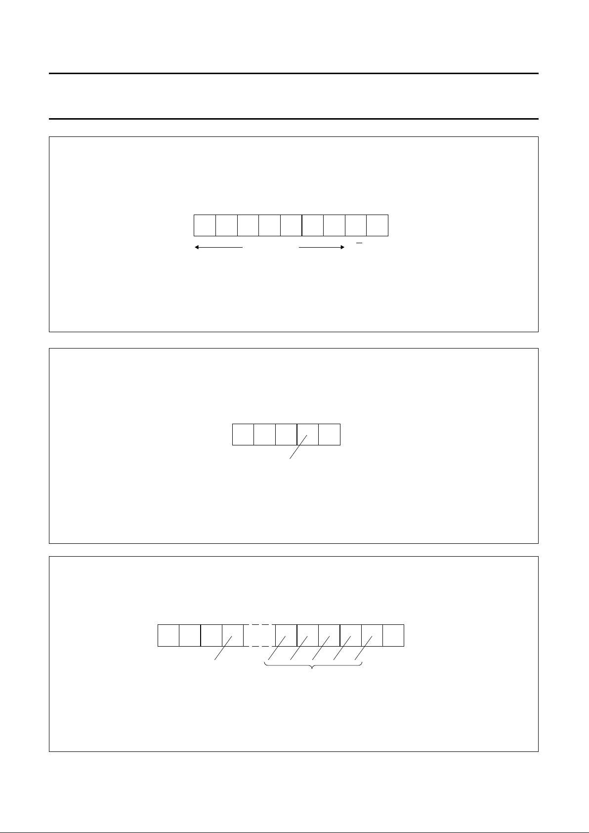
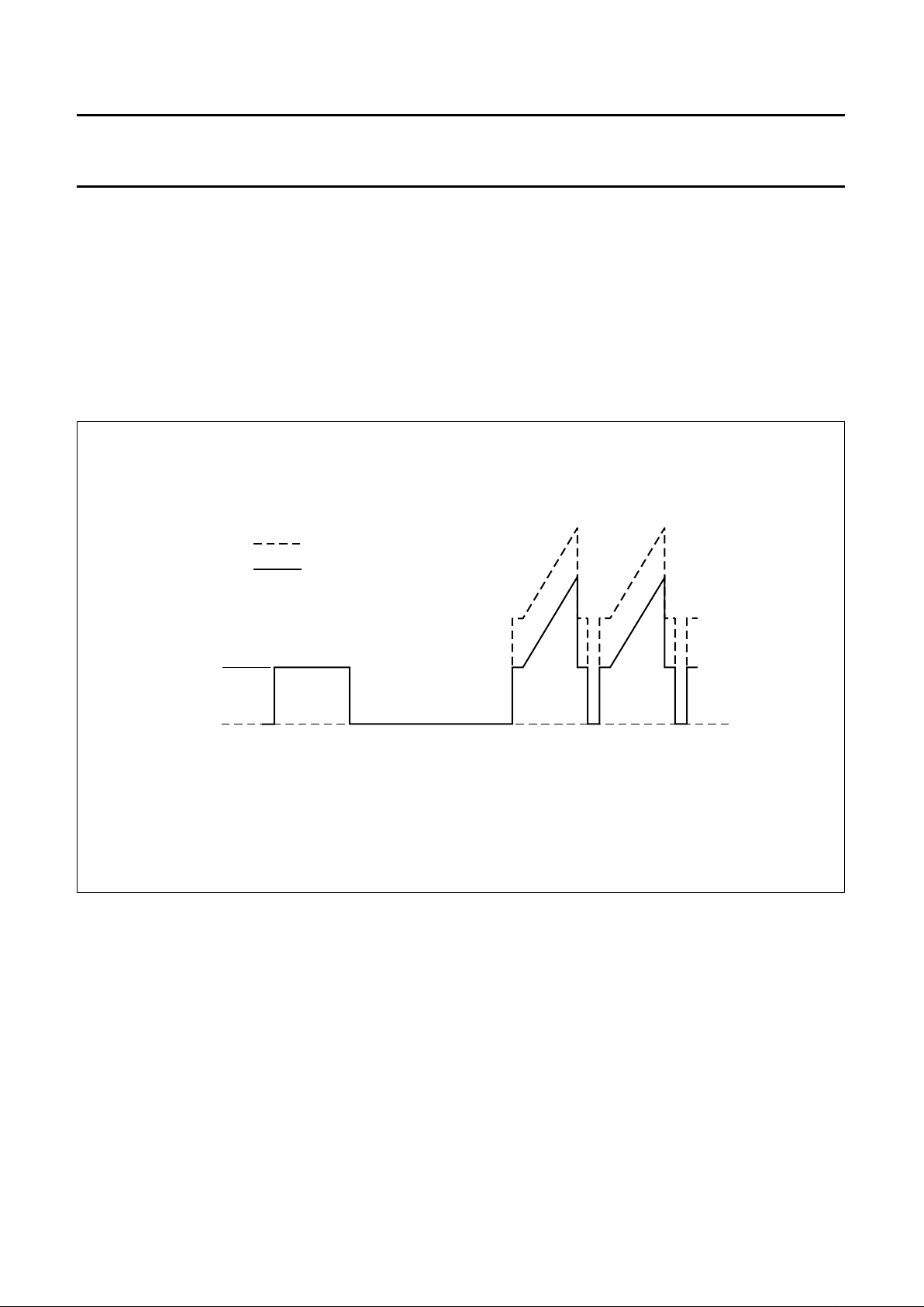
Fig.7 Cut-off measurement pulses.
handbook, full pagewidth
MGE878
maximum brightness
nominal brightness
ultra-black
cut-off measurement line
for green signal
Page 15

1997 Feb 06 15
Philips Semiconductors Preliminary specification
RGB video processor with automatic
cut-off control and gamma adjust
TDA4780
Fig.8 Principle of adaptive black control.
handbook, full pagewidth
MGE879
adaptive black level controlinput signal
nominal white
level
nominal black
level
Fig.9 Principle of blue stretch.
handbook, full pagewidth
MGE880
R
G
B
Page 16

1997 Feb 06 16
Philips Semiconductors Preliminary specification
RGB video processor with automatic
cut-off control and gamma adjust
TDA4780
handbook, full pagewidth
MGE881
LM
sandcastle pulse with vertical component
timing controlled by sandcastle pulse
R channel
G channel
B channel
MR
MG
MB
LM
LM
MT
DG
Fig.10 Pulse diagram.
LM = leakage current measurement time.
MR, MG, MB = R, G, B cut-off measurement pulses.
MT = measurement time.
DG = internal blanking.
Fig.11 Demodulation axes.
handbook, full pagewidth
MGE877
V-axis
V-axis
U-axis
(B − Y)
2.03 / 0˚
U-axis
(B − Y)
2.03 / 0˚
(R − Y)
1.14 / 90˚
(G − Y)
0.698 / 236.4˚
(R − Y)
1.59 / 95.1˚
(G − Y)
0.606 / 239.9˚
PAL
NTSC-JAPAN
nominal hue = −2˚
Page 17

1997 Feb 06 17
Philips Semiconductors Preliminary specification
RGB video processor with automatic
cut-off control and gamma adjust
TDA4780
LIMITING VALUES
In accordance with the Absolute Maximum Rating System (IEC 134).
Note
1. Charge device model class A: discharging a 200 pF capacitor through a 0 Ω series resistor.
THERMAL CHARACTERISTICS
QUALITY SPECIFICATION
In accordance with URV-4-2-59/601. The number of the quality specification can be found in the
“Quality Reference
Handbook
”. The handbook can be ordered using the code 9397 750 00192.
SYMBOL PARAMETER CONDITIONS MIN. MAX. UNIT
V
P
supply voltage −0.1 +9.0 V
V
10, 11, 12
(RGB)1 inputs with respect to GND −0.1 V
P
V
V
2, 3, 4
(RGB)2 inputs with respect to GND −0.1 V
P
V
V
8, 7, 6
Y, CD-inputs with respect to GND −0.1 V
P
V
V
13, 1
switch 1 and switch 2 input voltage with respect to GND −0.1 V
P
V
V
25, 23, 21, 17
black level, leakage storage with respect to GND −0.1 V
P
V
V
14
sandcastle with respect to GND −0.7 VP+ 5.8 V
V
15
average current information with respect to GND −0.7 VP+ 0.7 V
V
16
peak drive storage with respect to GND −0.1 V
P
V
V
18
peak dark storage with respect to GND −0.1 V
P
V
V
19
cut-off control input voltage with respect to GND −0.7 VP+ 0.7 V
V
27, 28
I2C-bus: SDA and SCL voltage with respect to GND −0.1 V
P
V
I
24, 22, 20
output peak current −20 − mA
I
24, 22, 20
output average current −10 − mA
I
26
Y output/hue adjust current −8 − mA
P
tot
total power dissipation − 1200 mW
T
amb
operating ambient temperature −20 +70 °C
T
stg
storage temperature −20 +150 °C
V
es
electrostatic handling; note 1 −500 +500 V
SYMBOL PARAMETER VALUE UNIT
R
th j-a
thermal resistance from junction to ambient in free air 47 K/W
Page 18

1997 Feb 06 18
Philips Semiconductors Preliminary specification
RGB video processor with automatic
cut-off control and gamma adjust
TDA4780
CHARACTERISTICS
V
P
=8V; T
amb
= +25 °C; V
nom
: nominal signal amplitude (black-white) 2 000 mV (peak-to-peak value) at output pins;
gamma = 1; adaptive black inactive; brightness, contrast, saturation and white balance at nominal settings; no beam
current or peak drive limiting; all voltages are related to ground (pin 9) and measured in Figs 1 and 2; unless otherwise
specified.
SYMBOL PARAMETER CONDITIONS MIN. TYP. MAX. UNIT
V
P
supply voltage (pin 5) 7.2 8 8.8 V
I
P
supply current (pin 5) − 100 120 mA
Colour-difference inputs (−(B − Y): pin 6, −(R − Y): pin 7; capacitively coupled to a low-ohmic source;
recommendation: maximum 600 Ω)
V
6(p-p)
−(B − Y) signal (peak-to-peak value) 75% colour bar signal − 1.33 − V
V
6, 7
internal bias during clamping − 4.0 − V
I
6, 7
DC input current between clamping
pulses
−− 0.1 µA
I
6, 7
maximum input current during clamping 100 180 260 µA
V
7(p-p)
−(R − Y) signal (peak-to-peak value) 75% colour bar signal − 1.05 − V
R
6, 7
AC input resistance 10.0 −−MΩ
Y input (pin 8; capacitively coupled to a low-ohmic source; recommendation: maximum 600 Ω)
V
8(p-p)
input signal (composite signal; VBS;
peak-to-peak value)
adaption to two
different signal levels
via control bit YHI
YHI = 0 − 0.45 − V
YHI = 1 − 1.43 − V
R
8
AC input resistance 10.0 −−MΩ
V
8
internal bias during clamping YHI = 0 − 3.7 − V
YHI = 1 − 4.6 − V
I
8
DC input current between clamping
pulses
−− 0.1 µA
I
8(max)(clamp)
maximum input current during clamping 100 180 260 µA
RGB input 1 (R
1
: pin 10, G1: pin 11, B1: pin 12; capacitively coupled to a low-ohmic source;
recommendation: maximum 600 Ω); note 1
V
10, 11, 12(p-p)
input signal (peak-to-peak value) − 0.7 − V
R
10, 11, 12
AC input resistance 10.0 −−MΩ
V
10, 11, 12
internal bias during clamping − 5.1 − V
I
10, 11, 12
DC input current between clamping
pulses
−− 0.1 µA
I
10, 11, 12(clamp)
maximum input current during clamping 100 180 260 µA
Page 19

1997 Feb 06 19
Philips Semiconductors Preliminary specification
RGB video processor with automatic
cut-off control and gamma adjust
TDA4780
RGB input 2 (R2: pin 2, G2: pin 3, B2: pin 4; capacitively coupled to a low-ohmic source;
recommendation: maximum 600 Ω); note 1
V
2, 3, 4(p-p)
input signal (peak-to-peak value) − 0.7 − V
R
2, 3, 4
AC input resistance 10.0 −−MΩ
V
2, 3, 4
internal bias during clamping − 5.1 − V
I
2, 3, 4
DC input current between clamping
pulses
−− 0.1 µA
I
2, 3, 4(max)(clamp)
maximum input current during clamping 100 180 260 µA
Fast signal switches and blanking (fast signal switch 1 (pin 13); Y, CD / R
1
, G1, B1; control bits FSDIS1,
FSON1)
V
13
voltage to select Y and CD − 0 0.4 V
V
13
voltage range to select R1, G1 and B
1
0.9 1.0 5.5 V
R
13
internal resistor to ground 3.3 3.8 4.8 kΩ
CROSSTALK (SEE TABLE 5)
t
s
− t
i
difference between transit times for
signal switching and signal insertion
−− 10 ns
Fast signal switch 2 (pin 1; Y, CD or R
1
, G1, B1 / R2, G2, B2; control bits FSDIS2, FSON2)
V
1
voltage to select Y and CD / R1, G1 and
B
1
− 0 0.4 V
V
1
voltage range to select R2, G2 and B
2
0.9 1.0 5.5 V
V
1
required minimal voltage to switch off the
ADBL measurement
− 0.87 1.0 V
R
1
internal resistor to ground R1>R
13
2.8 4.2 6.0 kΩ
CROSSTALK (SEE TABLE 5)
t
s
− t
i
difference between transit times for
signal switching and signal insertion
−− 10 ns
Adjust stages (adaptive black, gamma, contrast, saturation, brightness and white point adjust, blue stretch)
A
DAPTIVE BLACK (DETECTORS INACTIVE STATUS DUE TO ACTION OF FAST SWITCH 2(PIN 1); see Table 4, Fig.9 and note 2)
I
18(dch)
discharge current of peak dark storage
capacitor
outside active
measurement window
−1.0 0.0 +1.0 µA
inside active
measurement window
1.5 2.5 3.5 µA
I
18(ch)
charge current of peak dark storage
capacitor
−360 −300 −250 µA
d
bl(max)
maximum level shift: ∆ black level in
percent of nominal signal amplitude
10 13 16 %
d
bl(nom)
difference between nominal black and
adaptive black in percent of nominal
signal amplitude
−3 0 +3 %
t
dibb
detectors inactive time before blanking 2.3 3.1 4.0 µs
t
diab
detectors inactive time after blanking 2.3 2.5 3.4 µs
SYMBOL PARAMETER CONDITIONS MIN. TYP. MAX. UNIT
Page 20

1997 Feb 06 20
Philips Semiconductors Preliminary specification
RGB video processor with automatic
cut-off control and gamma adjust
TDA4780
GAMMA ADJUST (ACTS ON INTERNAL Y SIGNAL;YMATRIX SEE Y OUTPUT;I2C-BUS CONTROLLED POTENTIOMETER
(SUBADDRESS 0BH); RESOLUTION 6 BIT; note 3)
d
g
range of gamma
minimum (3FH) − 0.7 −−
maximum (00H) − 1.0 −−
G
max
maximum gain at minimum gamma near nominal black 5 6 7 dB
SATURATION ADJUST (ACTS ON RGB SIGNALS;YMATRIX SEE Y OUTPUT;I2C-BUS CONTROLLED POTENTIOMETERS
(SUBADDRESS 01H); RESOLUTION 1.5% OF MAXIMUM SATURATION)
d
s(max)
maximum saturation I2C-bus data 3FH;
measured at 100 kHz;
relative to nominal
saturation; note 4
4.7 5.2 5.8 dB
d
s(min)
minimum saturation I2C-bus data 00H;
measured at 100 kHz;
relative to typical value
of maximum saturation
−− −50 dB
CONTRAST ADJUST (ACTS ON RGB SIGNALS;I2C-BUS CONTROLLED POTENTIOMETERS (SUBADDRESS 02H); RESOLUTION
1.5% OF MAXIMUM CONTRAST)
d
c(max)
maximum contrast I2C-bus data 3FH;
limiters inactive;
relative to nominal
contrast; note 5
− 4.5 5.5 dB
d
c(min)
minimum contrast I2C-bus data 00H;
relative to maximum
contrast
−28 −22 −16 dB
BRIGHTNESS ADJUST (ACTS ON RGB SIGNALS;I2C-BUS CONTROLLED POTENTIOMETERS (SUBADDRESS 00H); RESOLUTION
1.5% OF RANGE; ∆ BLACK LEVEL IN PERCENT OF NOMINAL SIGNAL AMPLITUDE REFERRED TO CUT-OFF MEASURING LEVEL)
d
br(max)
maximum brightness: ∆ black level I2C-bus data 3FH 23 30 37 %
d
br(nom)
nominal brightness: ∆ black level I2C-bus data 29H −7 0 +7 %
d
br(min)
minimum brightness: ∆ black level I2C-bus data 00H −58 −50 −42 %
d
br(max)
maximum brightness: ∆ black level I2C-bus data 3FH;
control bits BCOF = 1
and MOD2 = 0
23 30 37 %
d
br(min)
minimum brightness: ∆ black level I2C-bus data 00H;
control bits BCOF = 1
and MOD2 = 0
−58 −50 −42 %
BLUE STRETCH (BLUE STRETCH IS ACTIVATED BY I2C-BUS CONTROL BIT BLST = 1; see Fig.9)
G
bs
increase of small signal gain 100% of nominal signal
amplitude and at 1 MHz
15 20 25 %
SYMBOL PARAMETER CONDITIONS MIN. TYP. MAX. UNIT
Page 21

1997 Feb 06 21
Philips Semiconductors Preliminary specification
RGB video processor with automatic
cut-off control and gamma adjust
TDA4780
DIFFERENCES OF BLACK LEVEL STEPS (DIFFERENCES FROM CHANNEL TO CHANNEL OF THE RATIO OF THE DIFFERENCE
(BLACK LEVEL CUT-OFF MEASUREMENT LEVEL) TO ACTUAL NOMINAL SIGNAL AMPLITUDE (V
NOM24,VNOM22,VNOM20
) OVER THE
WHOLE CONTRAST
, BRIGHTNESS AND SATURATION RANGE, SWITCHING MATRIX OR SWITCHING FAST SWITCHES, GAMMA =1,
BLST = 0, ADBL = 0)
∆V/V
nom
static deviation note 6; ripple on pin 5
during clamping ≤1mV;
note 7
−1.0 − +1.0 %
at nominal saturation −0.5 − +0.5 %
RGB outputs (output for positive RGB signals (R: pin 24, G: pin 2, B: pin 20); following data without external
load)
R
24, 22, 20
differential output resistance − 25 30 Ω
I
24, 22, 20(max)
maximum output current 4.0 5.0 − mA
V
24, 22, 20(min)
minimum output voltage note 8 −− 0.8 V
V
24, 22, 20(max)
maximum output voltage RL≥ 2kΩ 6.3 7.0 − V
V
24, 22, 20(max)(p-p)
maximum signal amplitude (black-white)
due to internal limits
(peak-to-peak value)
3.3 −−V
V
24, 22, 20(max)(p-p)
nominal signal amplitude (black-white;
peak-to-peak value)
at nominal white adjust,
contrast and saturation
setting; gamma = 1;
nominal input signals
1.7 2.0 2.3 V
V
24, 22, 20
cut-off measurement level note8 1.0 − 5.0 V
V
24, 22, 20
recommended cut-off measurement
level
− 3.0 − V
OUTPUT CLAMPING (RGB)
V
20, 22, 24
clamp voltage black level control bit BCOF = 1 2.3 2.5 2.7 V
WHITE POTENTIOMETERS
∆G
v(inc)(max)
maximum increase of AC gain I2C-bus data 3FH;
relative to nominal
setting; note 9
40 50 60 %
∆G
v(dec)(max)
maximum decrease of AC gain I2C-bus data 00H;
relative to nominal
setting; note 9
40 50 60 %
SYMBOL PARAMETER CONDITIONS MIN. TYP. MAX. UNIT
Page 22

1997 Feb 06 22
Philips Semiconductors Preliminary specification
RGB video processor with automatic
cut-off control and gamma adjust
TDA4780
OVERALL WHITE POINT DEVIATION
∆V/V
nom
note 10 input: (RGB)
1, 2
;
differences from
channel to channel of
the ratio of the
difference (signal white
level cut-off
measurement level) to
actual nominal signal
amplitude (V
nom24
,
V
nom22
, V
nom20
) over the
whole saturation range
at nominal contrast,
brightness and nominal
input signals; ripple on
pin 5 during clamping
≤1 mV; note 7
−2.0 − +2.0 %
Frequency behaviour
B
ETWEEN THE Y INPUT (PIN 8) AND THE RGB OUTPUTS (PINS 24, 22 AND 20)
∆G decrease in gain 1 MΩ and 20 pF load at
13 MHz
−− 3dB
B
ETWEEN THE COLOUR-DIFFERENCE INPUTS (PINS 7 AND 6) AND THE CORRESPONDING R AND B OUTPUTS (PINS 24 AND 20)
∆G decrease in gain at 13 MHz −− 3dB
B
ETWEEN THE (RGB)
1, 2
INPUTS (PINS 10, 11 AND 12 OR 2, 3 AND 4) AND THE RGB OUTPUTS (PINS 24, 22 AND 20)
∆G decrease in gain at 22 MHz −− 3dB
Sandcastle input (pin 14; control bit SC5); note 11
I
14
input current V14< 0.5 V −100 −−µA
C
14-9
input capacitance −− 10 pF
V
14
required voltage range
for horizontal and vertical blanking
pulses
SC5 = 0 or SC5 = 1 2.0 2.5 3.0 V
for horizontal pulses (line count) SC5 = 0 4.0 4.5 4.9 V
for burst key pulses SC5 = 0 6.1 − V
P
+
5.8
V
for burst key pulses and line count SC5 = 1 4.0 − V
P
+
5.8
V
SYMBOL PARAMETER CONDITIONS MIN. TYP. MAX. UNIT
Page 23

1997 Feb 06 23
Philips Semiconductors Preliminary specification
RGB video processor with automatic
cut-off control and gamma adjust
TDA4780
CLAMP PULSE DELAY
T
d(clamp)
delay of leading edge of clamping pulse nominal sandcastle
pulse
DELOF = 0 1.2 1.5 1.8 µs
DELOF = 1 − 0 −µs
R
EQUIRED MINIMAL BURST GATE PULSE WIDTH
t
W
DELOF = 0 line frequency: 16 kHz 3 −−µs
DELOF = 1 line frequency: 32 kHz 1.5 −−µs
Generation of measurement lines and blanking; note 12
∆V/V
nom
∆V = VCL − VUB
difference between ultra black level
(VUB) and measurement level (VCL) in
percent of nominal signal amplitude
no clipping;
independent of white
point adjust
25 35 45 %
WARM UP TEST PULSE DURING MT (see pulse diagram Fig.10)
V
WU
warm up level VWU=VPL− 1V;
VPL= peak drive level
(see also signal
limiting); given by
I2C-bus; subaddress
0AH; no warm up test
pulse in the event of
output clamping
(BCOF = 1)
−− −−
V
WU(max)
maximum warm up level I2C-bus data 3FH;
RELC = 0
6.3 6.6 6.9 V
V
WU(fixed)
fixed warm up level RELC = 1 5.0 5.2 5.4 V
THRESHOLD FOR POWER ON RESET (POR) DURING TIME DG (see pulse diagram Fig.10)
V
20, 22, 24(POR)
output voltage to cause POR RELC = 0 − V
PL
− V
RELC = 1 − 5.7 − V
Y output (pin 26; note 13)
V
26(nom)(p-p)
nominal signal amplitude (black-white;
independent of gamma, adaptive black,
saturation, contrast and brightness;
peak-to-peak value)
control bit YEXH = 1;
hue DAC (subaddress
03H) set to >28H
0.85 1.0 1.15 V
V
26
black level YEXH = 1; I2C-bus
data 3FH
− 4.0 − V
YEXH = 1; I
2
C-bus
data 20H
− 2.0 − V
a
r
Y matrix coefficients Y = arR+agG+abB 0.27 0.30 0.33
a
g
Y matrix coefficients Y = arR+agG+abB 0.53 0.59 0.65
a
b
Y matrix coefficients Y = arR+agG+abB 0.10 0.11 0.12
SYMBOL PARAMETER CONDITIONS MIN. TYP. MAX. UNIT
Page 24

1997 Feb 06 24
Philips Semiconductors Preliminary specification
RGB video processor with automatic
cut-off control and gamma adjust
TDA4780
R
26
differential output resistance − 190 230 Ω
∆τ
26
group delay time between RGB outputs
and Y output
20 25 30 ns
f
g
3 dB bandwidth 11 15 − MHz
Automatic cut-off control (pin 19; measurement periods see beam info on pin 19)
V
19
permissible voltage (also during
scanning period)
−− V
P
−
1.4
V
V
REF0
internally controlled voltage on pin 19 during leakage
measurement time LM
2.4 2.7 3.0 V
I
o19(max)
maximum output current −350 −−250 µA
I
i19(max)
maximum input current 250 − 350 µA
R
19
input resistance for measurement input 1 −−MΩ
I
19
additional input current only during warm up − 0.5 − mA
V
19
threshold of warm up detector (active in
line MG)
4.3 4.5 4.7 V
V
MEAS
difference between input voltage for
cut-off and V
REF0
; adjustable via I2C-bus
(subaddress for reference: R: 07H,
G: 08H and B: 09H)
−− −−
maximum V
MEAS
I2C-bus data 3FH 1.45 1.6 1.75 V
nominal V
MEAS
I2C-bus data 20H 0.9 1.0 1.1 V
minimum V
MEAS
I2C-bus data 00H 0.4 0.45 0.5 V
Storage of cut-off control voltage / output clamping voltage (pins 25, 23 and 21)
I
25, 23, 21
input currents of storage inputs outside
of the measurement time
−− 0.1 µA
I
25, 23, 21(max)
maximum charge / discharge current
during measurement time
0.2 0.3 0.4 mA
G
stg
gain from storage pins 25, 23 and 21 to
outputs
− 1.7 −−
Storage of leakage information (pin 17)
I
17
maximum charge / discharge current at
time LM
300 400 −µA
I
17
discharge current peak limiting during time
MK active
− 4 − mA
I
17
leakage current outside time LM −− 0.1 µA
V
17
voltage to reset IC to switch on
conditions
V17 is below 2.3 2.5 3.0 V
SYMBOL PARAMETER CONDITIONS MIN. TYP. MAX. UNIT
Page 25

1997 Feb 06 25
Philips Semiconductors Preliminary specification
RGB video processor with automatic
cut-off control and gamma adjust
TDA4780
Signal limiting (the limitation acts on contrast and at low contrast on brightness)
AVERAGE BEAM CURRENT LIMITING (PIN 15)
V
15
start of contrast reduction − 4 − V
∆V
15
input range for full contrast reduction −−2−V
V
15
start of brightness reduction − 2.5 − V
∆V
15
input range for full brightness reduction −−1.6 − V
I
15
input current −− −0.5 µA
PEAK SIGNAL LIMITING OF OUTPUT SIGNALS (PIN 16; THE LIMITATION ACTS 1H DELAYED; LIMITING LEVEL ADJUSTABLE BY
I2C-BUS (SUBADDRESS 0AH; CONTROL BIT RELC = 0))
V
24, 22, 20(max)
maximum limiting level extrapolated from 2FH 6.8 − 7.2 V
V
24, 22, 20(min)
minimum limiting level I2C-bus data 00H − 2.3 3 V
I
16(max)
maximum discharge current at peak
drive
RELC = 0 4 − 6mA
PEAK SIGNAL LIMITING (PIN 16; CONTROL BIT RELC = 1; LIMITING LEVEL (V
LIL
) ADJUSTABLE BY I2C-BUS (SUBADDRESS 0AH))
V
LiL
equal gain in white point
adjust; signal only in
one output channel;
peak drive limiting
starts, if the maximum
of the RGB signals
after white point
adjustment exceeds a
threshold
maximum limiting level I
2
C-bus data 3FH 3.2 3.5 4.0 V
minimum limiting level I
2
C-bus data 00H 1.2 1.5 1.8 V
DISCHARGE CURRENTS (CUT-OFF MEASUREMENT LEVEL MX = MR OR MB OR MG)
I
16(tot)(dch)
total discharge current I16=I
16(1)+I16(2)+I16(3)
−− −−
Threshold 1 (TH1)
I
16(1)(max)(dch)
maximum discharge current TH1 = MX + V
LiL
; 1 line
delayed and low-pass
filtered
4.5 6 7.5 mA
S steepness − 15 − mA/V
Low-pass filter, control bit TCPL
t
DPDL
time constant low-pass filter TCPL = 1 (at 1fH);
RELC = 1
0.9 1.2 1.5 µs
t
DPDL
time constant low-pass filter TCPL = 0 (at 2fH);
RELC = 1
0.4 0.6 0.8 µs
Threshold 2 (TH2)
I
16(2)(max)(dch)
maximum discharge current TH2 = MX + V
LiL
× 1.10;
1 line delayed
4.5 6 7.5 mA
S steepness − 15 − mA/V
SYMBOL PARAMETER CONDITIONS MIN. TYP. MAX. UNIT
Page 26

1997 Feb 06 26
Philips Semiconductors Preliminary specification
RGB video processor with automatic
cut-off control and gamma adjust
TDA4780
Threshold 3 (TH3)
I
16(3)(max)(dch)
maximum discharge current TH3 = MX + V
LiL
;
undelayed
0.45 0.6 0.75 mA
S steepness − 1.5 − mA/V
C
HARGE CURRENT
I
16
charge current −2 −1 −0.5 µA
V
16
start of contrast reduction − 4 − V
∆V
16
input range for full contrast reduction −−2−V
V
16
start of brightness reduction − 2.5 − V
∆V
16
input range for full brightness reduction −−1.6 − V
V
16(max)
maximum voltage by internal limitation 4.5 −−V
Hue adjust output (pin 26); note 14
V
o26(min)
minimum output voltage YEXH = 0; I2C-bus
data 00H
0.5 − 1.0 V
V
o26(nom)
nominal output voltage YEXH = 0; I2C-bus
data 20H
3.0 3.2 3.4 V
V
o26(max)
maximum output voltage YEXH = 0; I2C-bus
data 3FH
4.8 − 5.6 V
I
26
current of internal emitter follower 500 700 −µA
I
2
C-bus inputs
f
28
clock frequency range 0 − 100 kHz
t
SU;DAT
data set-up time 250 −−ns
t
H
clock pulse HIGH 4 −−µs
t
L
clock pulse LOW 4.7 −−µs
t
r
rise time −− 1µs
t
f
fall time −− 0.3 µs
Input levels (pins 27 and 28)
V
IL
LOW level input voltage −− 1.5 V
V
IH
HIGH level input voltage 3.0 − 5.5 V
I
I
input current V27and V28= 0.4 V −10 −−µA
V
27
and V28= 0.9V
P
−− 10 µA
Output level (pin 27)
V
OL
LOW level output voltage −− 0.4 V
I
O
output current V27= 0.4 V 3.0 −−mA
SYMBOL PARAMETER CONDITIONS MIN. TYP. MAX. UNIT
Page 27

1997 Feb 06 27
Philips Semiconductors Preliminary specification
RGB video processor with automatic
cut-off control and gamma adjust
TDA4780
Notes to the characteristics
1. RGB signals controlled by saturation, adaptive black, contrast and brightness. Gamma affects the Y component of
the internal RGB signals.
2. Adaptive black control acts on Y signal, which is either Y input or Y output from RGB matrix. Negative set-up is not
affected. The level shift value is determined by the peak dark detector, operation selected by control bit ADBL. The
peak dark detector is inactive during blanking. Peak dark detector activated by internal line counter, which starts after
the end of the vertical blank of the sandcastle. Active from line 16 (after end of vertical sandcastle) to line 224
(NTSC mode, NMEN = 1) or line 272 (PAL mode, NMEN = 0). It is recommended to increase the contrast value
(subaddress 02H) by 15% if ADBL = 1. The line numbers are doubled if control bit HDTV = 1.
3. At minimum gamma (3FH) any differences in black level steps are amplified by 6 dB.
4. For nominal saturation the range of values is:
a) 1FH is the minimum value that can be used
b) 20H is the typical value that can be used
c) 21H is the maximum value that can be used.
5. For nominal contrast the range of values is:
a) 20H is the minimum value that can be used
b) 22H is the typical value that can be used
c) 24H is the maximum value that can be used.
6. . For meaning of actual nominal signal see
chapter “Characteristics”.
7. Series resistor in supply voltage should be less than 0.3 Ω.
8. At 1.0 V cut-off measurement level the function of the cut-off control loop is not guaranteed because the blanking
level is limited to the minimum output voltage. For proper working a guide number for the minimum cut-off
measurement level is 1.3 V.
9. For nominal AC gain settings the range of values is:
a) 21H is the minimum value that can be used
b) 22H is the typical value that can be used
c) 23H is the maximum value that can be used.
10. . For meaning of actual nominal signal see
chapter “Characteristics”.
11. Sandcastle pulse detector (pin 14)
The sandcastle pulse is compared with 3 (control bit SC5 = 0) or 2 (SC5 = 1) internal threshold levels to separate the
various pulses; the internal pulses are generated while the input is higher than the thresholds. The thresholds are
independent of supply voltage and temperature.
∆V
V
nom
-------------
∆ V
24
V
nom24
------------------ -
∆ V
22
V
nom22
------------------ -
–
∆ V
24
V
nom24
------------------ -
∆ V
20
V
nom20
------------------ -
–
∆ V
22
V
nom22
------------------ -
∆ V
20
V
nom20
------------------ -
–===
∆V
V
nom
-------------
∆ V
24
V
nom24
------------------ -
∆ V
22
V
nom22
------------------ -
–
∆ V
24
V
nom24
------------------ -
∆ V
20
V
nom20
------------------ -
–
∆ V
22
V
nom22
------------------ -
∆ V
20
V
nom20
------------------ -
–===
Page 28

1997 Feb 06 28
Philips Semiconductors Preliminary specification
RGB video processor with automatic
cut-off control and gamma adjust
TDA4780
12. Blanking to ultra black level occurs during time DG except MR in R-channel, MG in G-channel, MB in B-channel (see
Fig.10).
a) Leakage current measuring time:
LM will start after the end of vertical sandcastle (see Fig.10).
b) Vertical blanking period and cut-off measurement lines (see Fig.10):
The vertical component will be identified if it contains 2 or more burst key pulses in the event of SC5 = 1 or two
or more line pulses (H) in the event of SC5 = 0. The line counter is triggered by the leading edge.
The blanking time is valid for a vertical pulse detected by the sandcastle decoder.
The internal blank pulse is OR gated with the sandcastle vertical pulse and the end of the measurement pulses.
c) Insertion time: full line period.
d) Measurement time: line period minus horizontal period (50/60 Hz).
e) Line sequence of measuring lines (see Fig.10):
First line after end of horizontal pulse which followed the end of vertical pulse: leakage measurement LM
First line after leakage measurement pulse: red measurement MR
Second line after leakage measurement pulse: green measurement MG
Third line after leakage measurement pulse: blue measurement MB.
13. Y output can be switched to hue adjust output via I2C-bus control bit YEXH. Output without sync pulse.
Recommendation: Hue adjust DAC set to 3FH. Black level adjustable via hue adjust DAC.
14. Output can be switched to Y output via I2C-bus control bit YEXH (via I2C-bus, resolution 6-bit, bus subaddress 03H).
Page 29

1997 Feb 06 29
Philips Semiconductors Preliminary specification
RGB video processor with automatic
cut-off control and gamma adjust
TDA4780
INTERNAL PIN CONFIGURATIONS
Abbreviations: OB: Open Base and CL: Clamp Pulse.
PIN
PIN NAME
(DESCRIPTION)
WAVE FORM I or Z INTERNAL CIRCUIT
1 fast switch 2 input
2 red input 2 100 µA/OB
3 green input 2 100 µA/OB
MGE883
1
+
4.2 kΩ
0.1 mA
1
ESD
protection
+
MGE884
colour bars
black
5 V
CL
MGE885
2
0.5 µA
CL
2
ESD
protection
+
MGE886
colour bars
black
5 V
CL
MGE887
3
0.5 µA
CL
3
ESD
protection
+
Page 30

1997 Feb 06 30
Philips Semiconductors Preliminary specification
RGB video processor with automatic
cut-off control and gamma adjust
TDA4780
4 blue input 2 100 µA/OB
5 supply voltage
6 colour difference
input −(B − Y)
100 µA/OB
PIN
PIN NAME
(DESCRIPTION)
WAVE FORM I or Z INTERNAL CIRCUIT
colour bars
black
5 V
MGE888
CL
MGE889
4
0.5 µA
CL
4
ESD
protection
+
MGE890
5
+
V
P
5
ESD
protection
colour bars
4 V
MGE891
CL
MGE892
6
0.5 µA
CL
6
ESD
protection
+
Page 31

1997 Feb 06 31
Philips Semiconductors Preliminary specification
RGB video processor with automatic
cut-off control and gamma adjust
TDA4780
7 colour difference
input −(R − Y)
100 µA/OB
8 luminance input 100 µA/OB
9 ground
no ESD protection circuit for
ground pin
PIN
PIN NAME
(DESCRIPTION)
WAVE FORM I or Z INTERNAL CIRCUIT
colour bars
4 V
MGE893
CL
MGE894
7
0.5 µA
CL
7
ESD
protection
+
colour bars
MGE895
CL
black
5 V
MGE896
8
0.5 µA
CL
8
ESD
protection
+
MGE897
9
GND
Page 32

1997 Feb 06 32
Philips Semiconductors Preliminary specification
RGB video processor with automatic
cut-off control and gamma adjust
TDA4780
10 red input 1 100 µA/OB
11 green input 1 100 µA/OB
12 blue input 1 100 µA/OB
PIN
PIN NAME
(DESCRIPTION)
WAVE FORM I or Z INTERNAL CIRCUIT
MGE898
colour bars
black
5 V
CL
MGE899
10
0.5 µA
CL
10
ESD
protection
+
MGE900
colour bars
black
5 V
CL
MGE901
11
0.5 µA
CL
11
ESD
protection
+
colour bars
black
5 V
MGE902
CL
MGE903
12
0.5 µA
CL
12
ESD
protection
+
Page 33

1997 Feb 06 33
Philips Semiconductors Preliminary specification
RGB video processor with automatic
cut-off control and gamma adjust
TDA4780
13 fast switch 1 input
14 sandcastle pulse
input
37 kΩ
(SC5 = 0)
OB
(SC5 = 1)
15 average beam
current limiting
input
OB
PIN
PIN NAME
(DESCRIPTION)
WAVE FORM I or Z INTERNAL CIRCUIT
MGE904
13
+
3.8 kΩ
0.2 mA
13
ESD
protection
+
3-level sandcastle
5.5 V
CL
3.5 V
H
MGE905
1.5 V
V
MGE907
14
+
+
14 kΩ
23 kΩ
1 kΩ
1 kΩ
50 µA
120 µA
SC5=1
14
ESD
protection
+
2-level sandcastle
3.5 V
CL
1.5 V
HV
MGE906
MGE908
15
ESD
protection
+
15
2 kΩ
30 µA
+
Page 34

1997 Feb 06 34
Philips Semiconductors Preliminary specification
RGB video processor with automatic
cut-off control and gamma adjust
TDA4780
16 storage capacitor
for peak limiting
outside peak drive OB
during peak drive (RELC = 1) 0 to 12 mA
during peak drive (RELC = 0) 5 mA
17 storage capacitor
for leakage current
compensation
outside leakage current
measurement
OB
during leakage current
measurement
−400 µA to
+400 µA
automatic switch to power on reset 4 mA
PIN
PIN NAME
(DESCRIPTION)
WAVE FORM I or Z INTERNAL CIRCUIT
MGE909
16
ESD
protection
+
16
2 kΩ
30 µA
+
0 to 12 mA
4.2 V
peak
drive
detection
MGE910
12 µA
17
+
17
ESD
protection
+
4 mA
switch to
power on
reset
2.5 V
LM
Page 35

1997 Feb 06 35
Philips Semiconductors Preliminary specification
RGB video processor with automatic
cut-off control and gamma adjust
TDA4780
18 storage capacitor
for peak dark
OB/0.26 mA
19 cut-off
measurement input
−300 µA to
+300 µA
PIN
PIN NAME
(DESCRIPTION)
WAVE FORM I or Z INTERNAL CIRCUIT
MGE911
18
2 kΩ
63 µA
2 µA
18
ESD
protection
+
+
0.26 mA
closed switch if
peak dark detected
closed switch during
active measurement
window
MGE912
preclamp
LM
MR MG MB
2.7 V
3.7 V
MGE913
19
60 µA
19
ESD
protection
+
+
0.5 mA
preclamp
3.15 V
to
4.3 V
warm up
finished
Page 36

1997 Feb 06 36
Philips Semiconductors Preliminary specification
RGB video processor with automatic
cut-off control and gamma adjust
TDA4780
20 blue output 5 mA
5mA
5mA
21 blue cut-off
storage capacitor
during cut-off control or during
output clamping
OB
−300 µA to
+300 µA
PIN
PIN NAME
(DESCRIPTION)
WAVE FORM I or Z INTERNAL CIRCUIT
MGE914
BCOF = 0 1st line
sawtooth
signal
brightness
cut-off
measurement
pulse
ultra black
MGE917
20
20
ESD
protection
+
5 mA
MGE915
BCOF = 1
MOD2 = 0
brightness
2.5 V
MGE916
BCOF = 1
MOD2 = 1
2.5 V
MGE918
21
5 kΩ
21
ESD
protection
+
2.5 V
Page 37

1997 Feb 06 37
Philips Semiconductors Preliminary specification
RGB video processor with automatic
cut-off control and gamma adjust
TDA4780
22 green output 5 mA
5mA
5mA
23 green cut-off
storage capacitor
during cut-off control or during
output clamping
OB
−300 µA to
+300 µA
PIN
PIN NAME
(DESCRIPTION)
WAVE FORM I or Z INTERNAL CIRCUIT
MGE919
BCOF = 0 1st line
sawtooth
signal
brightness
cut-off
measurement
pulse
ultra black
MGE922
22
22
ESD
protection
+
5 mA
MGE920
BCOF = 1
MOD2 = 0
brightness
2.5 V
MGE921
BCOF = 1
MOD2 = 1
2.5 V
MGE923
23
5 kΩ
23
ESD
protection
+
2.5 V
Page 38

1997 Feb 06 38
Philips Semiconductors Preliminary specification
RGB video processor with automatic
cut-off control and gamma adjust
TDA4780
24 red output 5 mA
5mA
5mA
25 red cut-off storage
capacitor
during cut-off control or during
output clamping
OB
−300 µA to
+300 µA
PIN
PIN NAME
(DESCRIPTION)
WAVE FORM I or Z INTERNAL CIRCUIT
MGE924
BCOF = 0 1st line
sawtooth
signal
brightness
cut-off
measurement
pulse
ultra black
MGE927
24
24
ESD
protection
+
5 mA
MGE925
BCOF = 1
MOD2 = 0
brightness
2.5 V
MGE926
BCOF = 1
MOD2 = 1
2.5 V
MGE928
25
5 kΩ
25
ESD
protection
+
2.5 V
Page 39

1997 Feb 06 39
Philips Semiconductors Preliminary specification
RGB video processor with automatic
cut-off control and gamma adjust
TDA4780
26 Y output/hue adjust
output
0.7 mA
YEXH = 0; DC 0.8 V to 5.0 V 0.7 mA
27 I
2
C-bus serial data
input/acknowledge
output
outside acknowledge OB
during acknowledge less than
0.1 V up to
4 mA due to
external
pull-up
resistor
28 I
2
C-bus serial clock
input
OB
PIN
PIN NAME
(DESCRIPTION)
WAVE FORM I or Z INTERNAL CIRCUIT
colour bars
MGE929
YEXH = 1
MGE930
26
0.7 mA
26
ESD
protection
+
MGE931
27
ESD
protection
27
2 kΩ
10 µA
+
acknowledge
MGE932
28
2 kΩ
10 µA
28
ESD
protection
+
Page 40

1997 Feb 06 40
Philips Semiconductors Preliminary specification
RGB video processor with automatic
cut-off control and gamma adjust
TDA4780
TEST AND APPLICATION INFORMATION
book, full pagewidth
MGE882
82 kΩ
10
kΩ
3.9 kΩ
3.9 kΩ
1 MΩ
100 Ω
100 Ω
22 µH
220 µF
22 µF
1 µF
1 µF
75
Ω
75
Ω
75
Ω
75
Ω
75
Ω
75
Ω
75
Ω
75
Ω
FSW
2R2G2B2
V
P
−(B − Y)
−(R − Y)
Y
GND
R
1G1B1
FSW
1
SC
FSW
2R2G2B2
−(B − Y)
−(R − Y)
Y
R
1G1B1
FSW
1
SC
SCL
SDA
YHUE
C
R
CGG
O
R
O
CBBOCI
G
O
R
O
BOCI
C
PDSTCL
C
PDL
BCL
TDA4780
10 nF
10 nF
10 nF
10 nF
47 nF
10 nF
10 nF
10 nF
10 nF
10 nF
330 nF
220 nF
220 nF
220 nF
GND
+12 V
200 V
1N4148
1N4148
V
P
= 8 V
beam
current
information
1
2
3
4
5
6
7
8
9
10
11
12
13
14 15
16
17
18
19
20
21
22
23
24
25
26
27
28
SCL SDA YHUE
1
2
3
4
5
6
7
8
9
10
BZX79
C6V2
R18
(2)
BR1
(1)
CON2
Fig.12 Test and application circuit.
(1) Insert link BR1 if average beam current is not applied.
(2) R18 may be omitted.
Page 41

1997 Feb 06 41
Philips Semiconductors Preliminary specification
RGB video processor with automatic
cut-off control and gamma adjust
TDA4780
PACKAGE OUTLINE
UNIT
A
max.
1 2
b
1
(1)
(1) (1)
cD E weM
H
L
REFERENCES
OUTLINE
VERSION
EUROPEAN
PROJECTION
ISSUE DATE
IEC JEDEC EIAJ
mm
inches
DIMENSIONS (inch dimensions are derived from the original mm dimensions)
SOT117-1
92-11-17
95-01-14
A
min.
A
max.
b
Z
max.
M
E
e
1
1.7
1.3
0.53
0.38
0.32
0.23
36.0
35.0
14.1
13.7
3.9
3.4
0.252.54 15.24
15.80
15.24
17.15
15.90
1.75.1 0.51 4.0
0.066
0.051
0.020
0.014
0.013
0.009
1.41
1.34
0.56
0.54
0.15
0.13
0.010.10 0.60
0.62
0.60
0.68
0.63
0.0670.20 0.020 0.16
051G05 MO-015AH
M
H
c
(e )
1
M
E
A
L
seating plane
A
1
w M
b
1
e
D
A
2
Z
28
1
15
14
b
E
pin 1 index
0 5 10 mm
scale
Note
1. Plastic or metal protrusions of 0.25 mm maximum per side are not included.
handbook, full pagewidth
DIP28: plastic dual in-line package; 28 leads (600 mil)
SOT117-1
Page 42

1997 Feb 06 42
Philips Semiconductors Preliminary specification
RGB video processor with automatic
cut-off control and gamma adjust
TDA4780
SOLDERING
Introduction
There is no soldering method that is ideal for all IC
packages. Wave soldering is often preferred when
through-hole and surface mounted components are mixed
on one printed-circuit board. However, wave soldering is
not always suitable for surface mounted ICs, or for
printed-circuits with high population densities. In these
situations reflow soldering is often used.
This text gives a very brief insight to a complex technology.
A more in-depth account of soldering ICs can be found in
our
“IC Package Databook”
(order code 9398 652 90011).
Soldering by dipping or by wave
The maximum permissible temperature of the solder is
260 °C; solder at this temperature must not be in contact
with the joint for more than 5 seconds. The total contact
time of successive solder waves must not exceed
5 seconds.
The device may be mounted up to the seating plane, but
the temperature of the plastic body must not exceed the
specified maximum storage temperature (T
stg max
). If the
printed-circuit board has been pre-heated, forced cooling
may be necessary immediately after soldering to keep the
temperature within the permissible limit.
Repairing soldered joints
Apply a low voltage soldering iron (less than 24 V) to the
lead(s) of the package, below the seating plane or not
more than 2 mm above it. If the temperature of the
soldering iron bit is less than 300 °C it may remain in
contact for up to 10 seconds. If the bit temperature is
between 300 and 400 °C, contact may be up to 5 seconds.
Page 43

1997 Feb 06 43
Philips Semiconductors Preliminary specification
RGB video processor with automatic
cut-off control and gamma adjust
TDA4780
DEFINITIONS
LIFE SUPPORT APPLICATIONS
These products are not designed for use in life support appliances, devices, or systems where malfunction of these
products can reasonably be expected to result in personal injury. Philips customers using or selling these products for
use in such applications do so at their own risk and agree to fully indemnify Philips for any damages resulting from such
improper use or sale.
PURCHASE OF PHILIPS I
2
C COMPONENTS
Data sheet status
Objective specification This data sheet contains target or goal specifications for product development.
Preliminary specification This data sheet contains preliminary data; supplementary data may be published later.
Product specification This data sheet contains final product specifications.
Limiting values
Limiting values given are in accordance with the Absolute Maximum Rating System (IEC 134). Stress above one or
more of the limiting values may cause permanent damage to the device. These are stress ratings only and operation
of the device at these or at any other conditions above those given in the Characteristics sections of the specification
is not implied. Exposure to limiting values for extended periods may affect device reliability.
Application information
Where application information is given, it is advisory and does not form part of the specification.
Purchase of Philips I
2
C components conveys a license under the Philips’ I2C patent to use the
components in the I2C system provided the system conforms to the I2C specification defined by
Philips. This specification can be ordered using the code 9398 393 40011.
Page 44

Internet: http://www.semiconductors.philips.com
Philips Semiconductors – a worldwide company
© Philips Electronics N.V. 1997 SCA53
All rights are reserved. Reproduction in whole or in part is prohibited without the prior written consent of the copyright owner.
The information presented in this document does not form part of any quotation or contract, is believed to be accurate and reliable and may be changed
without notice. No liability will be accepted by the publisher for any consequence of its use. Publication thereof does not convey nor imply any license
under patent- or other industrial or intellectual property rights.
Netherlands: Postbus 90050, 5600 PB EINDHOVEN, Bldg. VB,
Tel. +31 40 27 82785, Fax. +31 40 27 88399
New Zealand: 2 Wagener Place, C.P.O. Box 1041, AUCKLAND,
Tel. +64 9 849 4160, Fax. +64 9 849 7811
Norway: Box 1, Manglerud 0612, OSLO,
Tel. +47 22 74 8000, Fax. +47 22 74 8341
Philippines: Philips Semiconductors Philippines Inc.,
106 Valero St. Salcedo Village, P.O. Box 2108 MCC, MAKATI,
Metro MANILA, Tel. +63 2 816 6380, Fax. +63 2 817 3474
Poland: Ul. Lukiska 10, PL 04-123 WARSZAWA,
Tel. +48 22 612 2831, Fax. +48 22 612 2327
Portugal: see Spain
Romania: see Italy
Russia: Philips Russia, Ul. Usatcheva 35A, 119048 MOSCOW,
Tel. +7 095 755 6918, Fax. +7 095 755 6919
Singapore: Lorong 1, Toa Payoh, SINGAPORE 1231,
Tel. +65 350 2538, Fax. +65 251 6500
Slovakia: see Austria
Slovenia: see Italy
South Africa: S.A. PHILIPS Pty Ltd., 195-215 Main Road Martindale,
2092 JOHANNESBURG, P.O. Box 7430 Johannesburg 2000,
Tel. +27 11 470 5911, Fax. +27 11 470 5494
South America: Rua do Rocio 220, 5th floor, Suite 51,
04552-903 São Paulo, SÃO PAULO - SP, Brazil,
Tel. +55 11 821 2333, Fax. +55 11 829 1849
Spain: Balmes 22, 08007 BARCELONA,
Tel. +34 3 301 6312, Fax. +34 3 301 4107
Sweden: Kottbygatan 7, Akalla, S-16485 STOCKHOLM,
Tel. +46 8 632 2000, Fax. +46 8 632 2745
Switzerland: Allmendstrasse 140, CH-8027 ZÜRICH,
Tel. +41 1 488 2686, Fax. +41 1 481 7730
Taiwan: Philips Semiconductors, 6F, No. 96, Chien Kuo N. Rd., Sec. 1,
TAIPEI, Taiwan Tel. +886 2 2134 2870, Fax. +886 2 2134 2874
Thailand: PHILIPS ELECTRONICS (THAILAND) Ltd.,
209/2 Sanpavuth-Bangna Road Prakanong, BANGKOK 10260,
Tel. +66 2 745 4090, Fax. +66 2 398 0793
Turkey: Talatpasa Cad. No. 5, 80640 GÜLTEPE/ISTANBUL,
Tel. +90 212 279 2770, Fax. +90 212 282 6707
Ukraine: PHILIPS UKRAINE, 4 Patrice Lumumba str., Building B, Floor 7,
252042 KIEV, Tel. +380 44 264 2776, Fax. +380 44 268 0461
United Kingdom: Philips Semiconductors Ltd., 276 Bath Road, Hayes,
MIDDLESEX UB3 5BX, Tel. +44 181 730 5000, Fax. +44 181 754 8421
United States: 811 East Arques Avenue, SUNNYVALE, CA 94088-3409,
Tel. +1 800 234 7381
Uruguay: see South America
Vietnam: see Singapore
Yugoslavia: PHILIPS, Trg N. Pasica 5/v, 11000 BEOGRAD,
Tel. +381 11 625 344, Fax.+381 11 635 777
For all other countries apply to: Philips Semiconductors, Marketing & Sales Communications,
Building BE-p, P.O. Box 218, 5600 MD EINDHOVEN, The Netherlands, Fax. +31 40 27 24825
Argentina: see South America
Australia: 34 Waterloo Road, NORTH RYDE, NSW 2113,
Tel. +61 2 9805 4455, Fax. +61 2 9805 4466
Austria: Computerstr. 6, A-1101 WIEN, P.O. Box 213,
Tel. +43 1 60 101, Fax. +43 1 60 101 1210
Belarus: Hotel Minsk Business Center, Bld. 3, r. 1211, Volodarski Str. 6,
220050 MINSK, Tel. +375 172 200 733, Fax. +375 172 200 773
Belgium: see The Netherlands
Brazil: see South America
Bulgaria: Philips Bulgaria Ltd., Energoproject, 15th floor,
51 James Bourchier Blvd., 1407 SOFIA,
Tel. +359 2 689 211, Fax. +359 2 689 102
Canada: PHILIPS SEMICONDUCTORS/COMPONENTS,
Tel. +1 800 234 7381
China/Hong Kong: 501 Hong Kong Industrial Technology Centre,
72 Tat Chee Avenue, Kowloon Tong, HONG KONG,
Tel. +852 2319 7888, Fax. +852 2319 7700
Colombia: see South America
Czech Republic: see Austria
Denmark: Prags Boulevard 80, PB 1919, DK-2300 COPENHAGEN S,
Tel. +45 32 88 2636, Fax. +45 31 57 1949
Finland: Sinikalliontie 3, FIN-02630 ESPOO,
Tel. +358 9 615800, Fax. +358 9 61580/xxx
France: 4 Rue du Port-aux-Vins, BP317, 92156 SURESNES Cedex,
Tel. +33 1 40 99 6161, Fax. +33 1 40 99 6427
Germany: Hammerbrookstraße 69, D-20097 HAMBURG,
Tel. +49 40 23 53 60, Fax. +49 40 23 536 300
Greece: No. 15, 25th March Street, GR 17778 TAVROS/ATHENS,
Tel. +30 1 4894 339/239, Fax. +30 1 4814 240
Hungary: see Austria
India: Philips INDIA Ltd, Shivsagar Estate, A Block, Dr. Annie Besant Rd.
Worli, MUMBAI 400 018, Tel. +91 22 4938 541, Fax. +91 22 4938 722
Indonesia: see Singapore
Ireland: Newstead, Clonskeagh, DUBLIN 14,
Tel. +353 1 7640 000, Fax. +353 1 7640 200
Israel: RAPAC Electronics, 7 Kehilat Saloniki St, TEL AVIV 61180,
Tel. +972 3 645 0444, Fax. +972 3 649 1007
Italy: PHILIPS SEMICONDUCTORS, Piazza IV Novembre 3,
20124 MILANO, Tel. +39 2 6752 2531, Fax. +39 2 6752 2557
Japan: Philips Bldg 13-37, Kohnan 2-chome, Minato-ku, TOKYO 108,
Tel. +81 3 3740 5130, Fax. +81 3 3740 5077
Korea: Philips House, 260-199 Itaewon-dong, Yongsan-ku, SEOUL,
Tel. +82 2 709 1412, Fax. +82 2 709 1415
Malaysia: No. 76 Jalan Universiti, 46200 PETALING JAYA, SELANGOR,
Tel. +60 3 750 5214, Fax. +60 3 757 4880
Mexico: 5900 Gateway East, Suite 200, EL PASO, TEXAS 79905,
Tel. +9-5 800 234 7381
Middle East: see Italy
Printed in The Netherlands 547047/1200/02/pp44 Date of release: 1997 Feb 06 Document order number: 9397 750 01716
 Loading...