

Page 1

INTEGRATED CIRCUITS
DATA SH EET
TDA4780
RGB video processor with
automatic cut-off control and
gamma adjust
Preliminary specification
File under Integrated Circuits, IC02
May 1994
Page 2
Philips Semiconductors Preliminary specification
RGB video processor with automatic
cut-off control and gamma adjust
FEATURES
• Gamma adjust
• Dynamic black control (adaptive black)
• All input signals clamped on black-levels
• Automatic cut-off control, alternative: output clamping
on fixed levels
• Three adjustable reference voltage levels via I2C-bus for
automatic cut-off control
• Luminance/colour difference interface
• Two luminance input levels allowed
• Two RGB interfaces controlled by either fast switches or
by I2C-bus
• Two peak drive limiters, selection via I2C-bus
• Blue stretch, selection via I2C-bus
• Luminance output for scan velocity modulation
(SCAVEM)
• Extra luminance output; same pin can be used as hue
control output e.g. for the TDA4650 and TDA4655
• Non standard operations like 50 Hz/32 kHz are also
possible
• Either 2 or 3 level sandcastle pulse applicable
• High bandwidth for 32 kHz application
TDA4780
• White point adjusts via I
• Average beam current and improved peak drive limiting
• Two switch-on delays to prevent discolouration during
start-up
• All functions and features programmable via I2C-bus
• PAL/SECAM or NTSC matrix selection.
GENERAL DESCRIPTION
The TDA4780 is a monolithic integrated circuit with a
luminance and a colour difference interface for video
processing in TV receivers. Its primary function is to
process the luminance and colour difference signals from
a colour decoder which is equipped e.g. with the
multistandard decoder TDA4655 or TDA9160 plus delay
line TDA4661 or TDA4665 and the Picture Signal
Improvement (PSI) IC TDA467x or from a Feature Module.
(continued)
2
C-bus
QUICK REFERENCE DATA
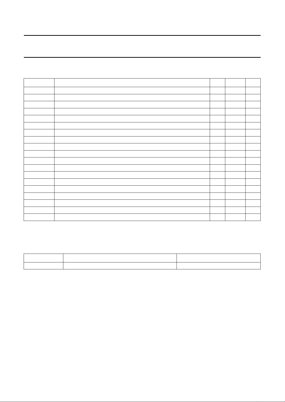
SYMBOL PARAMETER MIN. TYP. MAX. UNIT
V
I
P
V
V
V
V
P
8(p-p)
6(p-p)
7(p-p)
14
supply voltage (pin 5) 7.2 8.0 8.8 V
supply current (pin 5) 80 100 120 mA
luminance input (peak-to-peak value) (C)VBS − 0.45/ 1.43 − V
−(B−Y) input (peak-to-peak value) − 1.33 − V
−(R−Y) input (peak-to-peak value) − 1.05 − V
three-level sandcastle pulse
H+V − 2.5 − V
H − 4.5 − V
BK − 8.0 − V
two-level sandcastle pulse
H+V − 2.5 − V
BK − 4.5 − V
V
i
V
O(p-p)
T
amb
RGB input signals at pins 2, 3, 4, 10, 11 and 12 (black-to-white value) − 0.7 − V
RGB output at pins 24, 22 and 20 (black-to-white value) − 2.0 − V
operating ambient temperature −20 −+70 °C
May 1994 2
Page 3

Philips Semiconductors Preliminary specification
RGB video processor with automatic
cut-off control and gamma adjust
ORDERING INFORMATION
EXTENDED
TYPE NUMBER
TDA4780 28 DIL plastic SOT117
Note
1. SOT117-1; 1996 December 9.
PINS
POSITION
PIN
TDA4780
PACKAGE
MATERIAL CODE
(1)
May 1994 3
Page 4
Philips Semiconductors Preliminary specification
RGB video processor with automatic
cut-off control and gamma adjust
TDA4780
Fig.1 Block diagram (continued in Fig.2)
May 1994 4
Page 5
Philips Semiconductors Preliminary specification
RGB video processor with automatic
cut-off control and gamma adjust
TDA4780
Fig.2 Block diagram (continued from Fig.1)
May 1994 5
Page 6
Philips Semiconductors Preliminary specification
RGB video processor with automatic
cut-off control and gamma adjust
PINNING
SYMBOL PIN DESCRIPTION
FSW
2
R
2
G
2
B
2
V
P
−(B−Y) 6 colour difference input −(B−Y)
−(R−Y) 7 colour difference input −(R−Y)
Y 8 luminance input
GND 9 ground
R
1
G
1
B
1
FSW
1
SC 14 sandcastle pulse input
BCL 15 average beam current limiting
C
PDL
C
L
C
PDST
CI 19 cut-off measurement input
B
O
C
B
G
O
C
G
R
O
C
R
YHUE 26 Y-output/hue adjust output
SDA 27 I
SCL 28 I
1 fast switch 2 input
2 red input 2
3 green input 2
4 blue input 2
5 supply voltage
10 red input 1
11 green input 1
12 blue input 1
13 fast switch 1 input
input
16 storage capacitor for peak
limiting
17 storage capacitor for leakage
current compensation
18 storage capacitor for peak dark
20 blue output
21 blue cut-off storage capacitor
22 green output
23 green cut-off storage capacitor
24 red output
25 red cut-off storage capacitor
2
C-bus serial data
input/acknowledge output
2
C-bus serial clock input
TDA4780
Fig.3 Pin configuration.
May 1994 6
Page 7

Philips Semiconductors Preliminary specification
RGB video processor with automatic
cut-off control and gamma adjust
GENERAL DESCRIPTION
(continued)
The required input signals are:
• luminance and negative colour difference signals
• 2- or 3-level sandcastle pulse for internal timing pulse
generation
• I2C-bus data and clock signals
Two sets of analog RGB colour signals can also be
inserted, e.g. one from a peritelevision connector (SCART
plug) and the other one from an on-screen display (OSD)
generator. The TDA4780 has I2C-bus control of all
parameters and functions with automatic cut-off control of
the picture tube cathode currents. It provides RGB output
signals for the video output stages. In clamped output
mode it can also be used as an RGB source.
The main differences to the sister type TDA4680 are:
• additional features, namely gamma adjust, adaptive
black, blue stretch and two different peak drive limiters.
• the measurement lines are triggered by the trailing edge
of the vertical component of the sandcastle pulse.
• I2C-bus receiver only. Automatic white level control is
not provided; the white levels are determined directly by
the I2C-bus data.
• the TDA4780 is pin compatible (except pin 18) to the
TDA4680. The slave address via the I2C-bus can be
used for both ICs; where a function is not included in the
TDA4680 then the I2C-bus command is not executed.
Special commands (except control bit FSWL) for the
TDA4680 will be ignored by the TDA4780.
TDA4780
FUNCTIONAL DESCRIPTION
Signal input stages
The TDA4780 contains 3 sets of input signal stages for:
a) Luminance/colour-difference signals: (Y: 0.45 V(p-p)
VBS or 1.43 V(p-p) VBS, selectable via I
1.05 V(p-p); −(B−Y): 1.33 V(p-p)). The capacitively
coupled signals are matrixed to RGB signals by either a
PAL/SECAM or NTSC matrix (selected via I2C-bus).
b) (RGB)1signals (0.7 V(p-p) VB), capacitively coupled
(e.g. from external source).
c) (RGB)2signals (0.7 V(p-p) VB), capacitively coupled
(e.g. videotext, OSD).
All input signals are clamped in order to have the same
black levels at the signal switch input. Displayed signals
must be synchronous with the sandcastle pulse.
Signal switches
Both fast signal switches can be operated by switching
pins (e.g. SCART facilities) or set via the I
switch 1 the Y-CD signals or the (RGB)1signals can be
selected, by switch 2 the above selected signals or the
(RGB)2signals are enabled. During the vertical and
horizontal blanking time an artificial black level equal to the
clamped black level is inserted in order to clip off the sync
pulse of the luminance signal and to suppress hum during
the cut-off measurement time and eliminate noise during
these intervals.
Saturation, gamma, contrast and brightness adjust
Saturation, contrast and brightness adjusts are adjusted
via the I
signals. Gamma acts on the luminance content of the input
signals.
2
C-bus and act on Y, CD as well as on RGB input
2
C-bus, −(R−Y):
2
C-bus. By
May 1994 7
Gamma adjust
The gamma adjust stage has a non-linear transmission
characteristic according to the formula y = x
represents the input and y the output signal. If gamma is
smaller than unity, the lower parts of the signal are
amplified with higher gain.
Adaptive black (ADBL)
The adaptive black stage detects the lowest voltage of the
luminance component of the internal RGB signals during
the scanning time and shifts it to the nominal black level.
In order to keep the nominal white level the contrast is
increased simultaneously.
gamma
, where x
Page 8

Philips Semiconductors Preliminary specification
RGB video processor with automatic
cut-off control and gamma adjust
Blue stretch (BLST)
The blue stretch channel gets additional amplification if the
blue signal is greater than 80% of the nominal signal
amplitude. In that case the white point is shifted towards
higher colour temperature so that white parts of a picture
seem to be brighter.
Measurement pulse and blanking stage
During the vertical and horizontal blanking time and the
measurement period the signals are blanked to an ultra
black level, so the leakage current of the picture tube can
be measured and automatically compensated for.
During the cut-off measurement lines (one line period for
each R, G or B) the output signal levels are at cut-off
measurement level.
The vertical blanking period is timed by the sandcastle
pulse. The measurement pulses (leakage, R, G and B) are
triggered by the negative going edge of the vertical pulse
of the sandcastle pulse and start after the following
horizontal pulse.
The IC is prepared for 2f
Output amplifier and white adjust potentiometer
(32 kHz) application.
H
TDA4780
limiting, that is activated if one of the RGB signals even
shortly exceeds a via I2C-bus adjusted threshold. The
latter can be either referred to the cut-off measurement
level of the outputs or to ground.
When signal limiting occurs, contrast is reduced, and at
minimum contrast brightness is reduced additionally.
Sandcastle decoder and timer
A 3-level detector separates the sandcastle pulse into
combined line and field pulses, line pulses, and clamping
pulses. The timer contains a line counter and controls the
cut-off control measurement. Application with a 2-level 5 V
sandcastle pulse is possible.
Switch on delay circuit
After switch on all signals are blanked and a warm up test
pulse is fed to the outputs during the cut-off measurement
lines. If the voltage at the cut-off measurement input
exceeds an internal level the cut-off control is enabled but
the signal remains still blanked. The signal blanking is
finished when the cut-off control has stabilized. In case of
output clamping, the cut-off control is disabled and the
switch on procedure will be skipped.
The RGB signals are amplified to nominal 2 V(p-p), the
DC-levels are shifted according to cut-off control.
The nominal signal amplitude can be varied by ±50% by
the white point adjustment via the I
RGB respect).
Automatic cut-off control
During leakage measurement time the leakage current is
compensated in order to get a reference voltage at the
cut-off measurement info pin.
This compensation value is stored in an external capacitor.
During cut-off current measurement times for the R, G and
B channels, the voltage at this pin is compared with the
reference voltage, which is individually adjustable via
2
C-bus for each colour channel. The so derived control
I
voltages are stored in the external feedback capacitors.
Shift stages add these voltages to the corresponding
output signals.
The automatic cut-off control may be disabled via the
I2C-bus. In this mode the output voltage is clamped to
2.5 V. Clamping periods are the same as the cut-off
measurement periods.
Signal limiting
2
C-bus (individually for
Y output and hue adjust
The TDA4780 contains a D/A converter for hue adjust. The
analog information can be fed, e.g. to the multistandard
decoder TDA4650 or TDA4655. This output pin may be
switched to a Y output signal, which can be used for scan
velocity modulation (SCAVEM). The Y output is the Y input
signal or the matrixed (RGB) input signal according to the
switch position of fast switch.
2
C-bus
I
The TDA4780 contains an I2C-bus receiver for control
function.
ESD protection
Pins are provided with protection diodes against ground
and supply voltage (see pin description).
2
C-bus input pins do not shunt the I2C-bus signals in case
I
of missing supply voltage.
EMC
Pins are protected against electromagnetic radiation.
The TDA4780 provides two kinds of signal limiting. First,
an average beam limiting, that reduces signal level if a
certain average is exceeded. Second, a peak drive
May 1994 8
Page 9
Philips Semiconductors Preliminary specification
RGB video processor with automatic
TDA4780
cut-off control and gamma adjust
LIMITING VALUES
In accordance with the Absolute Maximum Rating System (IEC 134).
SYMBOL PARAMETER MIN. MAX. UNIT
T
stg
T
amb
P
tot
= V
V
5-9
P
V
10,11,12-9
V
2,3,4-9
V
8,7,6-9
V
13,1-9
V
25,23,21,17-9
V
14-9
V
15-9
V
16-9
V
27,28-9
I
26
V
18-9
V
19-9
I
24,22,20
I
24,22,20
ESD electrostatic handling (note 1) for all pins −500 +500 V
storage temperature −20 +150 °C
operating ambient temperature −20 +70 °C
total power dissipation − 1200 mW
supply voltage −0.1 +9.0 V
(RGB)1inputs −0.1 V
(RGB)2inputs −0.1 V
Y, CD-inputs −0.1 V
switch I, II −0.1 V
black level, leakage storage −0.1 V
P
P
P
P
P
sandcastle −0.7 VP+ 5.8 V
average current inf. −0.7 VP+ 0.7 V
peak drive storage −0.1 V
I2C-bus −0.1 V
P
P
Y output / hue adjust −8 − mA
peak dark storage −0.1 V
P
cut-off control input −0.7 VP+ 0.7 V
output peak −20 − mA
output average −10 − mA
V
V
V
V
V
V
V
V
Note to the Limiting Values
1. Charge device model class A: discharging a 200 pF capacitor through a 0 Ω series resistor.
THERMAL RESISTANCE
SYMBOL PARAMETER THERMAL RESISTANCE
R
th j-a
from junction to ambient in free air 47 K/W
QUALITY SPECIFICATION
URV-4-2-59/601
May 1994 9
Page 10
Philips Semiconductors Preliminary specification
RGB video processor with automatic
TDA4780
cut-off control and gamma adjust
CHARACTERISTICS
= +25 °C; VP= 8 V; V
T
amb
gamma = 1; adaptive black inactive; brightness, contrast, saturation and white balance at nominal settings; no beam
current or peak drive limiting; all voltages are related to ground (pin 9) and measured in Figs 1 and 2; unless otherwise
specified.
SYMBOL PARAMETER CONDITIONS MIN. TYP. MAX. UNIT
V
P
I
P
supply voltage (pin 5) 7.2 8 8.8 V
supply current (pin 5) − 100 120 mA
Colour-difference inputs (−(B−Y): pin 6, −(R−Y): pin 7; capacitively coupled to a low ohmic source;
recommendation: maximum 600 Ω)
V
6
−(B−Y) signal (peak-to-peak
value)
V
6,7
I
6,7
internal bias during clamping − 4.0 − V
DC input current between
clamping pulses
I
6,7
maximum input current during
clamping
V
7
−(R−Y) signal (peak-to-peak
value)
R
6,7
AC input resistance 10.0 −− MΩ
Y input (pin 8; capacitively coupled to a low ohmic source; recommendation: maximum 600 Ω)
V
8
input signal (composite signal;
VBS; peak-to-peak value)
R
8
V
8
I
8
AC input resistance 10.0 −− MΩ
internal bias during clamping YHI = 0 − 3.7 − V
DC input current between
clamping pulses
I
8
maximum input current during
clamping
: nominal signal amplitude (black-white) 2000 mV (peak-to-peak value) at output pins;
nom
75% colour bar signal − 1.33 − V
−− 0.1 µA
100 180 260 µA
75% colour bar signal − 1.05 − V
adaption to two different signal
levels via control bit YHI
YHI = 0 − 0.45 − V
YHI = 1 − 1.43 − V
YHI = 1 − 4.6 − V
−− 0.1 µA
100 180 260 µA
RGB input 1 (R
: pin 10, G1: pin 11, B1: pin 12; capacitively coupled to a low ohmic source;
1
recommendation: maximum 600 Ω; note 1)
V
10,11,12
R
10,11,12
V
10,11,12
I
10,11,12
input signal (peak-to-peak value) − 0.7 − V
AC input resistance 10.0 −− MΩ
internal bias during clamping − 5.1 − V
DC input current between
clamping pulses
I
10,11,12
maximum input current during
clamping
May 1994 10
−− 0.1 µA
100 180 260 µA
Page 11
Philips Semiconductors Preliminary specification
RGB video processor with automatic
TDA4780
cut-off control and gamma adjust
SYMBOL PARAMETER CONDITIONS MIN. TYP. MAX. UNIT
RGB input 2 (R2: pin 2, G2: pin 3, B2: pin 4; capacitively coupled to a low ohmic source;
recommendation: maximum 600 Ω; note 1)
V
2,3,4
R
2,3,4
V
2,3,4
I
2,3,4
I
2,3,4
PAL/SECAM and NTSC matrix (note 2; for demodulation axis see appendix)
PAL/SECAM matrix control bit NMEN = 0
NTSC matrix control bit NMEN = 1; hue position set on (−2) degrees
Fast signal switches and blanking (fast signal switch 1 (pin 13); Y, CD / R
V
13
V
13
R
13
Crosstalk (see Table 2)
− t
t
s
i
input signal (peak-to-peak value) − 0.7 − V
AC input resistance 10.0 −− MΩ
internal bias during clamping − 5.1 − V
DC input current between
−− 0.1 µA
clamping pulses
maximum input current during
100 180 260 µA
clamping
, G1; B1; control bits FSDIS1, FSON1)
1
voltage to select Y and CD − 0 0.4 V
voltage range to select R1, G
and B
1
1
0.9 1.0 5.5 V
internal resistor to ground 3.3 3.8 4.8 kΩ
difference between transit times
−− 10 ns
for signal switching and signal
insertion
Fast signal switch 2 (pin 1; Y, CD or R
V
1
V
1
V
1
voltage to select Y and CD /
R1,G1and B
1
voltage range to select R2,
G2and B
2
required minimal voltage to switch
off the ADBL measurement
R
1
internal resistor to ground R1> R
Crosstalk (see Table 2)
− t
t
s
i
difference between transit times
for signal switching and signal
insertion
, G1, B1 / R2,G2,B2; control bits FSDIS2, FSON2)
1
− 0 0.4 V
0.9 1.0 5.5 V
− 0.87 1.0 V
13
2.8 4.2 6.0 kΩ
−− 10 ns
May 1994 11
Page 12

Philips Semiconductors Preliminary specification
RGB video processor with automatic
TDA4780
cut-off control and gamma adjust
SYMBOL PARAMETER CONDITIONS MIN. TYP. MAX. UNIT
Adjust stages (adaptive black, gamma, contrast, saturation, brightness and white point adjust, blue stretch)
Adaptive black (detectors inactive status due to action of fast switch 2 (pin 1); see Table 1, Fig.9 and note 3)
I
18
discharge current of peak dark
storage capacitor
I
18
charge current of peak dark
storage capacitor
maximum level shift: ∆ black level
in percent of nominal signal
amplitude
difference between nominal black
and adaptive black in percent of
nominal signal amplitude
detectors inactive time before
blanking
detectors inactive time after
blanking
Gamma adjust
Acts on internal Y signal; Y matrix see Y output; I
Resolution 6 bit
range of gamma
minimum (3F
maximum (00
) − 0.7 −−
HEX
) − 1.0 −−
HEX
maximum gain at minimum
gamma
Saturation adjust
Acts on RGB signals; Y matrix see Y output; I
Resolution 1.5% of maximum saturation
2
C-bus data for nominal
I
saturation
maximum saturation I
minimum saturation I
outside active
0.1 0.5 1.0 µA
measurement window
inside active
1.5 2.5 3.5 µA
measurement window
−360 −300 −250 µA
10 13 16 %
−30 +3%
2.3 3.1 4.0 µs
2.3 2.5 3.4 µs
2
C-bus controlled potentiometer (subaddress 0B)
near nominal black 5 6 7 dB
2
C-bus controlled potentiometers (subaddress 01)
1F 20 21 HEX
2
C-bus data 3F
HEX;
4.9 5.5 6.1 dB
measured at 100 kHz;
relative to nominal saturation
2
C-bus data 00
HEX;
−− −50 dB
measured at 100 kHz;
relative to typical value of
maximum saturation
May 1994 12
Page 13

Philips Semiconductors Preliminary specification
RGB video processor with automatic
TDA4780
cut-off control and gamma adjust
SYMBOL PARAMETER CONDITIONS MIN. TYP. MAX. UNIT
Contrast adjust
Acts on RGB signals; I2C-bus controlled potentiometers (subaddress 02)
Resolution 1.5% of maximum contrast
2
C-bus data for nominal contrast 20 22 24 HEX
I
2
maximum contrast I
C-bus data 3F
HEX;
limiters inactive;
relative to nominal contrast
2
minimum contrast I
C-bus data 00
HEX;
relative to maximum
Brightness adjust
2
Acts on RGB signals; I
C-bus controlled potentiometers (subaddress 00)
Resolution 1.5% of range; ∆ black level in percent of nominal signal amplitude referred to cut-off measuring level
maximum brightness: ∆ black
3F
HEX
level
nominal brightness: ∆ black level 29
minimum brightness: ∆ black level 00
maximum brightness: ∆ black
level
minimum brightness: ∆ black level 00
HEX
HEX
HEX;
control bits
3F
BCOF = 1 and MOD2 = 0
control bits
HEX;
BCOF = 1 and MOD2 = 0
Blue stretch
2
Blue stretch is activated by I
C-bus control bit BLST = 1 (see Fig.11)
increase of small signal gain 100% of nominal signal
amplitude and at 1 MHz
Differences of black level steps
Differences from channel to channel of the ratio of the difference (black level cut-off measurement level) to actual
nominal signal amplitude (V
nom24,Vnom22,Vnom20
) over the whole contrast, brightness and saturation range, switching
matrix or switching fast switches, gamma = 1, BLST = 0, ADBL = 0
dV/V
static deviation dV/V
nom
dV22/V
dV20/V
dV20/V
nom
nom22
nom20
nom20;
= dV24/V
=dV24/ V
= dV22/V
ripple on pin 5
nom24
−
nom24 −
nom22
during clamping ≤ 1 mV;
note 8
at nominal saturation −0.5 −+0.5 %
− 4.5 5.5 dB
−28 −22 −16 dB
23 30 37 %
−70 +7%
−58 −50 −42 %
23 30 37 %
−58 −50 −42 %
15 20 25 %
−1.0 −+1.0 %
−
May 1994 13
Page 14

Philips Semiconductors Preliminary specification
RGB video processor with automatic
TDA4780
cut-off control and gamma adjust
SYMBOL PARAMETER CONDITIONS MIN. TYP. MAX. UNIT
RGB outputs (output for positive RGB signals (R: pin 24, G: pin 22, B: pin 20); following data without external load)
R
24,22,20
I
24,22,20
V
24,22,20
V
24,22,20
V
24,22,20
V
24,22,20
V
24,22,20
V
24,22,20
Output clamp (RGB)
V
20,22,24
White potentiometers
Overall white point deviation
dV/V
differential output resistance − 25 30 Ω
maximum output current 4.0 5.0 − mA
minimum output voltage note 9 −− 0.8 V
maximum output voltage RL≥ 2 kΩ 6.3 7.0 − V
maximum signal amplitude
3.3 −− V
(black-white) due to internal limits
(peak-to-peak value)
nominal signal amplitude
(black-white; peak-to-peak value)
at nominal white adjust;
contrast and saturation
1.7 2.0 2.3 V
setting; gamma = 1; nominal
input signals
range of cut-off measurement
note 9 1.0 − 5.0 V
level
recommended cut-off
− 3.0 − V
measurement level
clamp voltage black level control bit BCOF = 1 2.3 2.5 2.7 V
2
C-bus data for nominal settings 21 22 23 HEX
I
maximum increase of AC gain 3F
maximum decrease of AC gain 00
nom
dV/V
dV22/V
dV20/V
dV20/V
nom
nom22
nom20
nom20
= dV24/V
= dV24/V
= dV22/V
nom24
nom24
nom22
meaning of actual nominal signal
see ‘differences of black level
step’; over whole contrast range
see ‘contrast adjust’
HEX
HEX
−
−
−
input: (RGB)
1,2
differences from channel to
channel of the ratio of the
difference (signal white level
cut-off measurement level) to
actual nominal signal
amplitude (V
V
nom 20
nom 24, Vnom 22,
) over the whole
40 50 60 %
40 50 60 %
−2.0 −+2.0 %
saturation range at
nominal contrast, brightness
and nominal input signals;
ripple on pin 5 during clamping
≤ 1 mV; note 8
Frequency behaviour, crosstalk
Between the Y input (pin 8) and the RGB outputs (pins 24, 22 and 20)
decrease in gain 1 MΩ and 20 pF load at
−− 3dB
13 MHz
Between the colour-difference inputs (pins 7 and 6) and the corresponding R and B outputs (pins 24 and 20)
decrease in gain at 13 MHz −− 3dB
Between the (RGB)
inputs (pins 10, 11 and 12 or 2, 3 and 4) and the RGB outputs (pins 24, 22 and 20)
1,2
decrease in gain at 22 MHz −− 3dB
May 1994 14
Page 15

Philips Semiconductors Preliminary specification
RGB video processor with automatic
TDA4780
cut-off control and gamma adjust
SYMBOL PARAMETER CONDITIONS MIN. TYP. MAX. UNIT
Sandcastle input (pin 14; control bit SC5; note 4)
I
14
C
14-9
V
14
Clamp pulse delay
Required minimal burst gate pulse width
input current V14< 0.5 V −− −100 µA
input capacitance −− 10 pF
required voltage range
for horizontal and vertical
blanking pulses SC5 = 0 or SC5 = 1 2.0 2.5 3.0 V
for horizontal pulses (line count) SC5 = 0 4.0 4.5 4.9 V
for burst key pulses SC5 = 0 6.1 − V
for burst key pulses and
SC5 = 1 4.0 − V
+ 5.8 V
P
+ 5.8 V
P
line count
delay of leading edge of clamping
pulse
nominal sandcastle pulse
DELOF = 0 1.2 1.5 1.8 µs
DELOF = 1 − 0 −µs
DELOF = 0 line frequency = 16 kHz 3 −− µs
DELOF = 1 line frequency = 32 kHz 1.5 −− µs
Generation of measurement lines and blanking
Blanking to ultra black level occurs during time DG except MR in R-channel, MG in G-channel, MB in B-channel (see
pulse diagram Fig.12)
Difference between ultra black level (VUB) and measurement level (VCL) in percent of nominal signal amplitude
(independent of white point adjust)
dV/V
dV = VCL − VUB no clipping 25 35 45 %
nom
Leakage current measuring time:
LM will start after the end of vertical sandcastle (see pulse diagram)
Vertical blanking period and cut-off measurement lines (see pulse diagram)
The vertical component will be identified if it contains 2 or more burst key pulses in case of SC5 = 1 or two or more
line pulses (H) in case of SC5 = 0
The line counter is triggered by the leading edge
The blanking time is valid for a vertical pulse detected by the sandcastle decoder
The internal blank pulse is OR gated with the sandcastle vertical pulse and the end of the measurement pulses
Insertion time: full line period
Measurement time: line period minus horizontal period (50/60 Hz)
Line sequence of measuring lines:
First line after end of horizontal pulse which followed the end of vertical pulse: leakage measurement LM
First line after leakage pulse: red measurement MR
Second line after leakage pulse: green measurement MG
Third line after leakage pulse: blue measurement MB (see pulse diagram)
May 1994 15
Page 16

Philips Semiconductors Preliminary specification
RGB video processor with automatic
TDA4780
cut-off control and gamma adjust
SYMBOL PARAMETER CONDITIONS MIN. TYP. MAX. UNIT
Warm up test pulse during MT (see pulse diagram)
V
WU
warm up level VWU= VPL− 1 V;
VPL= peak drive level
(see also signal limiting);
given by I2C-bus;
subaddress OA; no warm
up test pulse in case of
output clamping
(BCOF = 1)
maximum warm up level 3F
HEX
Threshold for Power On Reset (POR) during time DG (see pulse diagram)
V
20,22,24
POR
output voltage to cause POR RELC = 0 − V
RELC = 1 − V
Y output (pin 26; note 5)
V
26
nominal signal amplitude
(black-white; independent of
gamma, adaptive black and
control bit YEXH = 1;
hue DAC (register 03)
set > 28
HEX
contrast; peak-to-peak value)
V
R
∆τ
26
26
26
black level YEXH = 1
3F
HEX
20
HEX
Y matrix coefficients Y = a
a
r
a
g
a
b
R+agG+abB
r
differential output resistance − 190 230 Ω
group delay time between RGB outputs and Y
output
f
g
3 dB bandwidth 11 15 − MHz
Automatic cut-off control (pin 19; measurement periods see beam info on pin 19)
V
19
permissible voltage (also during
scanning period)
V
I
19
I
19
R
REF0
19
internally controlled voltage on
pin 19
during leakage measurement
time LM
maximum output current −350 −−250 µA
maximum input current 250 − 350 µA
input resistance for
measurement input
I
19
V
19
additional input current only during warm up − 0.5 − mA
threshold of warm up detector
(active in line MG)
−− − −
5.6 6.0 6.3 V
− V
PL
+1− V
PL
0.85 1.0 1.15 V
− 4.0 − V
− 2.0 − V
0.27 0.30 0.33 −
0.53 0.59 0.65 −
0.10 0.11 0.12 −
20 25 30 ns
−− V
−1.4 V
P
2.4 2.7 3.0 V
1 −− MΩ
4.3 4.5 4.7 V
May 1994 16
Page 17

Philips Semiconductors Preliminary specification
RGB video processor with automatic
TDA4780
cut-off control and gamma adjust
SYMBOL PARAMETER CONDITIONS MIN. TYP. MAX. UNIT
V
MEAS
Storage of cut-off control voltage / output clamping voltage (pins 25, 23 and 21)
I
25,23,21
I
25,23,21
Storage of leakage information (pin 17)
I
17
I
17
I
17
V
17
difference between input voltage
for cut-off and V
REF0;
adjustable
−− − −
via I2C-bus (subaddress for
reference: R: 07, G: 08 and B: 09)
maximum V
nominal V
minimum V
MEAS
MEAS
MEAS
input currents of storage inputs
3F
20
00
HEX
HEX
HEX
1.5 1.6 1.7 V
0.9 1.0 1.1 V
0.4 0.45 0.5 V
−− 0.1 µA
outside of the measurement time
maximum charge / discharge
0.2 0.3 0.4 mA
current during measurement time
amplification from storage pins
− 1.7 −−
25, 23 and 21 to outputs
maximum charge / discharge
300 400 −µA
current at time LM
discharge current peak limiting during time MK
− 4 − mA
active
leakage current outside time LM −− 0.1 µA
voltage to reset IC to switch on
V17is below 2.3 2.5 3.0 V
conditions
Signal limiting (The limitation acts on contrast and at low contrast on brightness)
Average beam current limiting (pin 15)
V
dV
15
15
start of contrast reduction − 4 − V
input range for full contrast
reduction
V
15
dV
15
start of brightness reduction − 2.5 − V
input range for full brightness
reduction
I
15
input current −− −0.5 µA
Peak signal limiting of output signals (pin 16)
The limitation acts 1 H delayed
2
Limiting level adjustable by I
V
24,22,20
V
24,22,20
I
16
maximum limiting level extrapolated from 2F 6.8 − 7.2 V
minimum limiting level 00
maximum discharge current at
C-bus (subaddress OA; control bit RELC = 0)
HEX
RELC = 0 4 − 6mA
peak drive
−−2 − V
−−1.6 − V
− 2.3 3 V
May 1994 17
Page 18

Philips Semiconductors Preliminary specification
RGB video processor with automatic
TDA4780
cut-off control and gamma adjust
SYMBOL PARAMETER CONDITIONS MIN. TYP. MAX. UNIT
Peak signal limiting (pin 16)
Control bit RELC = 1; Limiting Level (V
V
LiL
maximum limiting level 3F
minimum limiting level 00
Peak drive limiting starts, if the maximum of the RGB signals after white point adjustment exceeds a threshold
Cut-off measurement level MX = MR or MB or MG
Discharge currents
The total discharge current is a summation of I
Threshold 1 (TH1)
I
16(1)
maximum discharge current TH1 = MX + V
steepness − 1.5 − mA / 0.1 V
Low-pass filter, control bit TCPL
t
DPDL
t
DPDL
time constant low-pass filter TCPL = 1 (at 1fH); RELC = 1 0.9 1.2 1.5 µs
time constant low-pass filter TCPL = 0 (at 2fH); RELC = 1 0.4 0.6 0.8 µs
Threshold 2 (TH2)
I
16(2)
maximum discharge current TH2 = MX + V
steepness − 1.5 − mA / 0.1 V
Threshold 3 (TH3)
I
16(3)
maximum discharge current TH3 = MX + V
steepness − 0.15 − mA / 0.1 V
Charge current
I
16
V
dV
16
16
charge current −0.5 −1 −2 µA
start of contrast reduction − 4 − V
input range for full contrast
reduction
V
16
dV
16
start of brightness reduction − 2.5 − V
input range for full brightness
reduction
V
16
maximum voltage by internal
limitation
) adjustable by I2C-bus (subaddress OA)
LiL
equal gain in white point
adjust; signal only in one
output channel
HEX
HEX
+ I
16(1)
16(2)
+ I
16(3)
LiL
; 1 line
delayed and low-pass filtered
× 1.10; 1 line
LiL
delayed
; undelayed 0.45 0.6 0.75 mA
LiL
3.3 3.5 3.9 V
1.3 1.5 1.7 V
4.5 6 7.5 mA
4.5 6 7.5 mA
−−2 − V
−−1.6 − V
4.5 −− V
Hue adjust output (pin 26; note 6)
V
26
V
26
V
26
I
26
minimum output voltage YEXH = 0; 00
nominal output voltage YEXH = 0; 20
maximum output voltage YEXH = 0; 3F
current of internal emitter follower 500 700 −µA
May 1994 18
HEX
HEX
HEX
0.5 − 1.0 V
3.0 3.2 3.4 V
4.8 − 5.5 V
Page 19

Philips Semiconductors Preliminary specification
RGB video processor with automatic
TDA4780
cut-off control and gamma adjust
SYMBOL PARAMETER CONDITIONS MIN. TYP. MAX. UNIT
I2C-bus inputs
f
28
t
SU;DAT
t
H
t
L
t
r
t
f
Input levels
V
27
V
28
V
27
V
28
I
27
I
28
I
27
I
28
V
27
I
27
clock frequency range 0 − 100 kHz
data set-up 250 −− ns
clock pulse HIGH 4 −− µs
clock pulse LOW 4.7 −− µs
rise time −− 1 µs
fall time −− 0.3 µs
LOW level input voltage −− 1.5 V
−− 1.5 V
HIGH level input voltage 3.0 − 5.5 V
3.0 − 5.5 V
input current V27= 0.4 V −10 −− µA
V28= 0.4 V −10 −− µA
input current V27= 0.9 V −− 10 µA
V28= 0.9 V −− 10 µA
LOW level output voltage −− 0.4 V
output current V27 = 0.4 V 3.0 −− mA
May 1994 19
Page 20

Philips Semiconductors Preliminary specification
RGB video processor with automatic
TDA4780
cut-off control and gamma adjust
Notes to the characteristics
1. RGB signals controlled by saturation, adaptive black, contrast and brightness, gamma affects the Y component of
the internal RGB signals.
2. Matrix coefficients should be tested by comparing RGB output signals with a reference RGB colour bar, which is fed
in at (RGB)1or (RGB)2inputs. In case of NMEN = 1 (NTSC) at minimum saturation the Y output and RGB output
signals are not identical to the Y input signal. PAL/SECAM signals are matrixed by the equation:
V
= −0.51V
G−Y
NTSC signals are matrixed by the equations (hue phase shift of −2 degrees):
V
* = 1.39V
R−Y
In the matrix equations: V
demodulator. V
3. Adaptive black control acts on Y signal, which is either Y input or Y output from RGB matrix. Negative set-up is not
affected. The level shift value is determined by the peak dark detector, operation selected by control bit ADBL. The
peak dark detector is inactive during blanking. Peak dark detector activated by internal line counter, which starts after
the end of the vertical blank of the sandcastle. Active from line 16 (after end of vertical sandcastle) to line 224 (NTSC
mode, NMEN = 1) or line 272 (PAL mode, NMEN = 0). It is recommended to increase the contrast value
(subaddress 02) by 15% if ADBL = 1. The line numbers are doubled if control bit HDTV = 1.
4. Sandcastle pulse detector (pin 14)
The sandcastle pulse is compared with 3 (control bit SC5 = 0) or 2 (SC5 = 1) internal threshold levels to separate the
various pulses; the internal pulses are generated while the input pulse is higher than the thresholds. The thresholds
are independent of supply voltage and temperature.
5. Y output can be switched to hue adjust output via I2C-bus control bit YEXH. Output without sync pulse.
Recommendation: Hue adjust DAC set to 3F
6. Output can be switched to Y output via I2C-bus control bit YEXH (via I2C-bus, resolution 6 bit, bus subaddress 03).
7. At minimum gamma (3F
8. Series resistor in supply voltage should be less than 0.3 Ω.
9. At 1.0 V cut-off measurement level the function of the cut-off control loop is not guaranteed because the blanking
level is limited to the minimum output voltage. For proper working a guide number for the minimum cut-off
measurement level is 1.3 V.
R−Y
R−Y
R−Y
− 0.19V
− 0.07V
*, V
G−Y
B−Y
and V
*=−0.46V
are conventional PAL demodulation axes and amplitudes at the output of the
B−Y
* are the NTSC-modified colour-difference signals.
B−Y
B−Y;VG−Y
R−Y
* and V
) any differences in black level steps are amplified by 6 dB.
HEX
− 0.15V
R−Y
. Black level adjustable via hue adjust DAC.
HEX
B−Y
; V
B−Y
*= V
B−Y
May 1994 20
Page 21

Philips Semiconductors Preliminary specification
RGB video processor with automatic
cut-off control and gamma adjust
APPENDIX
TDA4780
Fig.4 Demodulation axes.
May 1994 21
Page 22

Philips Semiconductors Preliminary specification
RGB video processor with automatic
TDA4780
cut-off control and gamma adjust
I2C-BUS RECEIVER (pins 27 and 28)
S: start condition
P: stop condition
W: write
A: acknowledge
slave address:
A6 A5 A4 A3 A2 A1 A0
10001000
receiver (write mode)
slave receiver format is (BREN = 0)
S SLAVE ADDRESS A SUBADDRESS A DATA BYTE A ... DATA BYTE A P
n data bytes with auto-increment of subaddresses
All subaddresses within the range 00 to 0F are automatically incremented. The subaddress counter wraps around from
0F to 00. Only in this case 0F will be acknowledged too.
Subaddresses outside the range 00 to 0E are not acknowledged by the device and neither auto-increment nor any other
internal operation takes place.
All eight bits of the subaddress have to be decoded by the device.
If BREN = 1 (control register 1) auto-increment is not possible, the slave receiver format is:
S, SLAVE ADDRESS A, SUB ADDRESS A, DATA BYTE A, P
W
:
May 1994 22
Page 23

Philips Semiconductors Preliminary specification
RGB video processor with automatic
TDA4780
cut-off control and gamma adjust
Table 1 Signal input selection and effect on adaptive black measurements by fast source switches and I2C-bus.
2
C-BUS CONTROLLED BITS ANALOG
I
SWITCH
FSON2 FSDIS2 FSON1 FSDIS1
FSW2
(pin 1)
FSW1
(pin 13)
RGB2 (pins 2, 3
and 4)
LLLLLL active ON
L H active ON
H * ON off
LLLHL* active ON
H * ON off
L L H * L * active ON
H * ON off
L H L L * L active ON
* H active ON
L H L H * * active ON
L H H * * * active ON
H L * * L * ON active
HONoff
HH****ON active
SELECTED SIGNALS
ADBL
RGB1(pins
10, 11 and 12
TV (pins
6, 7 and 8)
Notes
1. H: logical HIGH or analog switch (pins 1 and 13) to > 0.9 V
2. L: logical LOW or analog switch (pins 1 and 13) to < 0.4 V
3. *: H or L, no influence
4. ON: is the selected signal input
Table 2 Crosstalk
FSW1 FSW2 CROSSTALK at 4 MHz
maximum value (dB)
L L RGB
L H Y, CD → RGB
L H Y, CD → RGB
H H Y, CD → RGB
→ Y, CD −58 −55 −50
1
→ Y, CD −58 −55 −50
RGB
2
−51 −50 −47
1
RGB
RGB
RGB
→ RGB
2
→ RGB
1
→ RGB
1
−58 −55 −50
1
−51 −50 −47
2
−58 −55 −50
2
−51 −50 −47
2
−58 −55 −50
2
at 8 MHz
maximum value (dB)
at 13 MHz
maximum value (dB)
May 1994 23
Page 24

Philips Semiconductors Preliminary specification
RGB video processor with automatic
TDA4780
cut-off control and gamma adjust
Table 3 Subaddress byte and data byte format.
FUNCTION SUBADDRESS DATA BYTE
D7 D6 D5 D4 D3 D2 D1 D0
brightness 00 0 0 A05 A04 A03 A02 A01 A00
saturation 01 0 0 A15 A14 A13 A12 A11 A10
contrast 02 0 0 A25 A24 A23 A22 A21 A20
hue 03 0 0 A35 A34 A33 A32 A31 A30
red gain 04 0 0 A45 A44 A43 A42 A41 A40
green gain 05 0 0 A55 A54 A53 A52 A51 A50
blue gain 06 0 0 A65 A64 A63 A62 A61 A60
red level reference 07 0 0 A75 A74 A73 A72 A71 A70
green level reference 08 0 0 A85 A84 A83 A82 A81 A80
blue level reference 09 0 0 A95 A94 A93 A92 A91 A90
peak drive limit 0A 0 0 AA5 AA4 AA3 AA2 AA1 AA0
gamma 0B 0 0 AB5 AB4 AB3 AB2 AB1 AB0
control register 1 0C SC5 DELOF BREN X NMEN X X X
control register 2 0D X HDTV FSBL BCOF FSDIS2 FSON2 FSDIS1 FSON1
control register 3 0E ADBL YHI MOD2 BLST YEXH RELC TCPL 0
The least significant bit of an analog control alignment register is defined as AX0 (D0).
After power on reset (PONRES) all alignment registers are set to 01.
X means don’t care but for software compatibility with further video ICs with the same slave address, it is recommended
to set all X to 0.
May 1994 24
Page 25

Philips Semiconductors Preliminary specification
RGB video processor with automatic
cut-off control and gamma adjust
Table 4 RGB processor mode bits control register.
SYMBOL PARAMETER CONDITIONS
Control register 1
SC5 sandcastle 5 V 0 = 3-level sandcastle pulse
1 = 2-level sandcastle pulse
DELOF delay of leading edge of
clamping pulse switched off
BREN buffer register enable 0 = new data are executed just after reception
NMEN NTSC - matrix enable 0 = PAL matrix
Control register 2
HDTV HDTV / progressive scan for
ADBL line counter
FSBL full screen black level, e.g. for
optical measurement
BCOF internal black level control off 0 = automatic cut-off control active
FSON2 fast switch 2 on see Table 1
FSDIS1 fast switch 1 disable
FSDIS2 fast switch 2 disable
FSON1 fast switch 1 on
0 = delay
1 = no delay
1 = data are hold in a latch (buffer register) and will be transferred to
their destination register within the next vertical blanking interval; the
device does not acknowledge any new data transfer until the internal
transfer to the destination register has been completed
1 = NTSC matrix
0 = 272 (PAL), 224 (NTSC) lines
1 = 544 (PAL), 448 (NTSC) lines
0 = normal mode
1 = cut-off measurement level during full field brightness, inactive
1 = RGB outputs clamped to fixed DC levels
TDA4780
Control register 3
ADBL adaptive black 0 = off
1 = on
YHI Y high level 0 = input = 0.315 V
1 = input = 1.0 V(
MOD2 modus 2 0 = inactive (BCOF = 0) AND (MOD2 = 1) is senseless; no output
stabilization
1 = output clamp without brightness adjust, brightness remains active
e.g. for blue stretch
BLST blue stretch 0 = off
1 = on
YEXH Y exclusive hue 0 = pin 26 is switched to hue adjust output
1 = pin 26 is switched to Y output
RELC relative to cut-off 0 = peak drive limit to absolute output
1 = peak drive limit relative to cut-off
TCPL time constant peak drive limiter 0 = 2 f
May 1994 25
1 = 1 f
H
H
(black-white)
(p-p)
(black-white)
(p-p)
Page 26

Philips Semiconductors Preliminary specification
RGB video processor with automatic
cut-off control and gamma adjust
handbook, full pagewidth
MSB LSB
01
module address
Fig.5 The module address byte.
TDA4780
00100
ACKX
R/W
MED696
handbook, full pagewidth
handbook, full pagewidth
STOSAD
STOP
condition
MED697
START
condition
MADSTA
data byte
Fig.6 Data transmission without auto-increment (BREN = 0 or 1)
SAD
START
condition
MADSTA
data byte
data bytes
STO
STOP
condition
MED698
Fig.7 Data transmission with auto-increment (BREN = 0).
May 1994 26
Page 27

Philips Semiconductors Preliminary specification
RGB video processor with automatic
cut-off control and gamma adjust
TDA4780
Fig.8 Test and application circuit.
Fig.9 Cut-off measurement pulses
(1) Insert link BR1 if average beam
current limiting is not applied.
may be omitted.
(2) R
18
May 1994 27
Page 28

Philips Semiconductors Preliminary specification
RGB video processor with automatic
cut-off control and gamma adjust
Fig.10 Principle of adaptive black control.
TDA4780
Fig.11 Principle of blue stretch.
May 1994 28
Page 29

Philips Semiconductors Preliminary specification
RGB video processor with automatic
cut-off control and gamma adjust
TDA4780
LM = leakage current measurement time
MR, MG, MB = R, G, B cut-off measurement pulses
Fig.12 Leakage and cut-off current measurement timing diagram.
May 1994 29
Page 30

Philips Semiconductors Preliminary specification
RGB video processor with automatic
cut-off control and gamma adjust
Table 5 internal circuitry (Abbreviations: OB: open base and CL: clamp pulse).
PIN
NO.
1 fast switch 2
2R
PIN NAME
(DESCRIPTION)
input clamp 100 µA / OB
2
WAVE FORM Z INTERNAL CIRCUIT
TDA4780
3G
4B
May 1994 30
input clamp 100 µA / OB
2
input clamp 100 µA / OB
2
Page 31

Philips Semiconductors Preliminary specification
RGB video processor with automatic
cut-off control and gamma adjust
PIN
NO.
5 supply voltage
6 −(B−Y) input clamp 100 µA / OB
PIN NAME
(DESCRIPTION)
WAVE FORM Z INTERNAL CIRCUIT
TDA4780
7 −(R−Y) input clamp 100 µA / OB
8 Y input clamp 100 µA / OB
May 1994 31
Page 32

Philips Semiconductors Preliminary specification
RGB video processor with automatic
cut-off control and gamma adjust
PIN
NO.
9 ground
10 R
PIN NAME
(DESCRIPTION)
input clamp 100 µA / OB
1
WAVE FORM Z INTERNAL CIRCUIT
TDA4780
11 G
12 B
May 1994 32
input clamp 100 µA / OB
1
input clamp 100 µA / OB
1
Page 33

Philips Semiconductors Preliminary specification
RGB video processor with automatic
cut-off control and gamma adjust
PIN
NO.
13 fast switch 1
PIN NAME
(DESCRIPTION)
WAVE FORM Z INTERNAL CIRCUIT
TDA4780
37 kΩ
(SC5 = 0)
14 sandcastle input
15 average beam
current limiting input
storage capacitor
16
for peak limiting
input
OB (SC5 = 1)
OB
outside peak drive OB
during peak drive (RELC = 1) 0 to 12 mA
during peak drive (RELC = 0) 5 mA
May 1994 33
Page 34

Philips Semiconductors Preliminary specification
RGB video processor with automatic
cut-off control and gamma adjust
PIN
NO.
17 storage capacitor
PIN NAME
(DESCRIPTION)
for leakage current
WAVE FORM Z INTERNAL CIRCUIT
outside leakage current
measurement
during leakage current measurement to
automatic switch to power on reset 4 mA
TDA4780
OB
−400 µA
+400 µA
18 peak dark storage OB / 0.26 mA
cut-off −180 µA
19 measurement input
(beam current
information input)
to
+180 µA
May 1994 34
Page 35

Philips Semiconductors Preliminary specification
RGB video processor with automatic
cut-off control and gamma adjust
PIN
NO.
20 blue output
PIN NAME
(DESCRIPTION)
WAVE FORM Z INTERNAL CIRCUIT
TDA4780
5 mA
5 mA
21 blue cut-off storage
capacitor
during cut-off control or during output
clamping
5 mA
OB
−300 µA
to
+300 µA
May 1994 35
Page 36

Philips Semiconductors Preliminary specification
RGB video processor with automatic
cut-off control and gamma adjust
PIN
NO.
22 green output
PIN NAME
(DESCRIPTION)
WAVE FORM Z INTERNAL CIRCUIT
TDA4780
5 mA
5 mA
23 green cut-off
storage capacitor
during cut-off control or during output
clamping
5 mA
OB
−300 µA
to
+300 µA
May 1994 36
Page 37

Philips Semiconductors Preliminary specification
RGB video processor with automatic
cut-off control and gamma adjust
PIN
NO.
24 red output
PIN NAME
(DESCRIPTION)
WAVE FORM Z INTERNAL CIRCUIT
TDA4780
5 mA
5 mA
25 red cut-off storage
capacitor
Y output 0.7 mA
26
during cut-off control or during output
clamping
5 mA
OB
−300 µA
to
+300 µA
hue adjust output YEXH = 0
DC 0.8 V to 5.0 V 0.7 mA
May 1994 37
Page 38

Philips Semiconductors Preliminary specification
RGB video processor with automatic
cut-off control and gamma adjust
PIN
NO.
27
PIN NAME
(DESCRIPTION)
I2C-bus data input outside acknowledge OB
acknowledge output during acknowledge
WAVE FORM Z INTERNAL CIRCUIT
TDA4780
less than
0.1 V up
to 4 mA
due to
external
pull-up
resistor
28 I
2
C-bus serial clock
input
OB
May 1994 38
Page 39

Philips Semiconductors Preliminary specification
RGB video processor with automatic
cut-off control and gamma adjust
PACKAGE OUTLINE
handbook, full pagewidth
DIP28: plastic dual in-line package; 28 leads (600 mil)
D
seating plane
L
Z
28
e
b
TDA4780
SOT117-1
M
E
A
2
A
A
1
w M
b
1
15
c
(e )
1
M
H
pin 1 index
1
0 5 10 mm
scale
DIMENSIONS (inch dimensions are derived from the original mm dimensions)
A
A
A
UNIT
inches
Note
1. Plastic or metal protrusions of 0.25 mm maximum per side are not included.
max.
mm
1 2
min.
max.
b
1.7
1.3
0.066
0.051
b
0.53
0.38
0.020
0.014
cD E weM
1
0.32
0.23
0.013
0.009
(1) (1)
36.0
35.0
1.41
1.34
14.1
13.7
0.56
0.54
E
14
(1)
L
3.9
3.4
M
15.80
15.24
0.62
0.60
H
E
17.15
15.90
0.68
0.63
0.252.54 15.24
0.010.10 0.60
e
1
0.15
0.13
Z
max.
1.75.1 0.51 4.0
0.0670.20 0.020 0.16
OUTLINE
VERSION
SOT117-1
IEC JEDEC EIAJ
051G05 MO-015AH
REFERENCES
May 1994 39
EUROPEAN
PROJECTION
ISSUE DATE
92-11-17
95-01-14
Page 40

Philips Semiconductors Preliminary specification
RGB video processor with automatic
cut-off control and gamma adjust
SOLDERING
Introduction
There is no soldering method that is ideal for all IC
packages. Wave soldering is often preferred when
through-hole and surface mounted components are mixed
on one printed-circuit board. However, wave soldering is
not always suitable for surface mounted ICs, or for
printed-circuits with high population densities. In these
situations reflow soldering is often used.
This text gives a very brief insight to a complex technology.
A more in-depth account of soldering ICs can be found in
“IC Package Databook”
our
Soldering by dipping or by wave
The maximum permissible temperature of the solder is
260 °C; solder at this temperature must not be in contact
DEFINITIONS
(order code 9398 652 90011).
TDA4780
with the joint for more than 5 seconds. The total contact
time of successive solder waves must not exceed
5 seconds.
The device may be mounted up to the seating plane, but
the temperature of the plastic body must not exceed the
specified maximum storage temperature (T
printed-circuit board has been pre-heated, forced cooling
may be necessary immediately after soldering to keep the
temperature within the permissible limit.
Repairing soldered joints
Apply a low voltage soldering iron (less than 24 V) to the
lead(s) of the package, below the seating plane or not
more than 2 mm above it. If the temperature of the
soldering iron bit is less than 300 °C it may remain in
contact for up to 10 seconds. If the bit temperature is
between 300 and 400 °C, contact may be up to 5 seconds.
stg max
). If the
Data sheet status
Objective specification This data sheet contains target or goal specifications for product development.
Preliminary specification This data sheet contains preliminary data; supplementary data may be published later.
Product specification This data sheet contains final product specifications.
Limiting values
Limiting values given are in accordance with the Absolute Maximum Rating System (IEC 134). Stress above one or
more of the limiting values may cause permanent damage to the device. These are stress ratings only and operation
of the device at these or at any other conditions above those given in the Characteristics sections of the specification
is not implied. Exposure to limiting values for extended periods may affect device reliability.
Application information
Where application information is given, it is advisory and does not form part of the specification.
LIFE SUPPORT APPLICATIONS
These products are not designed for use in life support appliances, devices, or systems where malfunction of these
products can reasonably be expected to result in personal injury. Philips customers using or selling these products for
use in such applications do so at their own risk and agree to fully indemnify Philips for any damages resulting from such
improper use or sale.
2
PURCHASE OF PHILIPS I
C COMPONENTS
2
Purchase of Philips I
components in the I2C system provided the system conforms to the I2C specification defined by
Philips. This specification can be ordered using the code 9398 393 40011.
May 1994 40
C components conveys a license under the Philips’ I2C patent to use the
 Loading...