

Page 1

INTEGRATED CIRCUITS
DATA SH EET
TDA4685
Video processor with automatic
cut-off control
Preliminary specification
File under Integrated Circuits, IC02
May 1993
Page 2

Philips Semiconductors Preliminary specification
Video processor with automatic cut-off
control
FEATURES
• Operates from an 8 V DC supply
• Black level clamping of the colour difference, luminance
and RGB input signals with coupling-capacitor DC level
storage
• Two analog RGB inputs, selected either by fast switch
signals or the I2C-bus; brightness and contrast control of
these RGB inputs
• Saturation, contrast, brightness and white adjustment
via I2C-bus
• Same RGB output black levels for Y/CD and RGB input
signals
• Timing pulse generation from either a 2- or 3-level
sandcastle pulse for clamping, vertical synchronization
and cut-off timing pulses
• Automatic cut-off control or clamped output selectable
via I2C-bus
• Automatic cut-off control with picture tube leakage
current compensation
• Cut-off measurement pulses after end of the vertical
blanking pulse or end of an extra vertical flyback pulse
• Two switch-on delays to prevent discolouration before
steady-state operation
• Average beam current and peak drive limiting
• PAL/SECAM or NTSC matrix selection via I2C-bus
• Emitter-follower RGB output stages to drive the video
output stages
• I2C-bus controlled DC output e. g. for hue-adjust of
NTSC (multistandard) decoders
GENERAL DESCRIPTION
The TDA4685 is a monolithic, integrated circuit with a
luminance and a colour difference interface for video
processing in TV receivers.
Its primary function is to process the luminance and colour
difference signals from a colour decoder which is equipped
e. g. with the multistandard decoder TDA4655 or TDA9160
plus delayline TDA4661 and the Picture Signal
TDA4685
Improvement (PSI) IC TDA467X or from a Feature
Module. The required input signals are:
• luminance and negative colour difference signals
• 2- or 3-level sandcastle pulse for internal timing pulse
generation
2
C-bus data and clock signals for microprocessor
• I
control.
Two sets of analog RGB colour signals can also be
inserted, e.g. one from a peritelevision connector and the
other from an on-screen display generator. The TDA4685
has I2C-bus control of all parameters and functions with
automatic cut-off control of the picture tube cathode
currents. It provides RGB output signals for the video
output stages.
The TDA4685 is a simplified, pin compatible (except pin
18) version of the TDA4680. The module address via the
I2C-bus can be used for both ICs; where a function is not
included in the TDA4685 then the I2C-bus command is not
executed. The differences with the TDA4680 are:
• no automatic white level control; the white levels are
determined directly by the I2C-bus data
• RGB reference levels for automatic cut-off control are
not adjustable via I2C-bus
• clamping delay is fixed
• only contrast and brightness adjust for the RGB input
signals
• the measurement lines are triggered either by the
trailing edge of the vertical component of the sandcastle
pulse or by the trailing edge of an optional external
vertical flyback pulse (on pin 18), according to which
occurs first.
The TDA4686 is like TDA4685 but intended for double line
frequency application.
May 1993 2
Page 3

Philips Semiconductors Preliminary specification
Video processor with automatic cut-off
TDA4685
control
QUICK REFERENCE DATA
SYMBOL PARAMETER MIN. TYP. MAX. UNIT
V
I
P
V
V
V
V
V
V
T
P
8(p-p)
6(p-p)
7(p-p)
14
i
o(p-p)
amb
supply voltage (pin 5) 7.2 8.0 8.8 V
supply current (pin 5) − 60 − mA
luminance input (peak-to-peak value) − 0.45 − V
−(B−Y) input (peak-to-peak value) − 1.33 − V
−(R−Y) input (peak-to-peak value) − 1.05 − V
three-level sandcastle pulse
H+V − 2.5 − V
H − 4.5 − V
BK − 8.0 − V
two-level sandcastle pulse
H + V − 2.5 − V
BK − 4.5 − V
RGB input signals at pins 2, 3, 4, 10, 11 and 12 (black-to-white value) − 0.7 − V
RGB outputs at pins 24, 22 and 20 (peak-to-peak value) − 2.0 − V
operating ambient temperature 0 − +70 °C
ORDERING INFORMATION
PACKAGE
EXTENDED
TYPE NUMBER
PINS
PIN
POSITION
MATERIAL CODE
TDA4685 28 DIL plastic SOT117
Note
1. SOT117-1; 1996 November 25.
(1)
May 1993 3
Page 4

Philips Semiconductors Preliminary specification
Video processor with automatic cut-off
control
leakage
and cut-off
current input
hue control voltage
26
6-BIT D/A
C
R
cut-off
control
19
CUT-OFF
CONVERTER
leakage
storage
17
COMPARATORS
peak drive
limiting
storage
16
PEAK DRIVE
average
beam
current
15
AND
LIMITING
AVERAGE
BEAM CURRENT
D/A
3 x 6-BIT
CONVERTERS
BCOF
RGB
outputs
O
O
O
B
R
G
242220
OUTPUT
ADJUST,
CUT-OFF
B
R
G
POINT
WHITE
ADJUST
B
R
G
ADJUST,
BLANKING 2,
BRIGHTNESS
MEASUREMENT
B
R
G
STAGES
PULSES
SUPPLY
MED708
21 23 25
9
5
TDA4685
cut-off storage
R
GB
= 8 V
P
V
DELAYS
SWITCH-ON
1ST AND 2ND
A45 to A40, A55 to A50, A65 to A60
AA5 to AA0
C-BUS
2
I
TRANSCEIVER
27
28
SDA
SCL
C-bus
2
I
TDA4685
A05 to A00, A15 to A10, A25 to A20, A35 to A30
BREN
14
18
VFB
sandcastle
TIMING
GENERATOR
BK
(H)
H + V
PULSE
DETECTOR
SANDCASTLE
SC5
pulse
timing
BCOF
FSDIS2, FSON2,
2 x 8-BIT
CONTROL
pulses
FSDIS1, FSON1
NMEN
REGISTERS
13
1
FSW
D/A
4 x 6-BIT
CONVERTERS
101112
1
1
R
G
ADJUST
R
CONTRAST
B
G
handbook, full pagewidth
Fig.1 Block diagram.
BLANKING 1
FAST SIGNAL
SOURCE SWITCH,
B
R
G
NTSC
MATRIX
PAL/SECAM,
C-bus data and
2
control signals
I
ADJUST
SATURATION
8
7
6
1
B
Y
−(R−Y)
−(B−Y)
1
2
FSW
2
3
4
2
2
2
B
R
G
May 1993 4
Page 5

Philips Semiconductors Preliminary specification
Video processor with automatic cut-off
control
PINNING
SYMBOL PIN DESCRIPTION
FSW
2
R
2
G
2
B
2
V
P
−(B−Y) 6 colour difference input −(B−Y)
−(R−Y) 7 colour difference input −(R−Y)
Y 8 luminance input
GND 9 ground
R
1
G
1
B
1
FSW
1
SC 14 sandcastle pulse input
BCL 15 average beam current limiting input
C
PDL
C
L
V
FB
CI 19 cut-off measurement input
B
O
C
B
G
O
C
G
R
O
C
R
HUE 26 hue control output
SDA 27 I
SCL 28 I
1 fast switch 2 input
2 red input 2
3 green input 2
4 blue input 2
5 supply voltage
10 red input 1
11 green input 1
12 blue input 1
13 fast switch 1 input
16 storage capacitor for peak drive limiting
17 storage capacitor for leakage current
18 vertical flyback pulse input
20 blue output
21 blue cut-off storage capacitor
22 green output
23 green cut-off storage capacitor
24 red output
25 red cut-off storage capacitor
2
C-bus serial data input / acknowledge output
2
C-bus serial clock input
lfpage
FSW
1
2
R
2
2
G
3
2
B
4
2
V
5
P
−(B−Y)
6
−(R−Y)
7
Y
8
GND
9
R
10
1
G
11
1
B
12
1
FSW
13
1
SC
14
Fig.2 Pin configuration.
TDA4685
TDA4685
MED709
SCL
28
SDA
27
HUE
26
C
25
R
R
24
O
C
23
G
G
22
O
C
21
B
B
20
O
CI
19
V
18
FB
C
17
L
C
16
PDL
BCL
15
May 1993 5
Page 6

Philips Semiconductors Preliminary specification
Video processor with automatic cut-off
control
I2C-BUS CONTROL
The I2C-bus transmitter provides the
data bytes to select and adjust the
following functions and parameters:
• brightness adjust
• saturation adjust
• contrast adjust
• DC output e. g. for hue control
• RGB gain adjust
• peak drive limiting level adjust
• selects either 3-level or 2-level
(5 V) sandcastle pulse
• enables cut-off control / enables
output clamping
• selects either PAL/SECAM or
NTSC matrix
• enables/disables synchronization
of the execution of I2C-bus
commands with the vertical
blanking interval
• enables Y-CD, RGB1 or RGB2
input.
I2C-BUS TRANSMITTER AND
DATA TRANSFER
2
I
C-bus specification
The I2C-bus is a bi-directional,
two-wire, serial data bus for
intercommunication between ICs in
an equipment. The microcontroller
transmits data to the I2C-bus receiver
in the TDA4685 over the serial data
line SDA (pin 27) synchronized by the
serial clock line SCL (pin 28).
Both lines are normally connected to
a positive voltage supply through
pull-up resistors. Data is transferred
when the SCL line is LOW. When
SCL is HIGH the serial data line SDA
must be stable. A HIGH-to-LOW
transition of the SDA line when SCL is
HIGH is defined as a start bit.
A LOW-to-HIGH transition of the SDA
line when SCL is HIGH is defined as
a stop bit. Each transmission must
start with a start bit and end with a
stop bit. The bus is busy after a start
bit and is only free again after a stop
bit has been transmitted.
TDA4685
2
C-bus receiver
I
(microcontroller write mode)
Each transmission to the I2C-bus
receiver consists of at least three
bytes following the start bit. Each byte
is acknowledged by an acknowledge
bit immediately following each byte.
The first byte is the Module ADdress
(MAD) byte, also called slave address
byte. This includes the module
address, 10001002 for the TDA4685.
The TDA4685 is a slave receiver
(R/W = 0), therefore the module
address byte is 100010002(88 Hex),
see Fig.3.
The length of a data transmission is
unrestricted, but the module address
and the correct sub-address must be
transmitted before the data byte(s).
The order of data transmission is
shown in Fig.4 and Fig.5. Without
auto-increment (BREN = 0 or 1) the
Module ADdress (MAD) byte is
followed by a Sub-ADdress (SAD)
byte and one data byte only (Fig.4).
May 1993 6
Page 7

Philips Semiconductors Preliminary specification
Video processor with automatic cut-off
control
handbook, full pagewidth
MSB LSB
01
module address
Fig.3 The module address byte.
TDA4685
00100
ACK0
R/W
MED710
handbook, full pagewidth
handbook, full pagewidth
STOSAD
STOP
condition
MED697
START
condition
MADSTA
data byte
Fig.4 Data transmission without auto-increment (BREN = 0 or 1).
SAD
START
condition
MADSTA
data byte
data bytes
STO
STOP
condition
MED698
May 1993 7
Fig.5 Data transmission with auto-increment (BREN = 0).
Page 8

Philips Semiconductors Preliminary specification
Video processor with automatic cut-off
control
Auto-increment
The auto-increment format enables
quick slave receiver initialization by
one transmission, when the I2C-bus
control bit BREN = 0 (see control
register bits of Table 1). If BREN = 1
auto-increment is not possible. If the
auto-increment format is selected, the
MAD byte is followed by an SAD byte
and by the data bytes of consecutive
sub-addresses (Fig.5).
All sub-addresses from 00 to 0F are
automatically incremented, the
sub-address counter wraps round
from 0F to 00. Reserved
sub-addresses 07, 08, 09, 0B, 0E and
0F are treated as legal but have no
effect. Sub-addresses outside the
range 00 and 0F are not
acknowledged by the device. The
sub-addresses are stored in the
TDA4685 to address the following
parameters and functions, see
Table 1:
• brightness adjust
• saturation adjust
• contrast adjust
• hue control voltage
• RGB gain adjust
• peak drive limiting adjust
• control register functions.
Control register 1
NMEN (NTSC-Matrix ENable):
0 = PAL/SECAM matrix
1 = NTSC matrix.
BREN (Buffer Register ENable):
0 = new data is executed as soon
as it is received
1 = data is stored in buffer registers
and is transferred to the data
registers during the next vertical
blanking interval.
The I2C-bus receiver does not
accept any new data until this data
is transferred into the data
registers.
SC5 (SandCastle 5 V):
0 = 3-level sandcastle pulse
1 = 2-level (5 V) sandcastle pulse.
TDA4685
Control register 2
FSON2 - Fast Switch 2 ON
FSDIS2 - Fast Switch 2 DISable
FSON1 - Fast Switch 1 ON
FSDIS1 - Fast Switch 1 DISable
The RGB input signals are selected
by FSON2 and FSON1 or FSW2and
FSW1:
• FSON2 has priority over FSON1;
• FSW2has priority over FSW1;
• FSDIS1 and FSDIS2 disable FSW
and FSW2(see Table 2).
BCOF - Black level Control OFf:
0 = automatic cut-off control
enabled
1 = automatic cut-off control
disabled; RGB outputs are
clamped to fixed DC levels.
When the supply voltage has dropped
below approximately 6.0 V (usually
occurs when the TV receiver is
switched on or the supply voltage is
interrupted) all data and function bits
are set to 01
Hex.
1
The data bytes (D7-D0 of Table 1)
provide the data of the parameters
and functions for video processing.
May 1993 8
Page 9
Philips Semiconductors Preliminary specification
Video processor with automatic cut-off
TDA4685
control
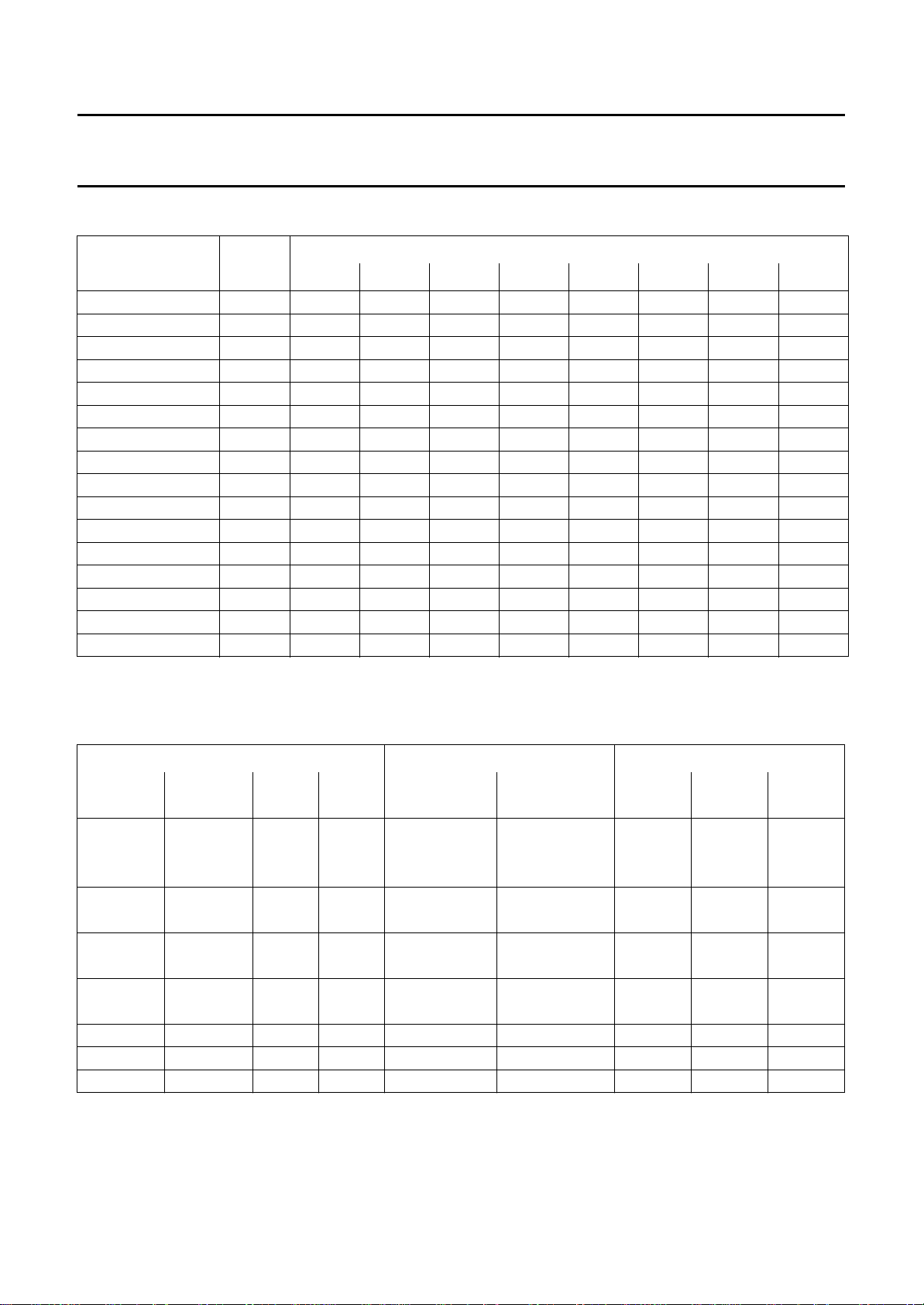
Table 1 Sub-address (SAD) and data bytes
SAD MSB DATA BYTE LSB
FUNCTION
(HED) 7 6 5 4 3210
Brightness 00 0 0 A05 A04 A03 A02 A01 A00
Saturation 01 0 0 A15 A14 A13 A12 A11 A10
Contrast 02 0 0 A25 A24 A23 A22 A21 A20
Hue control voltage 03 0 0 A35 A34 A33 A32 A31 A30
Red gain 04 0 0 A45 A44 A43 A42 A41 A40
Green gain 05 0 0 A55 A54 A53 A52 A51 A50
Blue gain 06 0 0 A65 A64 A63 A62 A61 A60
Reserved 07 0 0 x x x x x x
Reserved 08 0 0 x x x x x x
Reserved 09 0 0 x x x x x x
Peak drive limit 0A 0 0 AA5 AA4 AA3 AA2 AA1 AA0
Reserved 0B x x x x x x x x
Control register 1 0C SC5 x BREN x NMEN x x x
Control register 2 0D x x x BCOF FSDIS2 FSON2 FSDIS1 FSON1
Reserved 0E x x x x x x x x
Reserved 0F x x x x x x x x
(1)
.
Note to Table 1
1. X is ‘don’t care’, but for software compatibility with other or future video ICs it is recommended to set all ‘X’ to ‘0’.
FSW
(pin 1)
(1)
.
2
FSW
1
(pin 13)
RGB
RGB
2
Y/CD
1
Table 2 Signal input selection by the fast source switches
2
C-BUS CONTROL BITS ANALOG SWITCH SIGNALS INPUT SELECTED
I
FSON2 FSDIS2 FSON1 FSDIS1
L L LLL L ON
LH ON
HX ON
LLLHL X ON
HX ON
LLHXL X ON
HX ON
L H LLX L ON
XH ON
LHLHX X ON
LHHXX X ON
H X XXX X ON
Note to Table 2
1. Where L is a logic LOW (< 0.4 V), H is a logic HIGH (> 0.9 V), X is ‘don’t care’, and ON is the selected input signal.
May 1993 9
Page 10
Philips Semiconductors Preliminary specification
Video processor with automatic cut-off
TDA4685
control
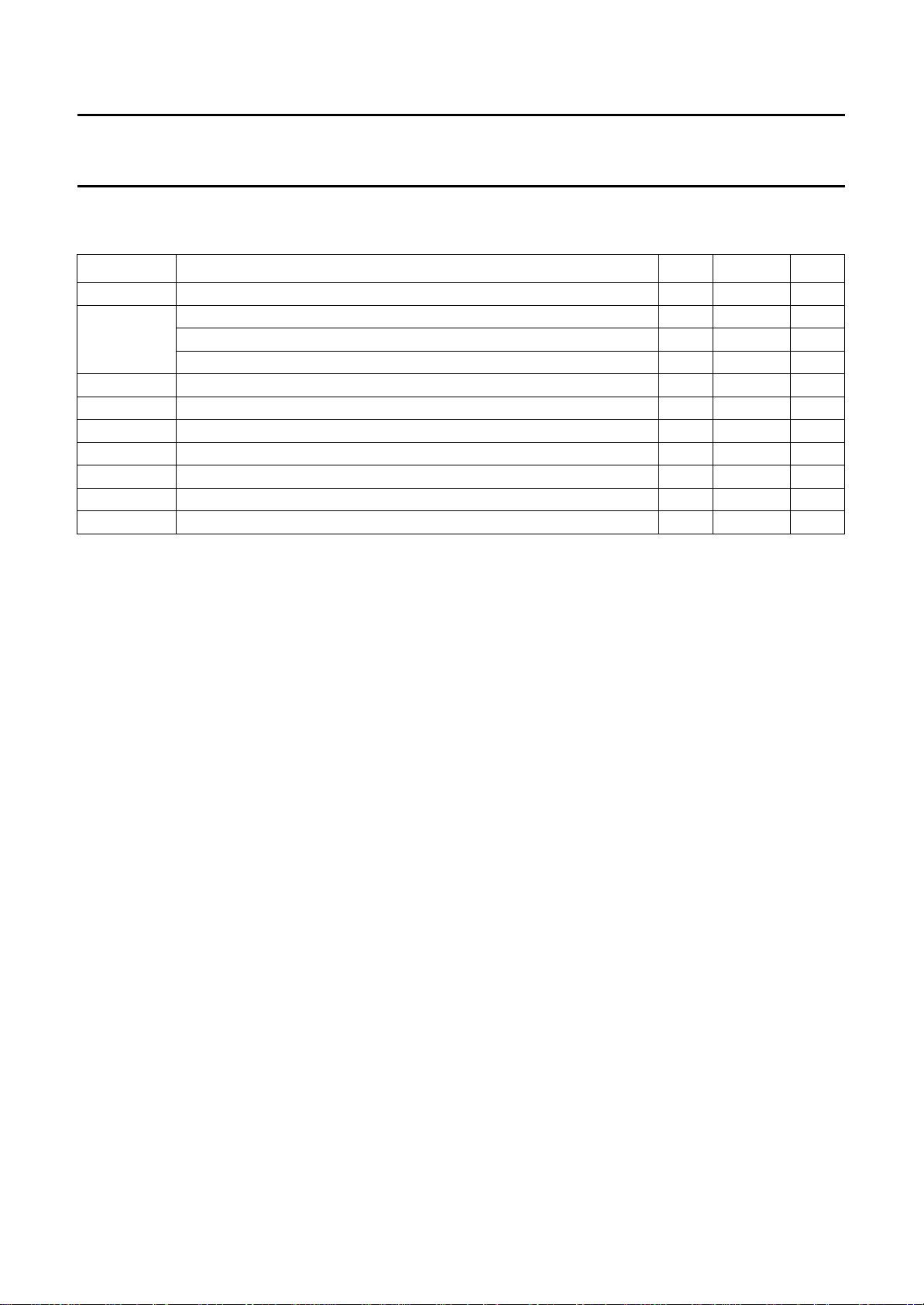
LIMITING VALUES
In accordance with the Absolute Maximum Rating System (IEC134).
SYMBOL PARAMETER MIN. MAX. UNIT
V
P
V
I
V
14
I
AV
I
M
I
26
T
stg
T
amb
P
tot
supply voltage (pin 5) − 8.8 V
input voltage (pins 1 to 8, 10 to 13, 16, 21, 23 and 25) −0.1 V
input voltage (pins 15, 18 and 19) −0.7 V
P
+ 0.7 V
P
input voltage (pins 27 and 28) −0.1 8.8 V
sandcastle pulse voltage −0.7 VP+5.8 V
average current (pins 20, 22 and 24) −10 4 mA
peak current (pins 20, 22 and 24) −20 4 mA
output current −8 0.6 mA
storage temperature −20 +150 °C
operating ambient temperature 0 +70 °C
total power dissipation − 1.2 W
V
May 1993 10
Page 11
Philips Semiconductors Preliminary specification
ha
Video processor with automatic cut-off
control
17
TDA4685
+
MED711
8765 12 13 141110943
TDA4685
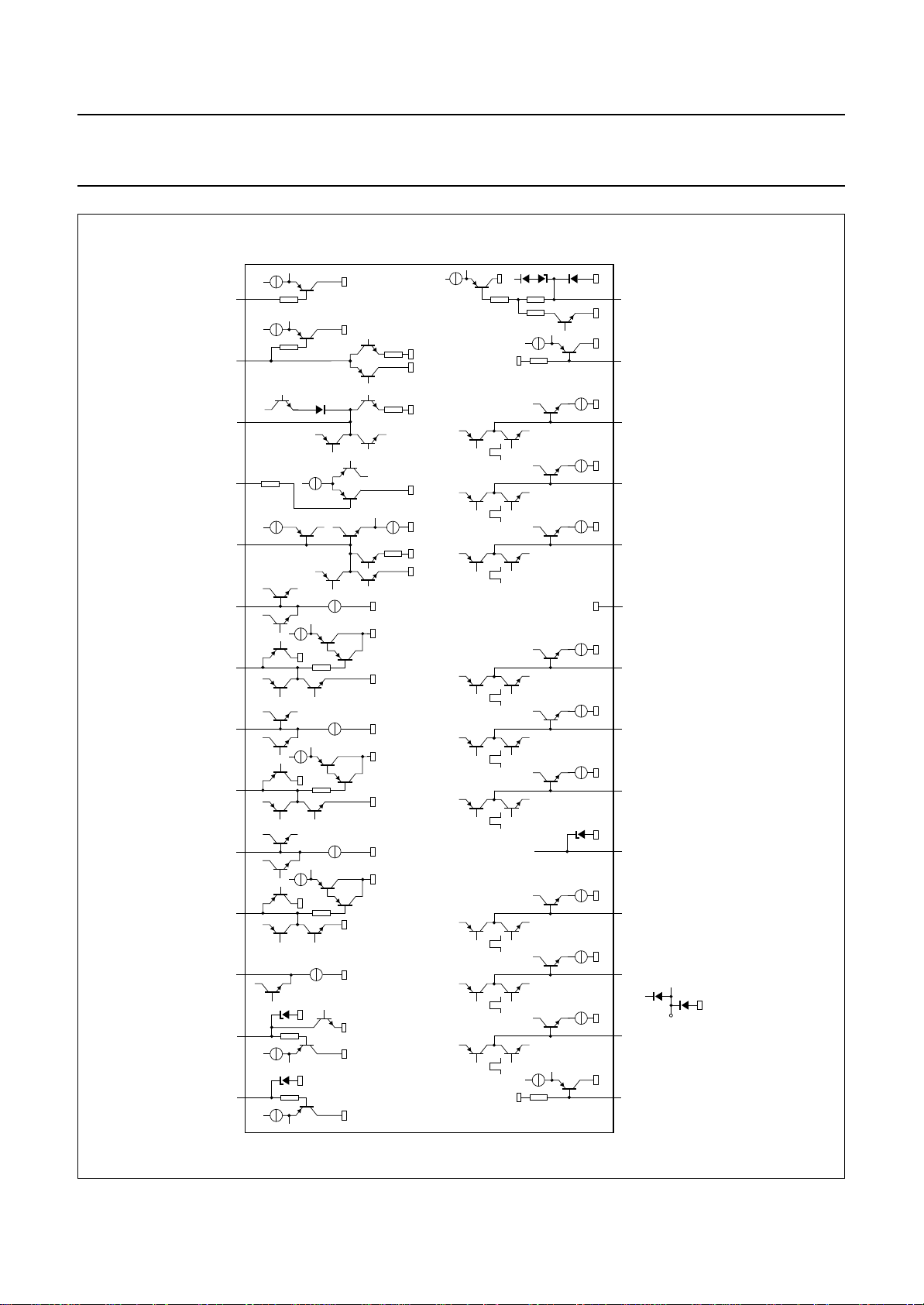
Fig.6 Internal circuits.
23 22 21 20 19 1825 24262728 1516
+
+
2
CL CL CL CLCLCLCLCLCL
1
diode protection
on all pins except
pins 5, 14, 27 and 28
ndbook, full pagewidth
May 1993 11
Page 12
Philips Semiconductors Preliminary specification
Video processor with automatic cut-off
TDA4685
control
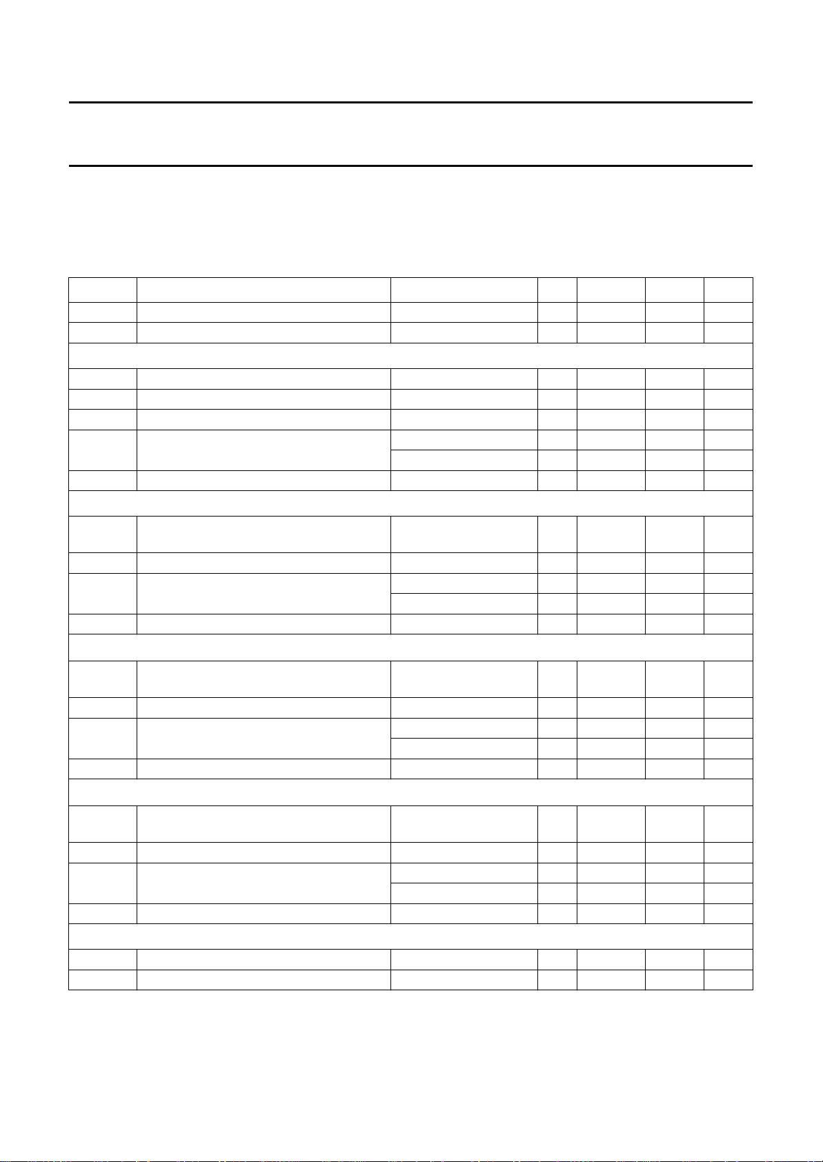
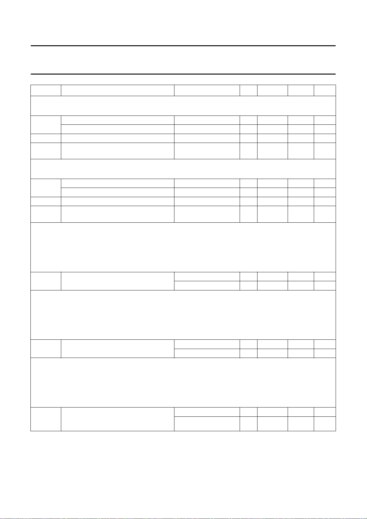
CHARACTERISTICS
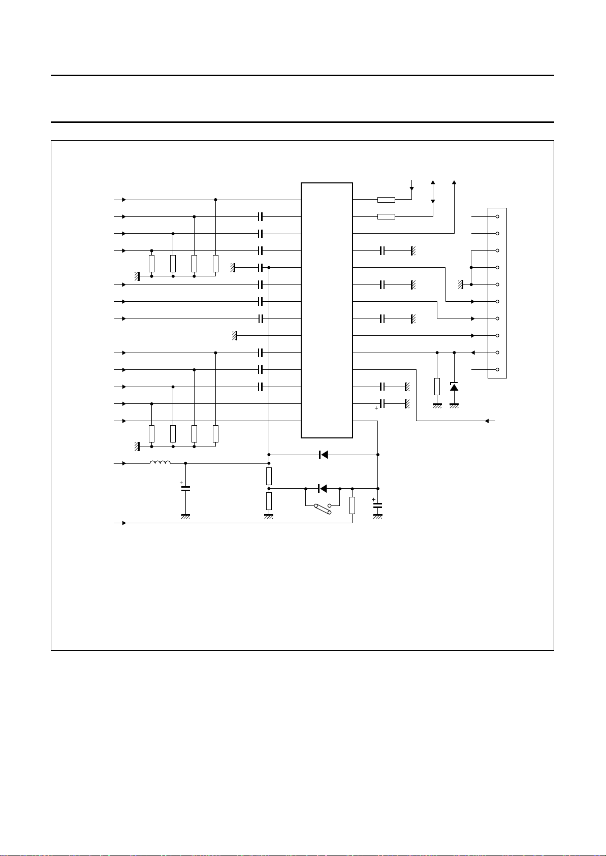
All voltages are measured in test circuit of Fig.7 with respect to GND (pin 9); V
= 8.0 V; T
P
- at nominal signal amplitudes (black-to-white) at output pins 24, 22 and 20,
- at nominal settings of brightness, contrast, saturation and white level control,
- without beam current or peak drive limiting; unless otherwise specified.
SYMBOL PARAMETER CONDITIONS MIN. TYP. MAX. UNIT
V
P
I
P
supply voltage (pin 5) 7.2 8.0 8.8 V
supply current (pin 5) − 60 − mA
Colour difference inputs
V
V
V
I
6,7
6(p-p)
7(p-p)
6,7
−(B−Y) input (peak-to-peak value) notes 1 and 2 − 1.33 − V
−(R−Y) input (peak-to-peak value) notes 1 and 2 − 1.05 − V
internal DC bias voltage at black level clamping − 4.1 − V
input current during line scan −− ±0.1 µA
at black level clamping ±100 −−µA
R
6,7
input resistance 10 −−MΩ
Luminance/sync (VBS)
V
i(p-p)
luminance input at pin 8
note 2 − 0.45 − V
(peak-to-peak value)
V
8
I
8
internal DC bias voltage at black level clamping − 4.1 − V
input current during line scan −− ±0.1 µA
at black level clamping ±100 −−µA
R
8
,G1and B1inputs
R
1
V
i(p-p)
input resistance 10 −−MΩ
black-to-white input signals at pins 10, 11
note 2 − 0.7 − V
and 12 (peak-to-peak value)
V
10/11/12
I
10/11/12
internal DC bias voltage at black level clamping − 5.7 − V
input current during line scan −− ±0.1 µA
at black level clamping ±100 −−µA
R
10/11/12
, G2and B2inputs
R
2
V
i(p-p)
input resistance 10 −−MΩ
black-to-white input signals at pins 2, 3
note 2 − 0.7 − V
and 4 (peak-to-peak value)
V
I
2/3/4
2/3/4
internal DC bias voltage at black level clamping − 5.7 − V
input current during line scan −− ±0.1 µA
at black level clamping ±100 −−µA
R
2/3/4
input resistance 10 −−MΩ
PAL/SECAM and NTSC matrix (note 3)
PAL/SECAM matrix control bit NMEN = 0
NTSC matrix control bit NMEN = 1
amb
=+25 °C:
May 1993 12
Page 13
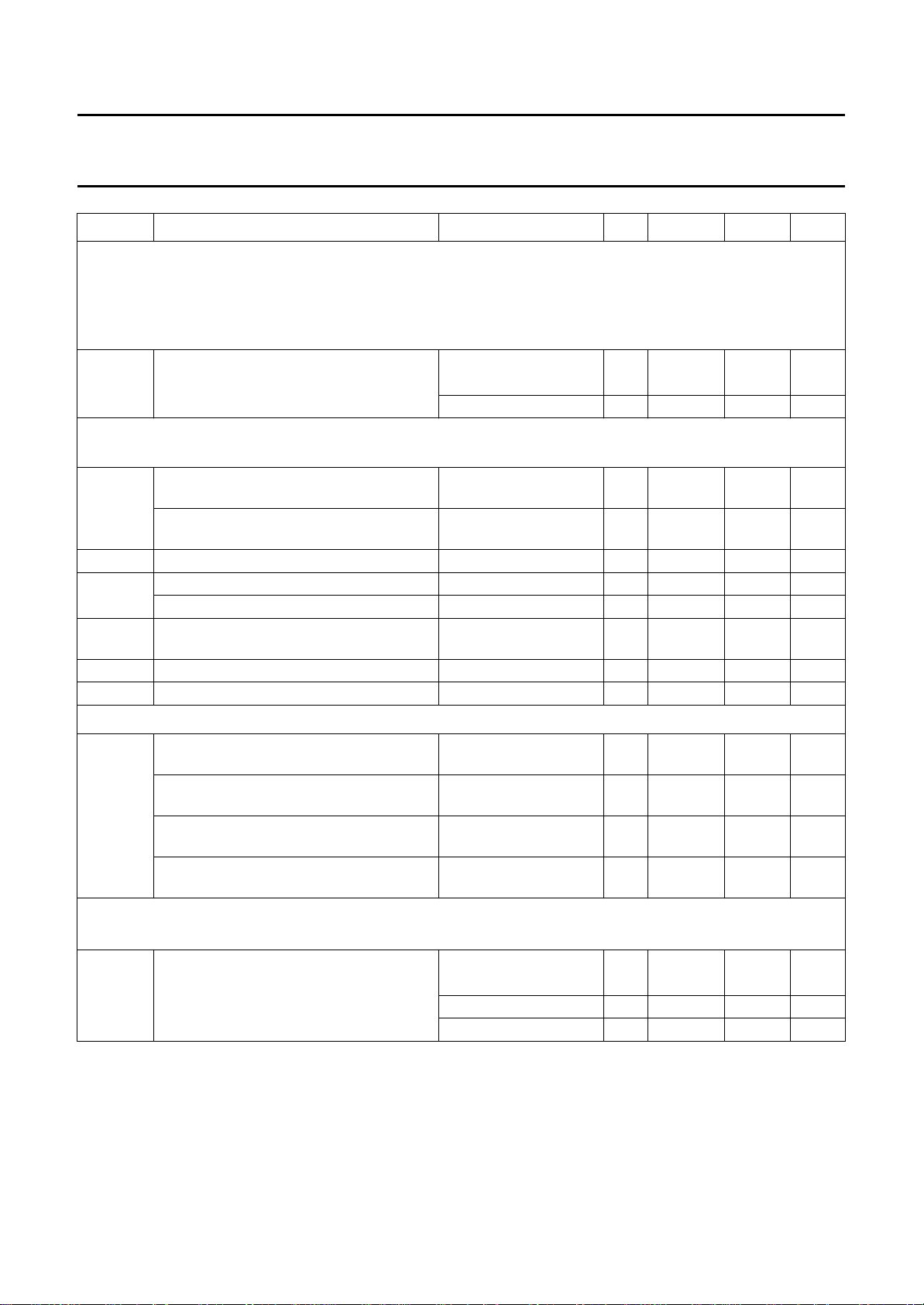
Philips Semiconductors Preliminary specification
Video processor with automatic cut-off
TDA4685
control
SYMBOL PARAMETER CONDITIONS MIN. TYP. MAX. UNIT
Fast signal switch FSW1to select Y, CD or R1, G1,B1inputs
control bits FSDIS1, FSON1 (see Table 2)
V
13
R
13
∆t difference between transit times for
Fast signal switch FSW2 to select Y, CD / R1, G1, B1or R2, G2, B2inputs
control bits FSDIS2, FSON2 (see Table 2)
V
1
R
1
∆t difference between transit times for
Saturation adjust
acts on −(R−Y) and −(B−Y) signals under I
sub-address 01
data byte 3F
data byte 23
data byte 00
d
s
Contrast adjust
acts on internal RGB signals under I
sub-address 02
data byte 3F
data byte 22
data byte 00
d
c
Brightness adjust
acts on internal RGB signals under I
sub-address 00
data byte 3F
data byte 26
data byte 00
d
br
voltage to select Y and CD −− 0.4 V
voltage range to select R
, G1, B
1
1
0.9 − 5.0 V
internal resistance to ground − 4.0 − kΩ
−− 10 ns
signal switching and signal insertion
voltage to select Y, CD/R1,G1, B
voltage range to select R
, G2, B
2
1
2
−− 0.4 V
0.9 − 5.0 V
internal resistance to ground − 4.0 − kΩ
−− 10 ns
signal switching and signal insertion
2
C-bus control,
(bit resolution 1.5% of maximum saturation);
Hex
for maximum saturation
Hex
for nominal saturation
Hex
for minimum saturation
Hex
saturation below maximum at 23
at 00
2
C-bus control,
(bit resolution 1.5% of maximum contrast);
Hex
for maximum contrast
Hex
for nominal contrast
Hex
for minimum contrast
Hex
contrast below maximum at 22
at 00
2
C-bus control,
(bit resolution 1.5% of maximum brightness);
Hex
for maximum brightness
Hex
for nominal brightness
Hex
for minimum brightness
Hex
black level shift of nominal signal
amplitude referred to cut-off
at 3F
at 00
measurement level
Hex
; f = 100 kHz − 50 − dB
Hex
Hex
Hex
Hex
Hex
− 5 − dB
− 5 − dB
− 22 − dB
− 30 − %
−−50 − %
May 1993 13
Page 14
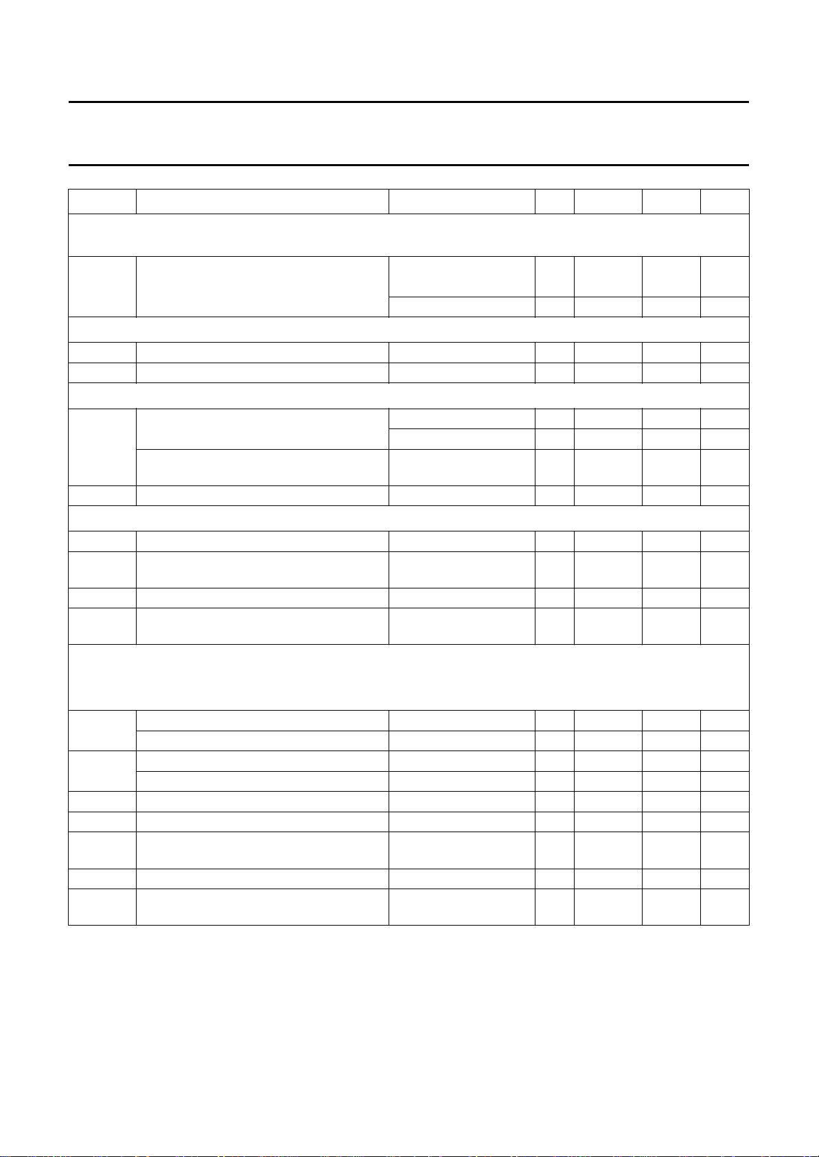
Philips Semiconductors Preliminary specification
Video processor with automatic cut-off
TDA4685
control
SYMBOL PARAMETER CONDITIONS MIN. TYP. MAX. UNIT
White potentiometers, under I2C-bus control,
sub-addresses 04
data byte 3F
data byte 19
data byte 00
∆G
v
Hex
Hex
Hex
relative to nominal gain:
(red), 05
Hex
for maximum gain
for nominal gain
for minimum gain
increase of gain at 3F
decrease of gain at 00
RGB outputs pins 24, 22 and 20
(positive going output signals; peak drive limiter set = 3F
V
o(b-w)
nominal output signal amplitudes
(black-to-white value)
maximum output signal amplitudes
(black-to-white value)
∆V
o
V
o
spread between RGB output signals −− 10 %
minimum output voltages −− 0.8 V
maximum output voltages 6.8 −−V
V
24,22,20
voltage of cut-off measurement line
= voltage during ultra-black
I
int
R
o
internal current sources − 5.0 − mA
output resistance − 20 −Ω
Frequency response
d frequency response of Y path
(from pin 8 to pins 24, 22, 20)
frequency response of CD path
(from pins 7 to 24 and 6 to 20)
frequency response of RGB
pins 10 to 24, 11 to 22 and 12 to 20)
frequency response of RGB
(from pins 2 to 24, 3 to 22 and 4 to 20)
(green) and 06
Hex
path (from
1
path
2
(blue); note 4.
Hex
Hex
BCOF = 1
(output clamping)
f = 10 MHz −− 3dB
f = 8 MHz −− 3dB
f = 10 MHz −− 3dB
f = 10 MHz −− 3dB
Hex
Hex
); note 5.
− 50 − %
− 50 − %
− 2 − V
3.0 −−V
2.3 2.5 2.7 V
Sandcastle pulse detector (control bit SC5 = 0)
three level; notes 6 and 7
V
14
required voltage range
for H and V blanking pulses 2.0 2.5 3.0 V
for H pulses (line count) 4.0 4.5 5.0 V
for burst key pulses (clamping) 7.6 − V
May 1993 14
+5.8 V
P
Page 15
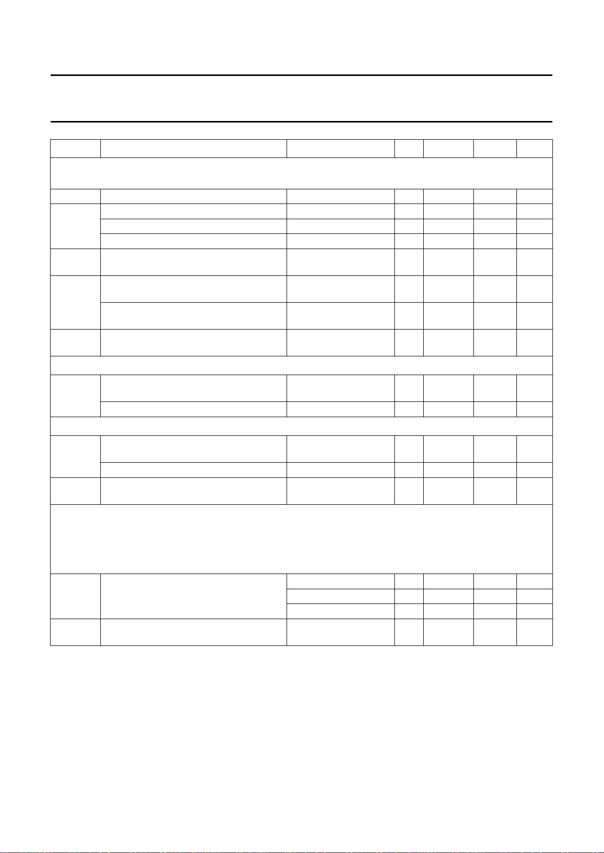
Philips Semiconductors Preliminary specification
Video processor with automatic cut-off
TDA4685
control
SYMBOL PARAMETER CONDITIONS MIN. TYP. MAX. UNIT
Sandcastle pulse detector (control bit SC5 = 1)
two level; notes 6 and 7
V
14
Sandcastle pulse detector
I
14
t
d
VFB (note 7)
V
18
I
18
Average beam current limiting (note 9)
V
c(15)
∆V
c(15)
V
br(15)
∆V
br(15)
required voltage range
for H and V blanking pulses 2.0 2.5 3.0 V
for burst key pulses 4.0 4.5 V
+5.8 V
P
output current V14= 0 V −− −100 µA
leading edge delay of the clamping pulse − 1.5 −µs
vertical flyback pulse for LOW −− 2.5 V
for HIGH 4.5 −−V
internal voltage pin 18 open-circuit;
− 5.0 − V
note 8
input current −− 5 µA
contrast reduction starting voltage − 4.0 − V
voltage difference for full contrast
−−2.0 − V
reduction
brightness reduction starting voltage − 2.5 − V
voltage difference for full brightness
−−1.6 − V
reduction
Peak drive limiting voltage (note 10)
internal peak drive limiting level (V
2
C-bus control, sub-address 0A
I
V
20/22/24
level for minimum RGB outputs at byte 00
pdl
Hex
level for maximum RGB outputs at byte 3F
I
16
charge current −−1 −µA
discharge current during peak white − 5 − mA
V
16
V
c(16)
∆V
c(16)
internal voltage limitation 4.5 −−V
contrast reduction starting voltage − 4.0 − V
voltage difference for full contrast
reduction
V
∆V
br(16)
br(16)
brightness reduction starting voltage − 2.5 − V
voltage difference for full brightness
reduction
) acts on RGB outputs
Hex
Hex
−− 3.0 V
7.0 −−V
−−2.0 − V
−−1.6 − V
May 1993 15
Page 16
Philips Semiconductors Preliminary specification
Video processor with automatic cut-off
TDA4685
control
SYMBOL PARAMETER CONDITIONS MIN. TYP. MAX. UNIT
Automatic cut-off control (notes 7, 11, 12 and 13)
see Fig.9
V
19
I
19
external voltage −− V
output current −− −60 µA
input current 150 −−µA
additional input current switch-on delay 1 − 0.5 − mA
V
24,22,20
monitor pulse amplitude (under
I2C-bus control, sub-address 0A
V
19
voltage threshold for picture tube
cathode warm-up
internally controlled voltage (V
∆V
19
voltage difference between V
(cut-off measurement voltage) and V
Cut-off storage
I
21/23/25
charge and discharge currents during cut-off
current outside measurement −− ±0.1 µA
switch-on delay 1;
Hex
)
note 12
switch-on delay 1 − 4.5 − V
) during leakage
REF
measurement period
MEAS
REF
measurement lines
− V
− 1.0 − V
pdl
− 2.7 − V
− 1.0 − V
−±0.3 − mA
- 1.4 V
P
Leakage storage
I
17
charge and discharge currents during leakage
current outside measurement −− ±0.1 µA
V
17
threshold voltage for reset to switch-on
state
Hue control (note 14)
2
under I
data byte 3F
data byte 20
data byte 00
V
I
int
C-bus control, sub-address 03
for maximum voltage
Hex
for nominal voltage
Hex
for minimum voltage
Hex
26
output voltage at byte 3F
current of the internal current source at
pin 26
Hex
measurement period
Hex
at byte 20
at byte 00
Hex
Hex
−±0.4 − mA
− 2.5 − V
4.8 −−V
− 3.0 − V
−− 1.2 V
500 −−µA
May 1993 16
Page 17
Philips Semiconductors Preliminary specification
Video processor with automatic cut-off
TDA4685
control
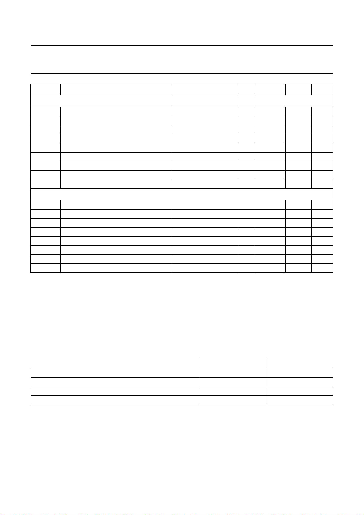
SYMBOL PARAMETER CONDITIONS MIN. TYP. MAX. UNIT
2
I
C-bus receiver clock SCL (pin 28)
f
SCL
V
IL
V
IH
I
IL
I
IH
t
d
t
r
t
f
2
C-bus receiver data input/output SDA (pin 27)
I
V
IL
V
IH
I
IL
I
IH
I
OL
t
r
t
f
t
SU;DAT
Notes to the characteristics
1. The values of the −(B−Y) and −(R−Y) colour difference input signals are for a 75% colour-bar signal.
2. The pins are capacitively coupled to a low ohmic source, with a recommended maximum output impedance of 600Ω.
3. PAL/SECAM signals are matrixed by the equation: V
NTSC signals are matrixed by the equations (hue phase shift of −5 degrees):
V
R−Y*
In the matrix equations: V
NTSC demodulator. V
the following demodulator axes and amplification factors:
input frequency range 0 − 100 kHz
LOW level input voltage −− 1.5 V
HIGH level input voltage 3.0 − 6.0 V
LOW level input current −− −10 µA
HIGH level input current −− 10 µA
pulse delay time LOW 4.7 −−µs
pulse delay time HIGH 4.0 −−µs
rise time −− 1.0 µs
fall time −− 0.3 µs
LOW level input voltage −− 1.5 V
HIGH level input voltage 3.0 − 6.0 V
LOW level input current −− −10 µA
HIGH level input current −− 10 µA
LOW level output current 3.0 −−mA
rise time −− 1.0 µs
fall time −− 0.3 µs
data set-up time 0.25 −−µs
= 1.57V
R−Y
- 0.41V
G−Y
B−Y
R−Y
*, V
; V
G−Y
and V
R−Y
=− 0.51V
G−Y
* = −0.43V
are conventional PAL demodulation axes and amplitudes at the output of the
B−Y
* and V
B−Y
R−Y
− 0.11V
B−Y
; V
* are the NTSC-modified colour difference signals; this is equivalent to
B−Y
R−Y
* = V
− 0.19V
B−Y
B−Y
(B−Y)* demodulator axis 0° 0°
(R−Y)* demodulator axis 115° 90°
(R−Y)* amplification factor 1.97 1.14
(B−Y)* amplification factor 2.03 2.03
V
* = −0.27V
G−Y
R−Y
4. The white potentiometers affect the amplitudes of the RGB output signals.
5. The RGB outputs at pins 24, 22 and 20 are emitter followers with current sources.
May 1993 17
* − 0.22V
B−Y
NTSC PAL
*.
Page 18

Philips Semiconductors Preliminary specification
Video processor with automatic cut-off
TDA4685
control
6. Sandcastle pulses are compared with internal threshold voltages independent of VP. The threshold voltages
separate the components of the sandcastle pulse. The particular component is generated when the voltage on
pin 14 exceeds the defined internal threshold voltage. The internal threshold voltages (control bit SC5 = 0) are:
1.5 V for horizontal and vertical blanking pulses (H and V blanking pulses),
3.5 V for horizontal pulses,
6.5 V for the burst key pulse.
The internal threshold voltages, control bit SC5 = 1, are:
1.5 V for horizontal and vertical blanking pulses,
3.5 V for the burst key pulse.
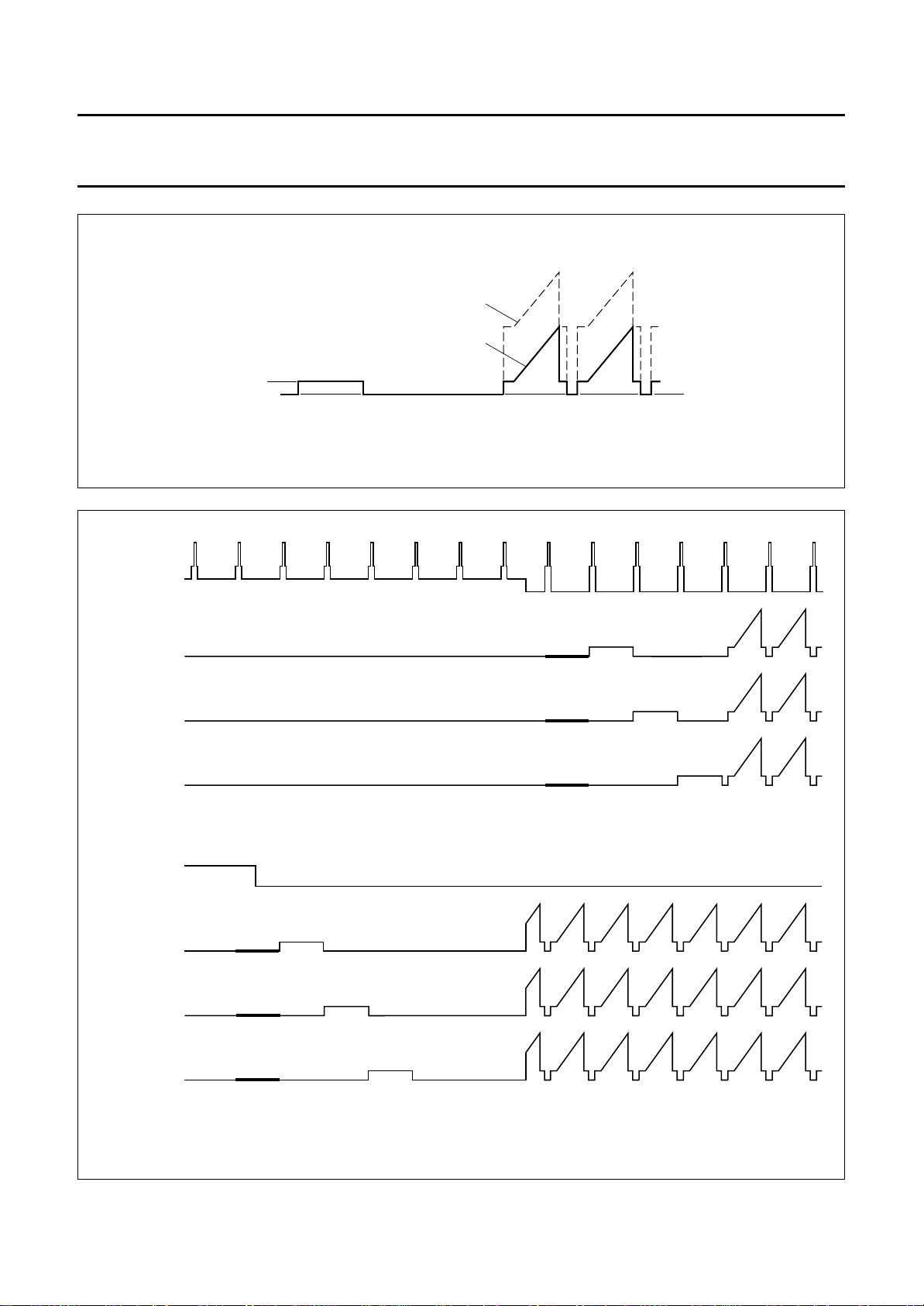
7. Vertical signal blanking is determined by the vertical component of the sandcastle pulse. The leakage and the RGB
cut-off measurement lines are positioned in the first four complete lines after the end of the vertical component. In
this case, the RGB output signals are blanked until the end of the last measurement line; see Fig 9(a). If an extra
vertical flyback pulse VFB is applied to pin 18, the four measurement lines start in the first complete line after the end
of the VFB pulse; see Fig 9(b). In this case, the output signals are blanked either until the end of the last
measurement line or until the end of the vertical component of the sandcastle pulse, according to which occurs last.
8. If no VFB pulse is applied, pin 18 can be left open-circuit or connected to VP. If pin 18 is always LOW neither
automatic cut-off control nor output clamping can happen.
9. Average beam current limiting reduces the contrast, at minimum contrast it reduces the brightness.
10. Peak drive limiting reduces the RGB outputs by reducing the contrast, at minimum contrast it reduces the brightness.
The maximum RGB outputs are determined via the I2C-bus under sub-address 0A
the maximum voltage, peak drive limiting is delayed by one horizontal line.
11. During leakage current measurement, the RGB channels are blanked to ultra-black level. During cut-off
measurement one channel is set to the measurement pulse level, the other channels are blanked to ultra-black.
Since the brightness adjust shifts the colour signal relative to the black level, the brightness adjust is disabled during
the vertical blanking interval (see Fig.8 and Fig.9).
12. During picture cathode warm-up (first switch-on delay) the RGB outputs (pins 24, 22 and 20) are blanked to the
ultra-black level during line scan. During the vertical blanking interval a white-level monitor pulse is fed out on the
RGB outputs and the cathode currents are measured. When the voltage threshold on pin 19 is greater than 4.5 V,
the monitor pulse is switched off and cut-off control is activated (second switch-on delay). As soon as cut-off control
stabilizes, RGB output blanking is removed.
13. The cut-off measurement level range at the RGB outputs is 1 to 5 V. The recommended value is 3 V.
14. The hue control output at pin 26 is an emitter follower with current source.
. When an RGB output exceeds
Hex
May 1993 18
Page 19
Philips Semiconductors Preliminary specification
Video processor with automatic cut-off
control
handbook, full pagewidth
FSW
2
R
2
G
2
B
2
−(B−Y)
−(R−Y)
Y
R
1
G
1
B
1
FSW
1
SC
VP = 8 V
beam
current
information
10 nF
10 nF
10 nF
75
75
75
Ω
Ω
75
75
Ω
Ω
22 µH
220 µF
75
Ω
Ω
75
75
Ω
Ω
10 nF
10 nF
10 nF
47 nF
10 nF
10 nF
10 nF
3.9 kΩ
3.9 kΩ
FSW
R
G
B
V
−(B−Y)
−(R−Y)
GND
R
G
B
FSW
SC
1N4148
1N4148
2
2
2
2
P
Y
1
1
1
1
1
2
3
4
5
6
7
TDA4685
8
9
10
11
12
13
14
(1)
BR1
TDA4685
SCL SDA hue
100 Ω
SCL
28
100 Ω
SDA
27
HUE
26
C
25
R
24
C
23
G
22
C
21
B
20
CI
19
V
18
C
17
C
16
BCL
15
10
kΩ
R
O
G
O
B
O
FB
L
PDL
220 nF
220 nF
220 nF
330 nF
1 µF
22 µF
82
kΩ
BZX79
C6V2
10
1
2
3
4
5
6
7
8
9
CON2
VFB
(optional)
200 V
+12 V
GND
R
o
G
o
B
o
CI
MED712
May 1993 19
(1) Insert link BR1 if average beam
current limiting is not applied.
Fig.7 Test and application circuit.
Page 20
Philips Semiconductors Preliminary specification
Video processor with automatic cut-off
control
handbook, full pagewidth
maximum brightness
nominal brightness
cut-off measurement line
for red signal
Fig.8 Cut-off measurement pulse.
andbook, full pagewidth
sandcastle pulse
with vertical
component
TDA4685
MED713
ultra-black
R channel
G channel
B channel
vertical flyback
pulse (VFB)
R channel
G channel
B channel
LM
LM
LM
MR
LM
MR
LM
LM
(a) Timing controlled by sandcastle pulse
LM = leakage current measurement time
MR, MG, MB = R, G, B cutt-off measurement pulses
MG
MB
(b) Timing controlled by additional vertical flyback pulse (VFB)
MG
MB
MED714
May 1993 20
Fig.9 Leakage and cut-off current measurement timing diagram.
Page 21
Philips Semiconductors Preliminary specification
Video processor with automatic cut-off
control
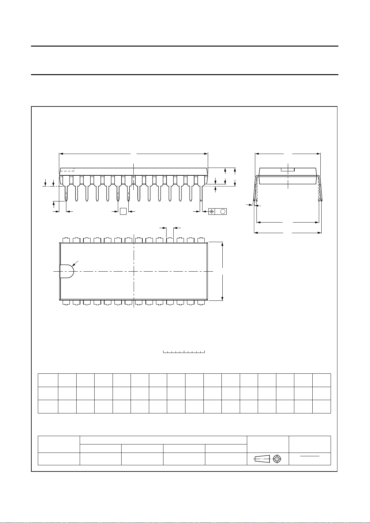
PACKAGE OUTLINE
handbook, full pagewidth
DIP28: plastic dual in-line package; 28 leads (600 mil)
D
seating plane
L
Z
28
e
b
TDA4685
SOT117-1
M
E
A
2
A
A
1
w M
b
1
15
c
(e )
1
M
H
pin 1 index
1
0 5 10 mm
scale
DIMENSIONS (inch dimensions are derived from the original mm dimensions)
A
A
A
UNIT
inches
Note
1. Plastic or metal protrusions of 0.25 mm maximum per side are not included.
max.
mm
1 2
min.
max.
b
1.7
1.3
0.066
0.051
b
0.53
0.38
0.020
0.014
cD E weM
1
0.32
0.23
0.013
0.009
(1) (1)
36.0
35.0
1.41
1.34
14.1
13.7
0.56
0.54
E
14
(1)
L
3.9
3.4
M
E
15.80
15.24
0.62
0.60
H
17.15
15.90
0.68
0.63
0.252.54 15.24
0.010.10 0.60
e
1
0.15
0.13
Z
max.
1.75.1 0.51 4.0
0.0670.20 0.020 0.16
OUTLINE
VERSION
SOT117-1
May 1993 21
REFERENCES
IEC JEDEC EIAJ
051G05 MO-015AH
EUROPEAN
PROJECTION
ISSUE DATE
92-11-17
95-01-14
Page 22

Philips Semiconductors Preliminary specification
Video processor with automatic cut-off
control
SOLDERING
Introduction
There is no soldering method that is ideal for all IC
packages. Wave soldering is often preferred when
through-hole and surface mounted components are mixed
on one printed-circuit board. However, wave soldering is
not always suitable for surface mounted ICs, or for
printed-circuits with high population densities. In these
situations reflow soldering is often used.
This text gives a very brief insight to a complex technology.
A more in-depth account of soldering ICs can be found in
“IC Package Databook”
our
Soldering by dipping or by wave
The maximum permissible temperature of the solder is
260 °C; solder at this temperature must not be in contact
DEFINITIONS
(order code 9398 652 90011).
TDA4685
with the joint for more than 5 seconds. The total contact
time of successive solder waves must not exceed
5 seconds.
The device may be mounted up to the seating plane, but
the temperature of the plastic body must not exceed the
specified maximum storage temperature (T
printed-circuit board has been pre-heated, forced cooling
may be necessary immediately after soldering to keep the
temperature within the permissible limit.
Repairing soldered joints
Apply a low voltage soldering iron (less than 24 V) to the
lead(s) of the package, below the seating plane or not
more than 2 mm above it. If the temperature of the
soldering iron bit is less than 300 °C it may remain in
contact for up to 10 seconds. If the bit temperature is
between 300 and 400 °C, contact may be up to 5 seconds.
stg max
). If the
Data sheet status
Objective specification This data sheet contains target or goal specifications for product development.
Preliminary specification This data sheet contains preliminary data; supplementary data may be published later.
Product specification This data sheet contains final product specifications.
Limiting values
Limiting values given are in accordance with the Absolute Maximum Rating System (IEC 134). Stress above one or
more of the limiting values may cause permanent damage to the device. These are stress ratings only and operation
of the device at these or at any other conditions above those given in the Characteristics sections of the specification
is not implied. Exposure to limiting values for extended periods may affect device reliability.
Application information
Where application information is given, it is advisory and does not form part of the specification.
LIFE SUPPORT APPLICATIONS
These products are not designed for use in life support appliances, devices, or systems where malfunction of these
products can reasonably be expected to result in personal injury. Philips customers using or selling these products for
use in such applications do so at their own risk and agree to fully indemnify Philips for any damages resulting from such
improper use or sale.
2
PURCHASE OF PHILIPS I
C COMPONENTS
May 1993 22
Purchase of Philips I
components in the I2C system provided the system conforms to the I2C specification defined by
Philips. This specification can be ordered using the code 9398 393 40011.
2
C components conveys a license under the Philips’ I2C patent to use the
 Loading...