

Page 1

INTEGRATED CIRCUITS
DATA SH EET
TDA3603
Multiple voltage regulator with
switch
Preliminary specification
Supersedes data of 1995 Feb 16
File under Integrated Circuits, IC01
1995 Oct 04
Page 2

Philips Semiconductors Preliminary specification
Multiple voltage regulator with switch TDA3603
FEATURES
• One VP state controlled regulator (regulator 2)
• Regulator 2, reset and ignition buffer operates during
load dump and thermal shutdown
• One control pin for switching regulator 1 and the power
switch
• Supply voltage range of −18 to +50 V (operating
from 9.75 V)
• Low reverse current of regulator 2
• Low quiescent current (when regulator 1 is switched off,
standby)
• Ignition input/output
• Reset output
• High ripple rejection
• Power switch.
PROTECTIONS
• Reverse polarity safe (down to −18 V without high
reverse current)
• Able to withstand voltages up to 18 V at the outputs
(supply line may be shortened)
• ESD protected on all pins
• Thermal protection
• Load dump protection
• Foldback current limit protection for regulators 1 and 2
• Delayed second current limit protection for the power
switch
• The regulator outputs and the power switch are DC
short-circuited safe to ground and V
.
P
GENERAL DESCRIPTION
The TDA3603 is a multiple output voltage regulator with a
power switch, intended for use in car radios with or without
a microcontroller.
It contains one fixed voltage regulator with a foldback
current protection (regulator 1) and one fixed voltage
regulator (regulator 2), intended to supply a
microcontroller, that also operates during load dump and
thermal shutdown.
There is a power switch with protections, operated by the
enable input.
The reset and ignition outputs can be used to interface by
the microcontroller. The reset signal can be used to call up
the microcontroller and the ignition output indicates
ignition voltage available.
The supply pin can withstand load dump pulses and
negative supply voltages.
Regulator 2 will be switched on at a supply voltage >6.5 V
and off at a voltage of regulator 2 <1.9 V.
ORDERING INFORMATION
TYPE NUMBER
TDA3603 SIL9MPF plastic single in-line medium power package with fin; 9 leads SOT110-1
TDA3603P HDIP18 plastic heat-dissipating dual in-line package; 18 leads SOT398-1
1995 Oct 04 2
PACKAGE
NAME DESCRIPTION VERSION
Page 3
Philips Semiconductors Preliminary specification
Multiple voltage regulator with switch TDA3603
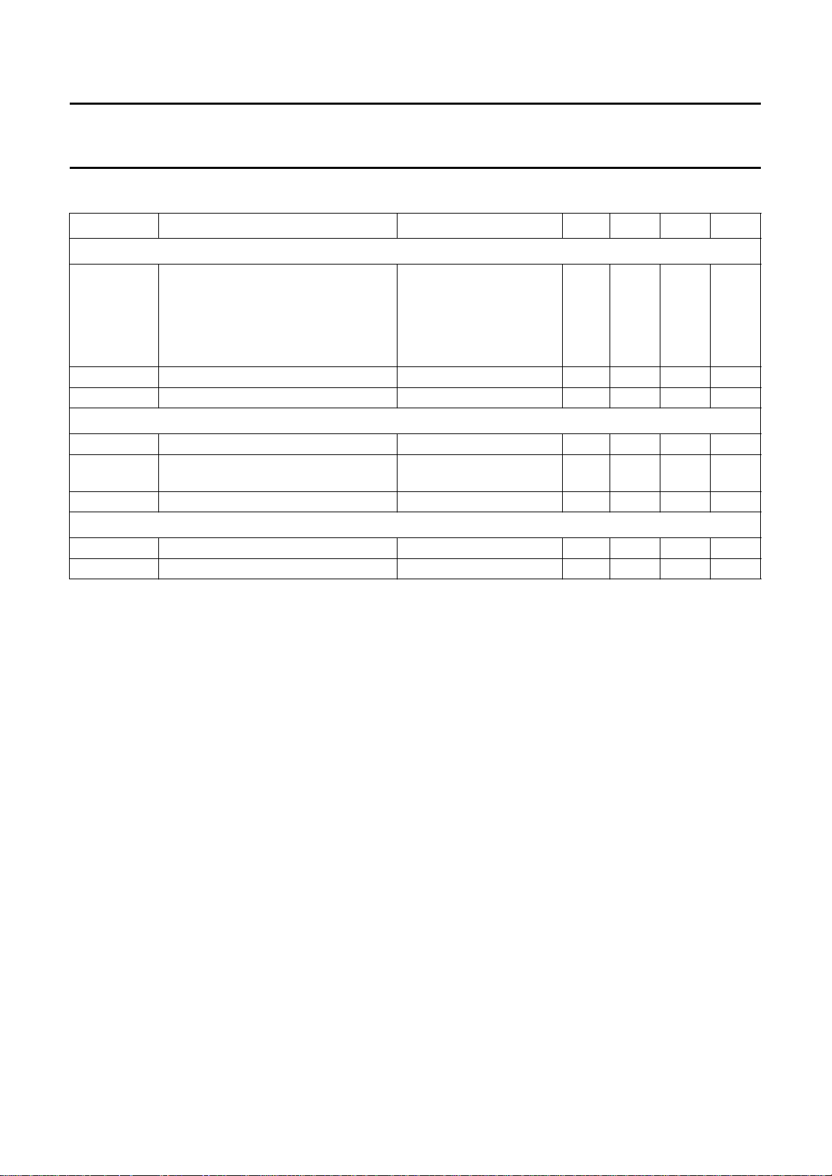
QUICK REFERENCE DATA
SYMBOL PARAMETER CONDITIONS MIN. TYP. MAX. UNIT
Supply
V
P
I
q
T
vj
Voltage regulators
V
REG1
V
REG2
V
drop(REG1)
Power switch
V
drop(sw)
I
M
supply voltage
operating 9.75 14.4 25 V
regulator 2 on note 1 2.4 14.4 25 V
jump start t ≤ 10 minutes −−30 V
load dump protection during 50 ms; t
≥ 2.5 ms −− 50 V
r
total quiescent current standby mode − 400 500 µA
operating virtual junction temperature −−150 °C
output voltage regulator 1 0.5 mA ≤ I
output voltage regulator 2 0.5 mA ≤ I
≤ 300 mA 8.65 9.0 9.35 V
REG1
REG2
≤ 30 mA;
4.8 5.0 5.2 V
VP= 14.4 V
drop-out voltage I
= 0.3 A; note 2 −−0.5 V
REG1
drop-out voltage Isw= 0.3 A; note 3 −−0.9 V
peak current t ≤ 10 ms 1.4 −−A
Notes
1. Minimum operating voltage, only if V
2. The drop-out voltage of regulator 1 is measured between VPand V
has exceeded 6.5 V.
P
REG1.
3. The drop-out voltage of the power switch is measured between VPand Vsw.
1995 Oct 04 3
Page 4
Philips Semiconductors Preliminary specification
Multiple voltage regulator with switch TDA3603
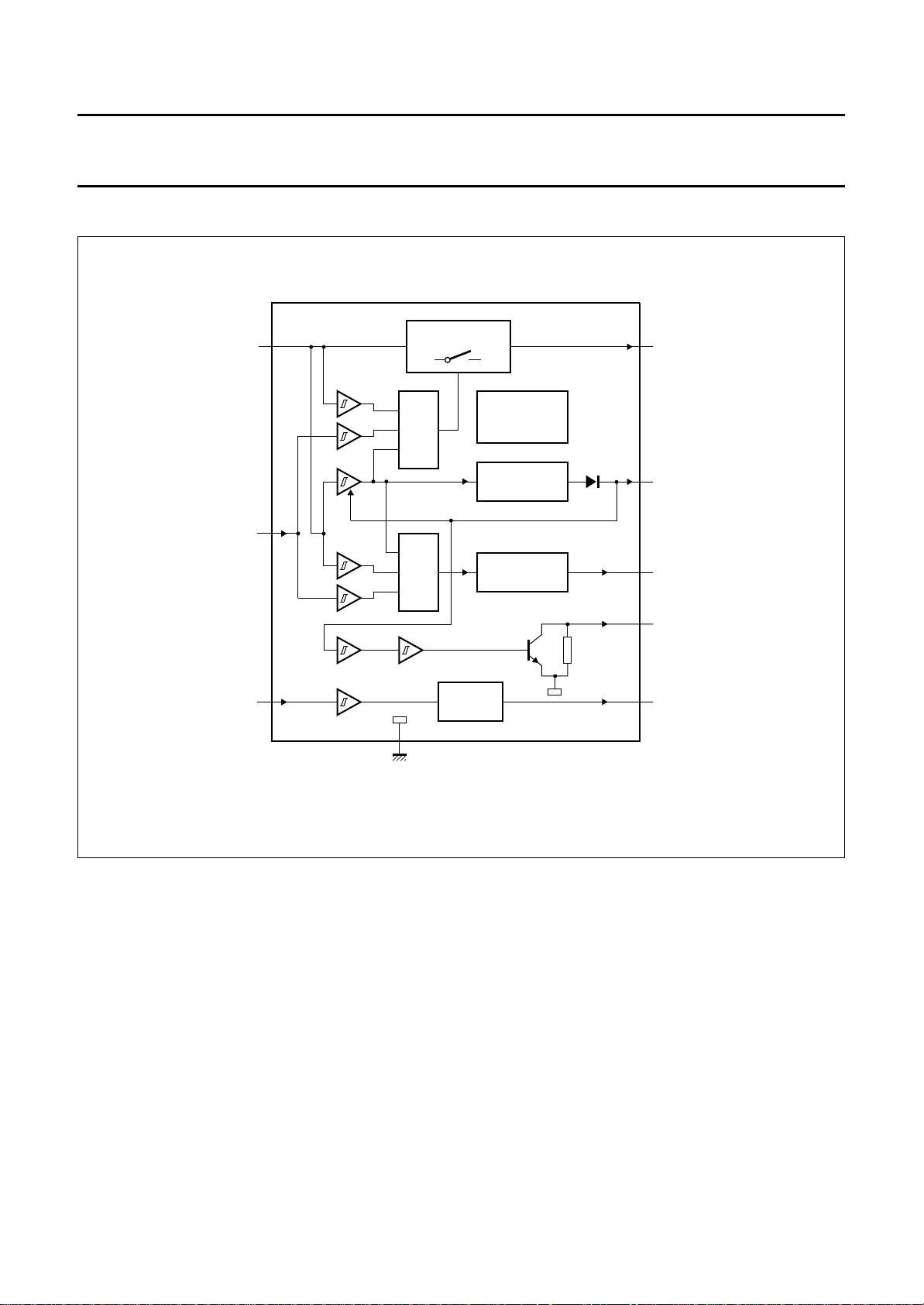
BLOCK DIAGRAM
handbook, full pagewidth
V
P
(14.4 V)
V
1
4
en
POWER SWITCH
TEMPERATURE
&
PROTECTION
REGULATOR 2
LOAD DUMP
9
7
V
sw
(14.0 V/0.3 A)
REG2
(5 V/30 mA)
&
REGULATOR 1
TDA3603
l(ig)
8
V
IGNITION
BUFFER
6
ground
2
3
5
MBE231
REG1
(9 V/300 mA)
RES
(5 V)
V
O(ig)
Fig.1 Block diagram.
1995 Oct 04 4
Page 5
Philips Semiconductors Preliminary specification
Multiple voltage regulator with switch TDA3603
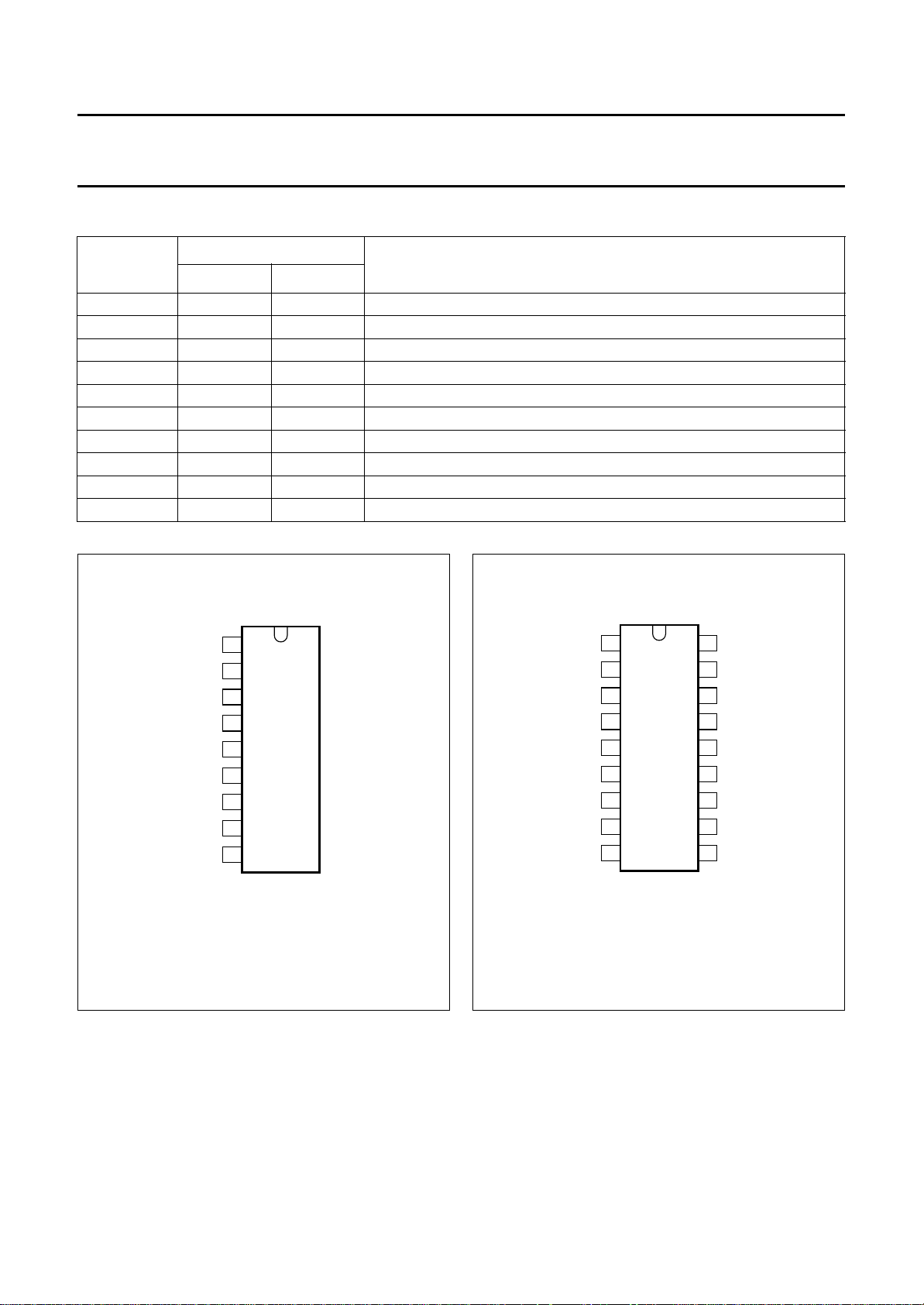
PINNING
SYMBOL
V
P
SOT110-1
SOT398-1
1 1 supply voltage
DESCRIPTION
REG1 2 2 regulator 1 output
RES 3 3 reset output voltage (+5 V)
PIN
V
V
en
O(ig)
4 4 enable input voltage
5 5 ignition output voltage
GND 6 6 ground (0 V)
REG2 7 7 regulator 2 output
V
I(ig)
V
sw
8 8 ignition input voltage
9 9 power switch output voltage
i.c. − 10 to 18 can be connected to a heat spreader
handbook, halfpage
V
REG1
RES
V
V
O(ig)
GND
REG2
V
I(ig)
V
sw
1
P
2
3
4
en
5
TDA3603
6
7
8
9
MBE230
handbook, halfpage
V
REG1
RES
V
V
O(ig)
GND
REG2
V
I(ig)
V
P
en
sw
1
2
3
4
5
TDA3603P
6
7
8
9
MBE229
i.c.
18
i.c.
17
16
i.c.
i.c.
15
i.c.
14
i.c.
13
i.c.
12
i.c.
11
i.c.
10
Fig.2 Pin configuration for SOT110-1.
1995 Oct 04 5
Pins 10 to 18 can be connected to a heat spreader.
Fig.3 Pin configuration for SOT398-1.
Page 6

Philips Semiconductors Preliminary specification
Multiple voltage regulator with switch TDA3603
FUNCTIONAL DESCRIPTION
The TDA3603 is a multiple output voltage regulator with a
power switch, intended for use in car radios with or without
a microcontroller. Because of low-voltage operation of the
car radio, low-voltage drop regulators are used.
Regulator 2 will switch on when the supply voltage
exceeds 6.5 V for the first time and will switch off again
when the output voltage of regulator 2 is below 1.9 V (this
is below an engine start). When regulator 2 is switched on
and the output voltage of this regulator is within its voltage
range, the reset output will be enabled (reset will go HIGH
via a pull-up resistor) to generate a reset to the
microcontroller. The reset cycles can be extended by an
external capacitor at the reset output (pin 3). The start-up
feature is built-in to ensure a smooth start-up of the
microcontroller at first connection, without uncontrolled
switching of regulator 2 during the start-up sequence.
When both regulator 2 and the supply voltage (V
are available, regulator 1 and the switch can be operated
by an enable input (pin 4).
> 4.5 V)
P
All output pins are fully protected. The regulators are
protected against load dump (regulator 1 will switch off at
supply voltages higher than 25 V) and short-circuit
(foldback current protection).
The switch contains a current protection which is delayed
for ≥10 ms (in short-circuit condition). During this time the
current is limited to 1.4 A (V
At supply voltages over 16.9 V the switch is clamped at
15.0 V (to avoid externally connected circuitry being
damaged by an overvoltage) and the switch will switch off
at load dump.
Interfacing with the microcontroller can be accomplished
by an ignition Schmitt-trigger and ignition output buffer,
(simple full/semi on/off logic applications).
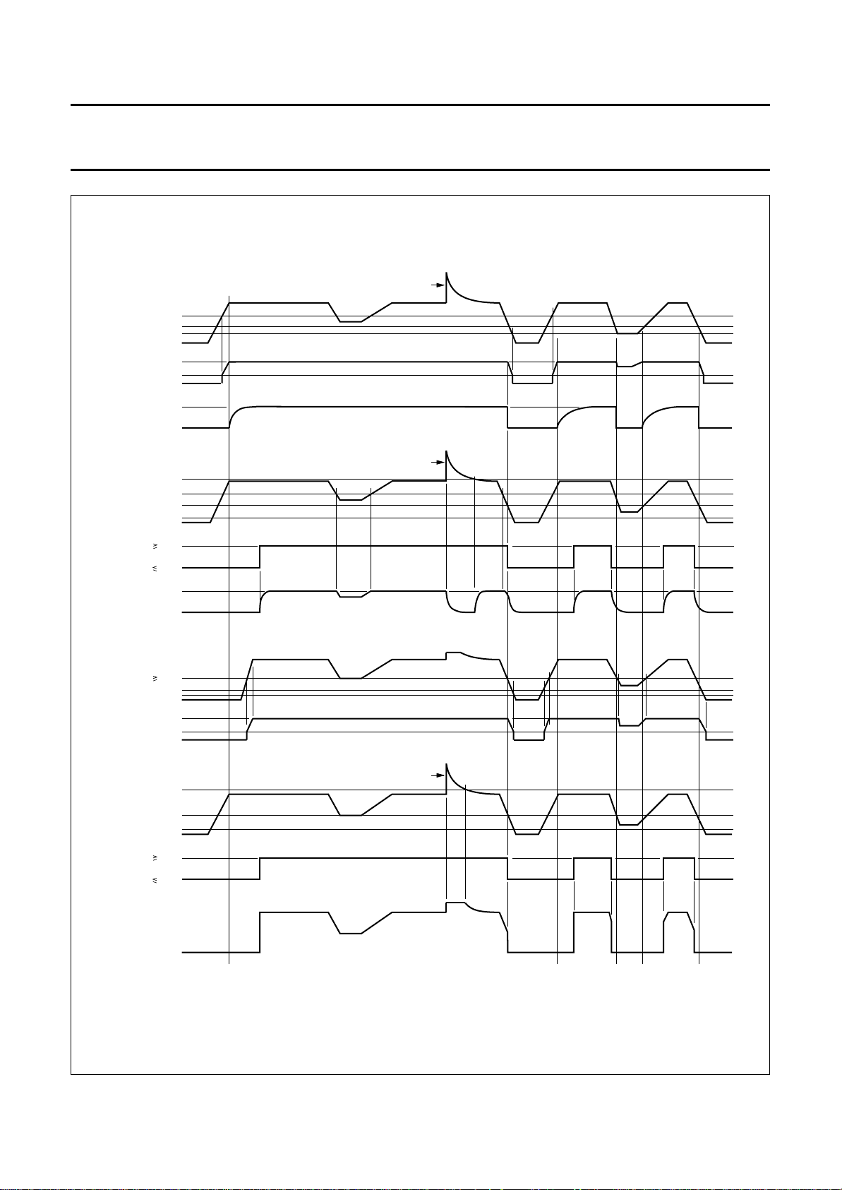
The total timing of a semi on/off logic set is shown Fig.4.
≤ 18 V).
P
1995 Oct 04 6
Page 7
Philips Semiconductors Preliminary specification
Multiple voltage regulator with switch TDA3603
handbook, full pagewidth
V
P
regulator 2
reset
18.0 V
V
P
enable
regulator 1
regulator 1
ignition
input
ignition
output
6.5 V
5.4 V
4.0 V
5.0 V
1.9 V
0 V
5.0 V
0 V
8.9 V
4.5 V
4.0 V
2.2 V
2.0 V
8.5 V
0 V
5.4 V
2.2 V
2.0 V
5.0 V
0.2 V
load dump
load dump
16.9 V
V
P
4.5 V
4.0 V
2.2 V
enable
power
switch
2.0 V
power
switch
output
0 V
1995 Oct 04 7
load dump
MBE235
Fig.4 Timing diagram.
Page 8
Philips Semiconductors Preliminary specification
Multiple voltage regulator with switch TDA3603
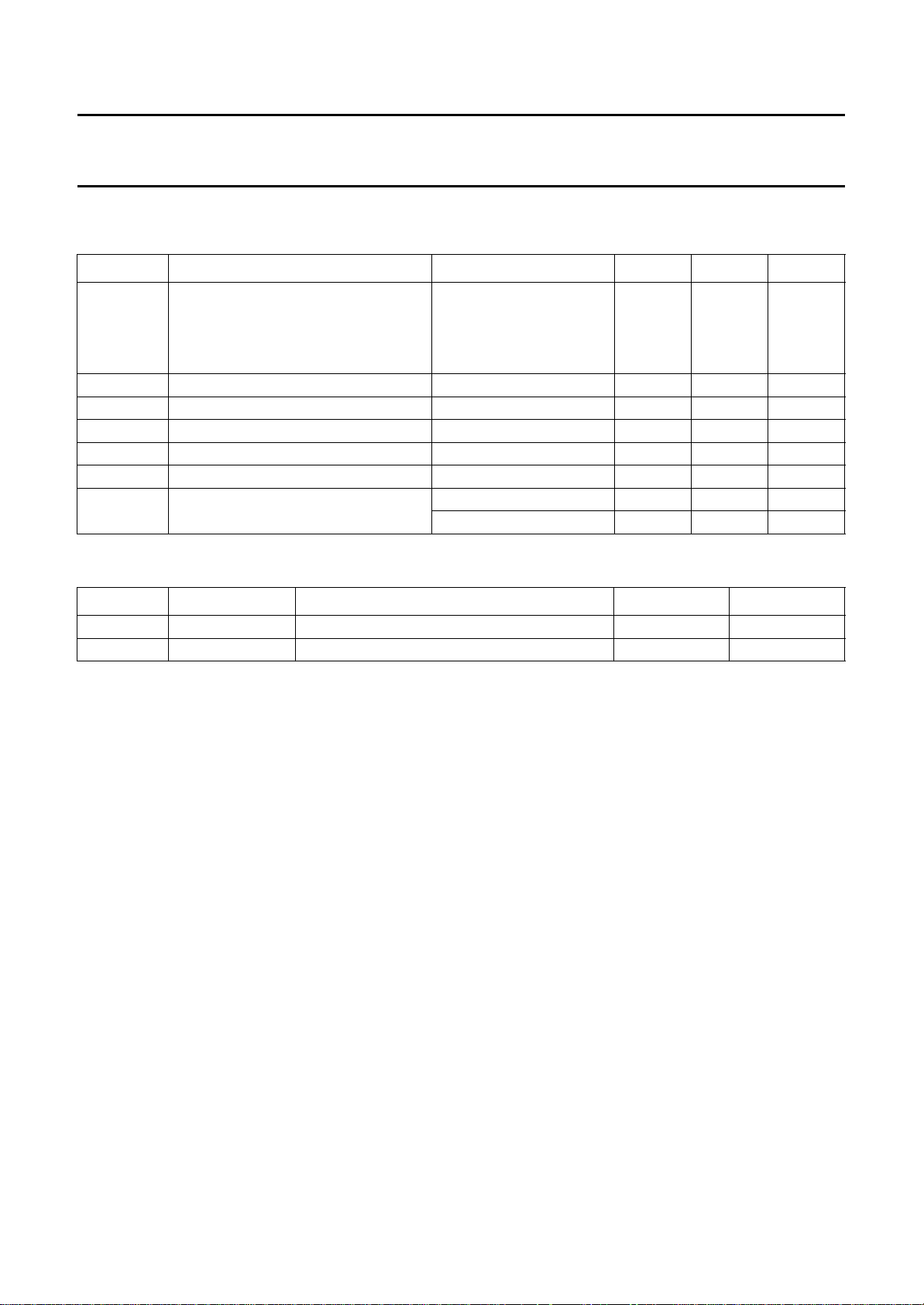
LIMITING VALUES
In accordance with the Absolute Maximum Rating System (IEC 134).
SYMBOL PARAMETER CONDITIONS MIN. MAX. UNIT
V
P
V
P
V
ppi
V
npi
T
stg
T
vj
P
tot
supply voltage
operating − 25 V
jump start t ≤ 10 minutes − 30 V
load dump protection during 50 ms; t
≥ 2.5 ms − 50 V
r
reverse battery voltage non-operating −−18 V
positive pulse voltage at ignition buffer VP= 14.4; RI=1kΩ− 50 V
negative pulse voltage at ignition buffer VP= 14.4; RI=1kΩ− −100 V
storage temperature non-operating −55 +150 °C
operating virtual junction temperature −40 +150 °C
total power dissipation SOT110-1 − 10.4 W
SOT398-1 − tbf W
THERMAL CHARACTERISTICS
SYMBOL TYPE NUMBER PARAMETER VALUE UNIT
R
R
th j-c
th j-p
TDA3603 thermal resistance from junction to case 12 K/W
TDA3603P thermal resistance from junction to pins 15 K/W
1995 Oct 04 8
Page 9
Philips Semiconductors Preliminary specification
Multiple voltage regulator with switch TDA3603
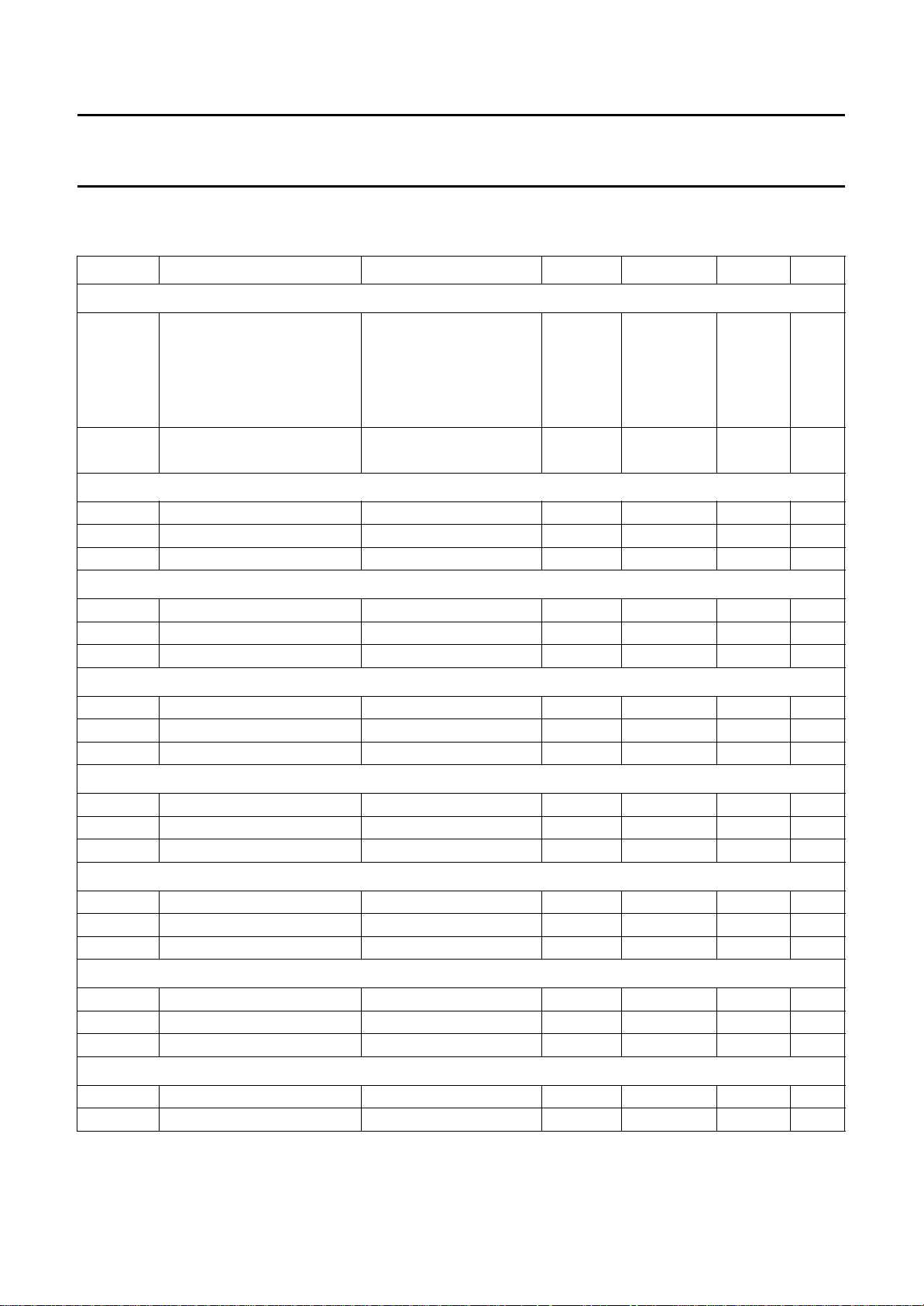
CHARACTERISTICS
V
= 14.4 V; Tamb = 25 °C; see Figs 5 and 6; unless otherwise specified.
P
SYMBOL PARAMETER CONDITIONS MIN. TYP. MAX. UNIT
Supply
V
P
I
q
Schmitt-trigger power supply for the power switch
V
thr
V
thf
V
hys
Schmitt-trigger power supply for regulator 1
V
thr
V
thf
V
hys
Schmitt-trigger power supply for regulator 2
V
thr
V
thf
V
hys
Schmitt-trigger for enable input
V
thr
V
thf
V
hys
Schmitt-trigger for reset buffer
V
r(REG2)
V
f(REG2)
V
spread
Schmitt-trigger for ignition buffer
V
thr
V
thf
V
hys
Reset buffer
I
sink
I
leak
supply voltage
operating 9.75 14.4 25 V
regulator 2 on note 1 2.4 14.4 25 V
jump start t ≤ 10 minutes −− 30 V
load dump protection during 50 ms; t
≥ 2.5 ms −− 50 V
r
quiescent current VP= 12.4 V; note 2 − 400 500 µA
= 14.4 V; note 2 − 420 −µA
V
P
rising voltage threshold 4.0 4.5 5.0 V
falling voltage threshold 3.5 4.0 4.5 V
hysteresis − 0.5 − V
rising voltage threshold 4.0 4.5 5.0 V
falling voltage threshold 3.5 4.0 4.5 V
hysteresis − 0.5 − V
rising voltage threshold 6.0 6.5 7.1 V
falling voltage threshold 1.7 1.9 2.2 V
hysteresis − 4.7 − V
rising voltage threshold 1.7 2.2 2.7 V
falling voltage threshold 1.5 2.0 2.5 V
hysteresis − 0.2 − V
rising voltage of regulator 2 note 3 − V
falling voltage of regulator 2 note 3 − V
− 0.15 − V
REG2
− 0.25 − V
REG2
voltage spread on tracking note 4 − 10 − mV
rising voltage threshold 1.7 2.2 2.7 V
falling voltage threshold 1.5 2.0 2.5 V
hysteresis − 0.2 − V
LOW-level sink current V
leakage current VP= 14.4 V; V
≤ 0.8 V 15 20 − mA
RES
= 5 V 25 50 100 µA
RES
1995 Oct 04 9
Page 10
Philips Semiconductors Preliminary specification
Multiple voltage regulator with switch TDA3603
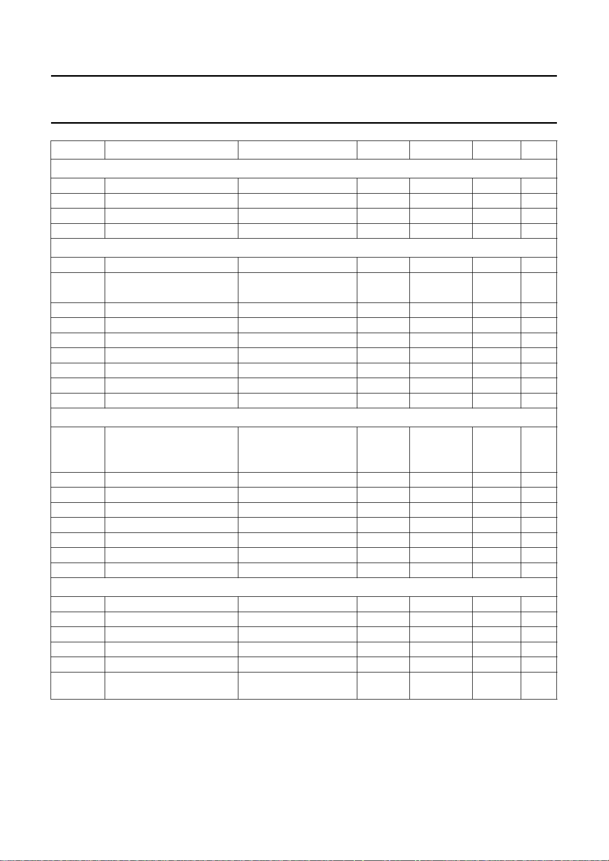
SYMBOL PARAMETER CONDITIONS MIN. TYP. MAX. UNIT
Ignition buffer
V
OL
V
OH
I
OL
I
OH
Regulator 1 (note 6)
V
REG1
V
REG1
∆V
REG1
∆V
REGL1
SVRR1 supply voltage ripple rejection f
V
REGd1
I
REGm1
I
REGsc1
α
ct
Regulator 2 (note 11)
V
REG2
∆V
REG2
∆V
REGL2
SVRR2 supply voltage ripple rejection f
V
REGd2
I
REGm2
I
REGsc2
α
ct
Power switch
V
swd
I
swcc
V
swcl
I
M
V
swfb
I
lim(sw)
LOW-level output voltage IOL= 0 mA 0 0.2 0.8 V
HIGH-level output voltage note 5 − 5.0 5.2 V
LOW-level output current VOL≤ 0.8 V 0.3 0.8 − mA
HIGH-level output current VOH≥ 3 V 0.3 2.0 − mA
output voltage off − 1 400 mV
output voltage 0.5 mA ≤ I
10 V ≤ V
≤ 300 mA 8.65 9.0 9.35 V
REG1
≤ 18 V 8.65 9.0 9.35 V
P
line regulation 10 V ≤ VP≤ 18 V −− 50 mV
load regulation 0.5 mA ≤ I
= 200 Hz; VI= 2 V (p-p) 60 −−dB
i
drop-out voltage I
current limit V
= 300 mA; note 7 − 0.4 0.5 V
REG1
> 7 V; note 8 0.45 - 1.2 A
REG1
≤ 300 mA −− 70 mV
REG1
short-circuit current RL≤ 0.5 Ω; note 9 50 300 − mA
cross talk note 10 − 50 − dB
output voltage 0.5 mA ≤ I
7V≤V
P
18 V ≤ V
≤ 30 mA 4.8 5.0 5.2 V
REG2
≤18 V 4.8 5.0 5.2 V
≤ 50 V 4.75 5.0 5.25 V
P
line regulation 7 V ≤ VP≤ 18 V −− 50 mV
load regulation 0.5 mA ≤ I
= 200 Hz; VI= 2 V (p-p) 60 −−dB
i
drop-out voltage I
current limit V
= 30 mA; note 12 − 0.3 0.4 V
REG2
> 4.5 V; note 8 0.1 - 0.5 A
REG2
≤ 30 mA −− 50 mV
REG1
short-circuit current RL≤ 0.5 Ω; note 9 − 50 − mA
cross talk note 13 − 50 − dB
drop-out voltage Isw= 0.3 A; note 14 − 0.4 0.9 V
continuous current 0.5 −−A
clamping voltage VP≥ 16.9 V − 15.0 16.2 V
peak current t ≤ 10 ms 1.4 −−A
fly back voltage behaviour Isw= −200 mA −− 20 V
current limit VP= 14.4 V; Vsw=10V;
0.6 − 1.0 A
note 8
1995 Oct 04 10
Page 11

Philips Semiconductors Preliminary specification
Multiple voltage regulator with switch TDA3603
Notes to the characteristics
1. Minimum operating voltage, only if VP has exceeded 6.5 V.
2. Enable and ignition inputs are low and regulator 2 is unloaded.
3. Voltage drop due to load condition.
4. The spread on tracking is one sigma value.
5. Ignition output voltage will be less than or equal to the output voltage of regulator 2.
6. I
7. The drop-out voltage of regulator 1 is measured between VP and V
8. At current limit, I
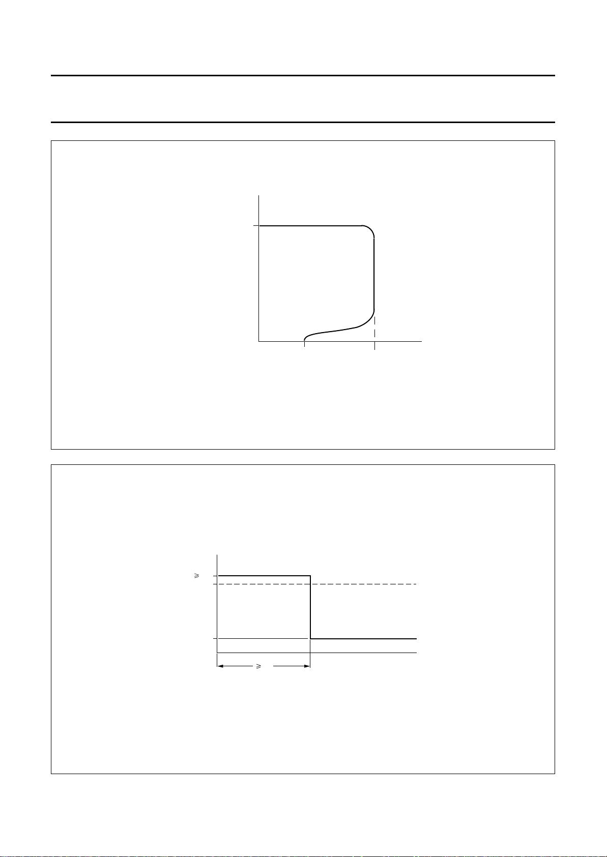
9. The foldback current protection limits the dissipated power at short-circuit (see Figs 5 and 6).
10. The cross talk of regulator 1 is measured with an I
11. I
12. The drop-out voltage of regulator 2 is measured between VP and V
13. The cross talk of regulator 2 is measured with an I
14. The drop-out voltage of the power switch is measured between VP and Vsw.
= 5 mA.
REG1
= 5 mA.
REG2
fi= 100 kHz.
.
REG1
is held constant (behaviour in accordance with the broken line in Fig.5).
REGm
= 0.5 mA up to 30 mA with an input frequency of fi= 100 kHz.
REG2
.
REG2
= 0.5 mA up to 100 mA with an input frequency of
REG1
1995 Oct 04 11
Page 12
Philips Semiconductors Preliminary specification
Multiple voltage regulator with switch TDA3603
handbook, halfpage
Rx
V
(regulators 1 and 2)
0
V
0
I
sc
I
m
I (regulators 1 and 2)
o
Fig.5 Foldback current protection of the regulators.
MBE233
1995 Oct 04 12
handbook, halfpage
1.4
1.4
I
sw
(A)
0.5
10
MBE234
t (ms)
Fig.6 Foldback current protection of the power switch.
Page 13
Philips Semiconductors Preliminary specification
Multiple voltage regulator with switch TDA3603
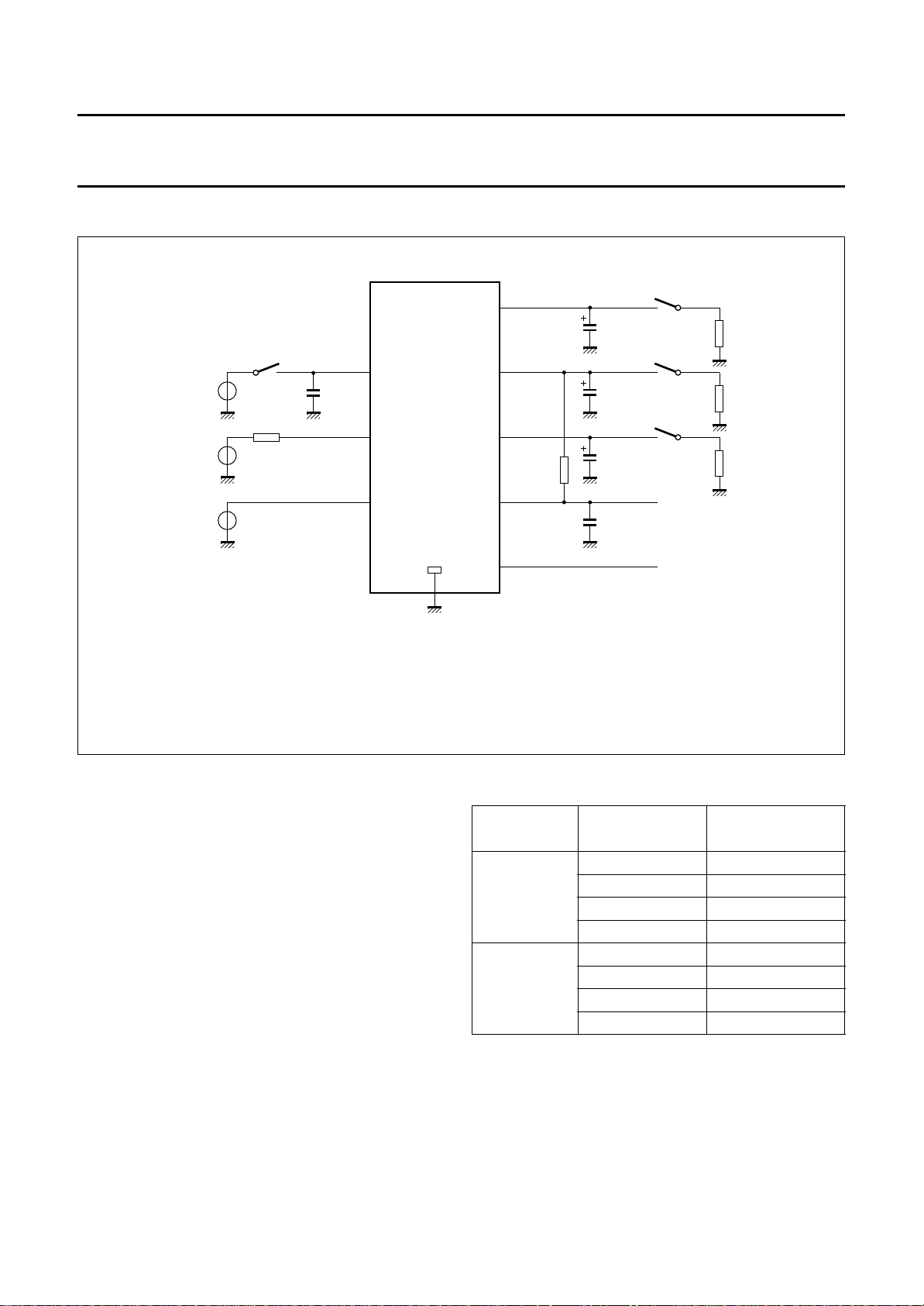
TEST AND APPLICATION INFORMATION
handbook, full pagewidth
V
P
V
en
V
I(ig)
(1) Capacitor not required for stability.
220 nF
R1
1 kΩ
(1)
C1
enable input
ignition input
V
sw
9
V
P
1
4
TDA3603
8
6
ground
regulator 2
7
regulator 1
2
reset
output
3
ignition
output
5
47 kΩ
R2
C2
10 µF
C3
10 µF
C4
10 µF
C5
1 µF
5 V
8.5 V
MBE232
R
L(sw)
1 kΩ
R
L(REG2)
1 kΩ
R
L(REG1)
1 kΩ
Fig.7 Test circuit.
Noise information
The noise at the output of the regulators depends on the
bandwidth of the regulators, which can be adjusted by the
output capacitors. Table 1 shows the noise figures.
Although stability is guaranteed when CL is higher than
10 µF (over temperature range) with tan (φ) = 1 in the
frequency range 1 to 10 kHz, however, for low noise, a
47 µF load capacitor is required.
The noise on the supply line depends on the value of the
supply capacitor and is caused by a current noise (output
noise of the regulators is translated into a current noise by
the output capacitors). When a high frequency capacitor of
220 nF with an electrolytic capacitor of 100 µF in parallel
is placed directly over pins 1 and 6 (supply and ground)
the noise is minimized.
1995 Oct 04 13
Table 1 Noise figures
REGULATOR NOISE (µV)
tbf 10
1
150 47
tbf 100
tbf 220
tbf 10
2
100 47
tbf 100
tbf 220
Note
1. Bandwidth of 100 kHz.
(1)
CAPACITOR (µF)
OUTPUT
Page 14
Philips Semiconductors Preliminary specification
Multiple voltage regulator with switch TDA3603
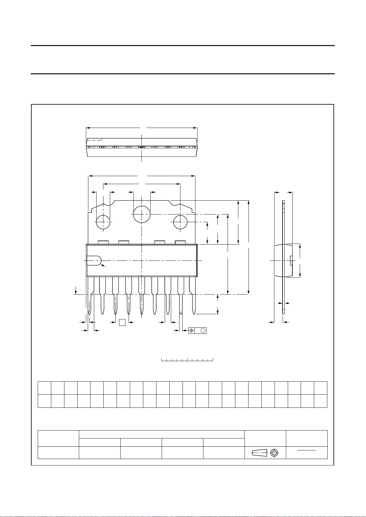
PACKAGE OUTLINES
SIL9MPF: plastic single in-line medium power package with fin; 9 leads
D
D
1
q
P
pin 1 index
P
1
q
2
q
1
SOT110-1
A
2
A
3
A
A
4
E
seating plane
19
Z
b
e
2
b
b
1
0 5 10 mm
scale
DIMENSIONS (mm are the original dimensions)
UNIT
mm
A
18.5
17.8
max.
3.7
2
A
8.7
8.0
A
3
4
15.8
15.4
b
0.67
0.50
b
1
2
1.40
1.14
bcD
1.40
1.14
0.48
0.38
21.8
21.4
(1)
D
1
21.4
20.7
A
Note
1. Plastic or metal protrusions of 0.25 mm maximum per side are not included.
OUTLINE
VERSION
IEC JEDEC EIAJ
REFERENCES
SOT110-1
w M
(1)
E
eLPP
6.48
6.20
2.54
3.9
3.4
L
c
Q
(1)
w
0.25
Z
max.
1.0
2.75
2.50
1
3.4
3.2
q
Q
1.75
15.1
1.55
14.9
EUROPEAN
PROJECTION
q1q
2
5.9
4.4
5.7
4.2
ISSUE DATE
92-11-17
95-02-25
1995 Oct 04 14
Page 15
Philips Semiconductors Preliminary specification
Multiple voltage regulator with switch TDA3603
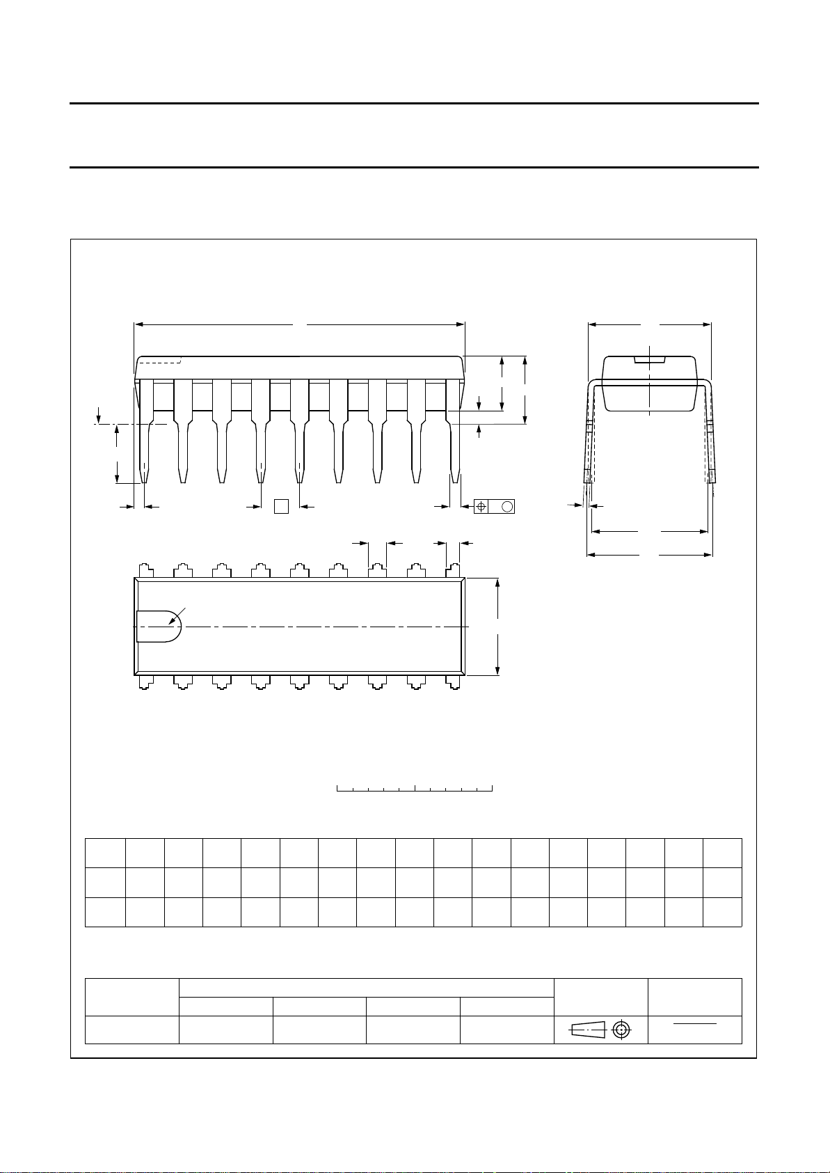
HDIP18: plastic heat-dissipating dual in-line package; 18 leads
D
seating plane
L
Z
18
pin 1 index
e
b
SOT398-1
M
E
A
2
A
A
1
b
w M
1
b
2
10
E
c
(e )
1
M
H
1
0 5 10 mm
scale
DIMENSIONS (inch dimensions are derived from the original mm dimensions)
A
A
A
UNIT
max.
mm
inches
Note
1. Plastic or metal protrusions of 0.25 mm maximum per side are not included.
OUTLINE
VERSION
SOT398-1
12
min.
max.
IEC JEDEC EIAJ
b
1.40
1.14
0.06
0.04
b
1
0.67
0.50
0.03
0.02
b
cD E e M
2
0.47
1.05
0.38
0.75
0.02
0.04
0.01
0.03
REFERENCES
21.85
21.35
0.87
0.84
1995 Oct 04 15
9
(1) (1)
6.5
6.2
0.26
0.24
L
e
1
M
3.9
8.32
3.1
8.02
0.15
0.33
0.12
0.32
EUROPEAN
PROJECTION
E
0.34
0.30
H
8.7
7.7
w
max.
0.252.54 7.62
0.010.10 0.30
0.040.19 0.02 0.15
ISSUE DATE
94-04-13
95-01-25
1.04.7 0.51 3.7
(1)
Z
Page 16

Philips Semiconductors Preliminary specification
Multiple voltage regulator with switch TDA3603
SOLDERING
Introduction
There is no soldering method that is ideal for all IC
packages. Wave soldering is often preferred when
through-hole and surface mounted components are mixed
on one printed-circuit board. However, wave soldering is
not always suitable for surface mounted ICs, or for
printed-circuits with high population densities. In these
situations reflow soldering is often used.
This text gives a very brief insight to a complex technology.
A more in-depth account of soldering ICs can be found in
our
“IC Package Databook”
Soldering by dipping or by wave
The maximum permissible temperature of the solder is
260 °C; solder at this temperature must not be in contact
DEFINITIONS
Data sheet status
Objective specification This data sheet contains target or goal specifications for product development.
Preliminary specification This data sheet contains preliminary data; supplementary data may be published later.
Product specification This data sheet contains final product specifications.
Limiting values
Limiting values given are in accordance with the Absolute Maximum Rating System (IEC 134). Stress above one or
more of the limiting values may cause permanent damage to the device. These are stress ratings only and operation
of the device at these or at any other conditions above those given in the Characteristics sections of the specification
is not implied. Exposure to limiting values for extended periods may affect device reliability.
Application information
Where application information is given, it is advisory and does not form part of the specification.
(order code 9398 652 90011).
with the joint for more than 5 seconds. The total contact
time of successive solder waves must not exceed
5 seconds.
The device may be mounted up to the seating plane, but
the temperature of the plastic body must not exceed the
specified maximum storage temperature (T
printed-circuit board has been pre-heated, forced cooling
may be necessary immediately after soldering to keep the
temperature within the permissible limit.
Repairing soldered joints
Apply a low voltage soldering iron (less than 24 V) to the
lead(s) of the package, below the seating plane or not
more than 2 mm above it. If the temperature of the
soldering iron bit is less than 300 °C it may remain in
contact for up to 10 seconds. If the bit temperature is
between 300 and 400 °C, contact may be up to 5 seconds.
stg max
). If the
LIFE SUPPORT APPLICATIONS
These products are not designed for use in life support appliances, devices, or systems where malfunction of these
products can reasonably be expected to result in personal injury. Philips customers using or selling these products for
use in such applications do so at their own risk and agree to fully indemnify Philips for any damages resulting from such
improper use or sale.
1995 Oct 04 16
Page 17

Philips Semiconductors Preliminary specification
Multiple voltage regulator with switch TDA3603
NOTES
1995 Oct 04 17
Page 18

Philips Semiconductors Preliminary specification
Multiple voltage regulator with switch TDA3603
NOTES
1995 Oct 04 18
Page 19

Philips Semiconductors Preliminary specification
Multiple voltage regulator with switch TDA3603
NOTES
1995 Oct 04 19
Page 20

Philips Semiconductors – a worldwide company
Argentina: IEROD, Av. Juramento 1992 - 14.b, (1428)
BUENOS AIRES, Tel. (541)786 7633, Fax. (541)786 9367
Australia: 34 Waterloo Road, NORTH RYDE, NSW 2113,
Tel. (02)805 4455, Fax. (02)805 4466
Austria: Triester Str. 64, A-1101 WIEN, P.O. Box 213,
Tel. (01)60 101-1236, Fax. (01)60 101-1211
Belgium: Postbus 90050, 5600 PB EINDHOVEN, The Netherlands,
Tel. (31)40-2783749, Fax. (31)40-2788399
Brazil: Rua do Rocio 220 - 5
CEP: 04552-903-SÃO PAULO-SP, Brazil.
P.O. Box 7383 (01064-970),
Tel. (011)821-2333, Fax. (011)829-1849
Canada: PHILIPS SEMICONDUCTORS/COMPONENTS:
Tel. (800) 234-7381, Fax. (708) 296-8556
Chile: Av. Santa Maria 0760, SANTIAGO,
Tel. (02)773 816, Fax. (02)777 6730
China/Hong Kong: 501 Hong Kong Industrial Technology Centre,
72 Tat Chee Avenue, Kowloon Tong, HONG KONG,
Tel. (852)2319 7888, Fax. (852)2319 7700
Colombia: IPRELENSO LTDA, Carrera 21 No. 56-17,
77621 BOGOTA, Tel. (571)249 7624/(571)217 4609,
Fax. (571)217 4549
Denmark: Prags Boulevard 80, PB 1919, DK-2300
COPENHAGEN S, Tel. (032)88 2636, Fax. (031)57 1949
Finland: Sinikalliontie 3, FIN-02630 ESPOO,
Tel. (358)0-615 800, Fax. (358)0-61580 920
France: 4 Rue du Port-aux-Vins, BP317,
92156 SURESNES Cedex,
Tel. (01)4099 6161, Fax. (01)4099 6427
Germany: P.O. Box 10 63 23, 20043 HAMBURG,
Tel. (040)3296-0, Fax. (040)3296 213.
Greece: No. 15, 25th March Street, GR 17778 TAVROS,
Tel. (01)4894 339/4894 911, Fax. (01)4814 240
India: Philips INDIA Ltd, Shivsagar Estate, A Block,
Dr. Annie Besant Rd. Worli, Bombay 400 018
Tel. (022)4938 541, Fax. (022)4938 722
Indonesia: Philips House, Jalan H.R. Rasuna Said Kav. 3-4,
P.O. Box 4252, JAKARTA 12950,
Tel. (021)5201 122, Fax. (021)5205 189
Ireland: Newstead, Clonskeagh, DUBLIN 14,
Tel. (01)7640 000, Fax. (01)7640 200
Italy: PHILIPS SEMICONDUCTORS S.r.l.,
Piazza IV Novembre 3, 20124 MILANO,
Tel. (0039)2 6752 2531, Fax. (0039)2 6752 2557
Japan: Philips Bldg 13-37, Kohnan 2-chome, Minato-ku, TOKYO 108,
Tel. (03)3740 5130, Fax. (03)3740 5077
Korea: Philips House, 260-199 Itaewon-dong,
Yongsan-ku, SEOUL, Tel. (02)709-1412, Fax. (02)709-1415
Malaysia: No. 76 Jalan Universiti, 46200 PETALING JAYA,
SELANGOR, Tel. (03)750 5214, Fax. (03)757 4880
Mexico: 5900 Gateway East, Suite 200, EL PASO, TX 79905,
Tel. 9-5(800)234-7381, Fax. (708)296-8556
th
floor, Suite 51,
Netherlands: Postbus 90050, 5600 PB EINDHOVEN, Bldg. VB,
Tel. (040)2783749, Fax. (040)2788399
New Zealand: 2 Wagener Place, C.P.O. Box 1041, AUCKLAND,
Tel. (09)849-4160, Fax. (09)849-7811
Norway: Box 1, Manglerud 0612, OSLO,
Tel. (022)74 8000, Fax. (022)74 8341
Pakistan: Philips Electrical Industries of Pakistan Ltd.,
Exchange Bldg. ST-2/A, Block 9, KDA Scheme 5, Clifton,
KARACHI 75600, Tel. (021)587 4641-49,
Fax. (021)577035/5874546
Philippines: PHILIPS SEMICONDUCTORS PHILIPPINES Inc,
106 Valero St. Salcedo Village, P.O. Box 2108 MCC, MAKATI,
Metro MANILA, Tel. (63) 2 816 6380, Fax. (63) 2 817 3474
Portugal: PHILIPS PORTUGUESA, S.A.,
Rua dr. António Loureiro Borges 5, Arquiparque - Miraflores,
Apartado 300, 2795 LINDA-A-VELHA,
Tel. (01)4163160/4163333, Fax. (01)4163174/4163366
Singapore: Lorong 1, Toa Payoh, SINGAPORE 1231,
Tel. (65)350 2000, Fax. (65)251 6500
South Africa: S.A. PHILIPS Pty Ltd.,
195-215 Main Road Martindale, 2092 JOHANNESBURG,
P.O. Box 7430, Johannesburg 2000,
Tel. (011)470-5911, Fax. (011)470-5494
Spain: Balmes 22, 08007 BARCELONA,
Tel. (03)301 6312, Fax. (03)301 42 43
Sweden: Kottbygatan 7, Akalla. S-164 85 STOCKHOLM,
Tel. (0)8-632 2000, Fax. (0)8-632 2745
Switzerland: Allmendstrasse 140, CH-8027 ZÜRICH,
Tel. (01)488 2211, Fax. (01)481 77 30
Taiwan: PHILIPS TAIWAN Ltd., 23-30F, 66, Chung Hsiao West
Road, Sec. 1. Taipeh, Taiwan ROC, P.O. Box 22978,
TAIPEI 100, Tel. (886) 2 382 4443, Fax. (886) 2 382 4444
Thailand: PHILIPS ELECTRONICS (THAILAND) Ltd.,
209/2 Sanpavuth-Bangna Road Prakanong,
Bangkok 10260, THAILAND,
Tel. (66) 2 745-4090, Fax. (66) 2 398-0793
Turkey:Talatpasa Cad. No. 5, 80640 GÜLTEPE/ISTANBUL,
Tel. (0212)279 27 70, Fax. (0212)282 67 07
United Kingdom: Philips Semiconductors LTD.,
276 Bath Road, Hayes, MIDDLESEX UB3 5BX,
Tel. (0181)730-5000, Fax. (0181)754-8421
United States:811 East Arques Avenue, SUNNYVALE,
CA 94088-3409, Tel. (800)234-7381, Fax. (708)296-8556
Uruguay: Coronel Mora 433, MONTEVIDEO,
Tel. (02)70-4044, Fax. (02)92 0601
Internet: http://www.semiconductors.philips.com/ps/
For all other countries apply to: Philips Semiconductors,
International Marketing and Sales, Building BE-p,
P.O. Box 218, 5600 MD EINDHOVEN, The Netherlands,
Telex 35000 phtcnl, Fax. +31-40-2724825
SCD44 © Philips Electronics N.V. 1995
All rights are reserved. Reproduction in whole or in part is prohibited without the
prior written consent of the copyright owner.
The information presented in this document does not form part of any quotation
or contract, is believed to be accurate and reliable and may be changed without
notice. No liability will be accepted by the publisher for any consequence of its
use. Publication thereof does not convey nor imply any license under patent- or
other industrial or intellectual property rights.
Printed in The Netherlands
513061/1500/02/pp20 Date of release: 1995 Oct 04
Document order number: 9397 750 00342
 Loading...