

Page 1

INTEGRATED CIRCUITS
DATA SH EET
TDA3566
PAL/NTSC decoder
Preliminary specification
File under Integrated Circuits, IC02
May 1989
Page 2

Philips Semiconductors Preliminary specification
PAL/NTSC decoder TDA3566
GENERAL DESCRIPTION
The TDA3566 is a monolithic integrated decoder for the PAL and/or NTSC colour television standards. It combines all
functions required for the identification and demodulation of PAL/NTSC signals. Furthermore it contains a luminance
amplifier, an RGB-matrix and amplifier. These amplifiers supply output signals up to 4 V peak-to-peak (picture
information) enabling direct drive of the discrete output stages. The circuit also contains separate inputs for data
insertion, analogue as well as digital, which can be used for text display systems (e.g. Teletext/broadcast antiope),
channel number display, etc.
Features
• A black-current stabilizer which controls the black-currents of the three electron-guns to a level low enough to omit the
black-level adjustment
• Contrast control of inserted RGB signals
• No black-level disturbance when non-synchronized external RGB signals are available on the inputs
• NTSC capability with hue control
QUICK REFERENCE DATA
Supply voltage (pin 1) V
Supply current (pin 1) I
P=V1-27
= I
P
1
typ. 12 V
typ. 80 mA
Luminance amplifier (pin 8)
Input voltage (peak-to-peak value) V
8-27(p-p)
typ. 450 mV
Contrast control range typ. 20 dB
Chrominance amplifier (pin 4)
Input voltage range (peak-to-peak value) V
4-27(p-p)
40 to 1100 mV
Saturation control range min. 50 dB
RGB matrix and amplifiers
Output voltage at nominal luminance and contrast
(peak-to-peak value) V
13, 15, 17-27(p-p)
typ. 4 V
Data insertion
Input signals (peak-to-peak value) V
12, 14, 16-27(p-p)
typ. 1 V
Data blanking (pin 9)
Input voltage for data insertion V
9-27
min. 0,9 V
Sandcastle input (pin 7)
Blanking input voltage V
Burst gating and clamping input voltage V
7-27
7-27
typ. 1,5 V
typ. 7 V
PACKAGE OUTLINE
28-lead DIL; plastic, with internal heat spreader (SOT117); SOT117-1, 1996 November 21.
May 1989 2
Page 3
Philips Semiconductors Preliminary specification
PAL/NTSC decoder TDA3566
May 1989 3
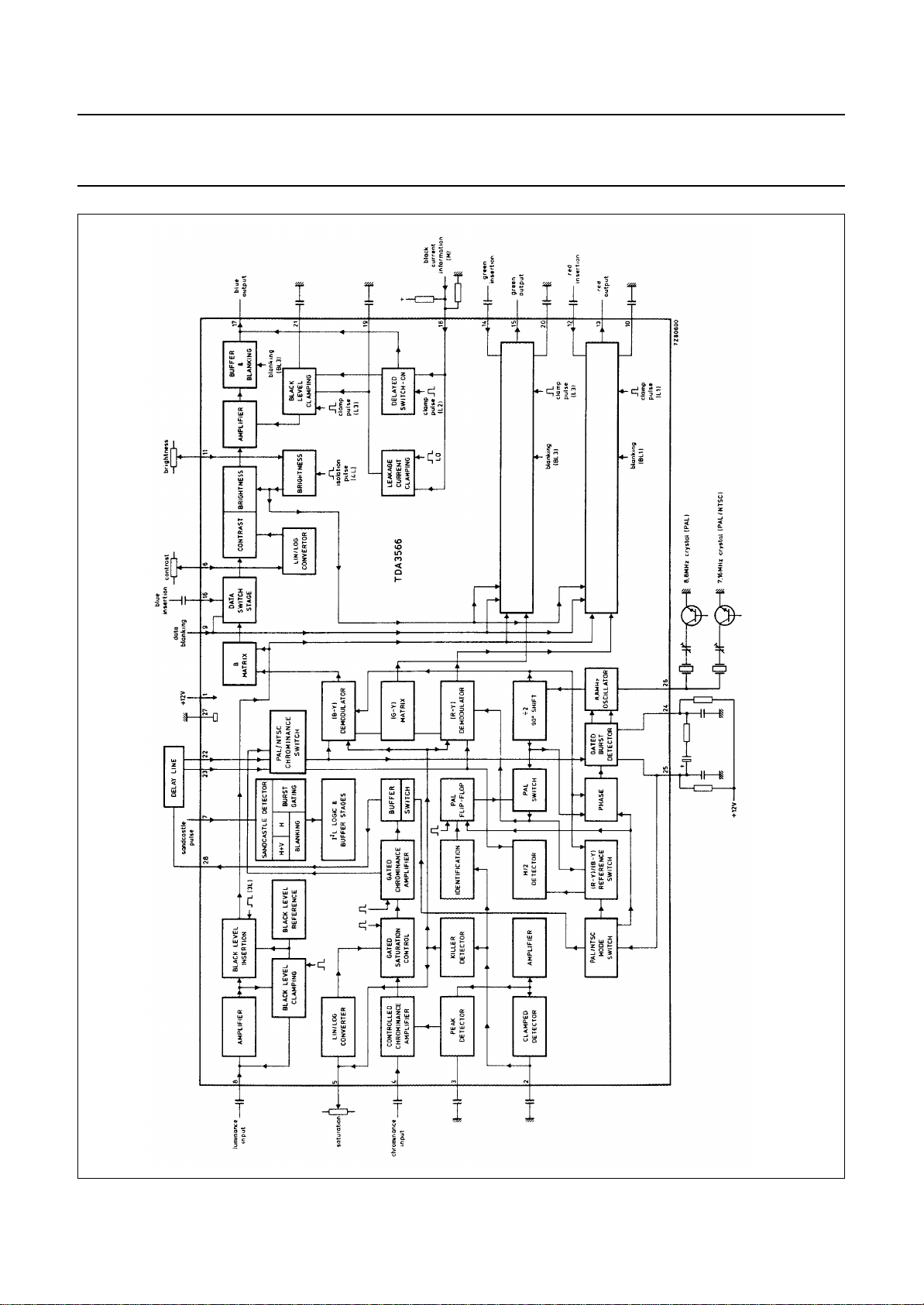
Fig.1 Block diagram; for explanation of pulse mnemonics see Fig.6.
Page 4

Philips Semiconductors Preliminary specification
PAL/NTSC decoder TDA3566
FUNCTIONAL DESCRIPTION
The TDA3566 is a further development of the TDA3562A. It has the same pinning and almost the same application.
The differences between the TDA3562A and the TDA3566 are as follows:
• The NTSC-application has largely been simplified. In the case of NTSC the chroma signal is now internally coupled to
the demodulators, ACC and phase detectors. The chroma output signal (pin 28) is suppressed in this case. It follows
that the external switches and filters which are needed for the TDA3562A are not needed for the TDA3566.
Furthermore there is no difference between the amplitude of the colour output signals in the PAL or NTSC mode. The
PAL/NTSC-switch and the hue control of the TDA3566 and the TDA3562A are identical.
• The switch-on and the switch-off behaviour of the TDA3566 has been improved. This has been obtained by
suppressing the output signals during the switch-on and switch-off periods.
• The clamp capacitors connected to the pins 10, 20 and 21 can be reduced to 100 nF for the TDA3566. The clamp
capacitors also receive a pre-bias voltage to avoid coloured background during switch-on.
• The crystal oscillator circuit has been changed to prevent parasitic oscillations on the third overtone of the crystal. This
has the consequence that optimal tuning capacitance must be reduced to 10 pF.
Luminance amplifier
The luminance amplifier is voltage driven and requires an input signal of 450 mV peak-to-peak (positive video). The
luminance delay line must be connected between the i.f. amplifier and the decoder. The input signal is a.c. coupled to
the input (pin 8). After amplification, the black level at the output of the preamplifier is clamped to a fixed d.c. level by the
black level clamping circuit. During three line periods after vertical blanking, the luminance signal is blanked out and the
black level reference voltage is inserted by a switching circuit. This black level reference voltage is controlled via pin 11
(brightness). At the same time the RGB signals are clamped. Noise and residual signals have no influence during
clamping thus simple internal clamping circuitry is used.
Chrominance amplifiers
The chrominance amplifier has an asymmetrical input. The input signal must be a.c. coupled (pin 4) and have a minimum
amplitude of 40 mV peak-to-peak. The gain control stage has a control range in excess of 30 dB, the maximum input
signal must not exceed 1,1 V peak-to-peak, otherwise clipping of the input signal will occur. From the gain control stage
the chrominance signal is fed to the saturation control stage. Saturation is linear controlled via pin 5. The control voltage
range is 2 to 4 V, the input impedance is high and the saturation control range is in excess of 50 dB. The burst signal is
not affected by saturation control. The signal is then fed to a gated amplifier which has a 12 dB higher gain during the
chrominance signal. As a result the signal at the output (pin 28) has a burst to chrominance ratio which is 6 dB lower than
that of the input signal when the saturation control is set at −6 dB. The chrominance output signal is fed to the delay line
and, after matrixing, is applied to the demodulator input pins (pins 22 and 23). These signals are fed to the burst phase
detector. In the case of NTSC the chroma signal is internally coupled to the demodulators, ACC and phase detector.
Oscillator and identification circuit
The burst phase detector is gated with the narrow part of the sandcastle pulse (pin 7). In the detector the (R-Y) and (B-Y)
signals are added to provide the composite burst signal again. This composite signal is compared with the oscillator
signal divided-by-2 ((R-Y) reference signal). The control voltage is available at pins 24 and 25, and is also applied to the
8,8 MHz oscillator. The 4,4 MHz signal is obtained via the divide-by-2 circuit, which generates both the (B-Y) and (R-Y)
reference signals and provides a 90° phase shift between them.
The flip-flop is driven by pulses obtained from the sandcastle detector. For the identification of the phase at PAL mode,
the (R-Y) reference signal coming from the PAL switch, is compared to the vertical signal (R-Y) of the PAL delay line.
This is carried out in the H/2 detector, which is gated during burst. When the phase is incorrect, the flip-flop gets a reset
from the identification circuit. When the phase is correct, the output voltage of the H/2 detector is directly related to the
burst amplitude so that this voltage can be used for the a.c.c. To avoid ‘blooming-up’ of the picture under weak input
signal conditions the a.c.c. voltage is generated by peak detection of the H/2 detector output signal.
May 1989 4
Page 5

Philips Semiconductors Preliminary specification
PAL/NTSC decoder TDA3566
The killer and identification circuits get their information from a gated output signal of the H/2 detector. Killing is obtained
via the saturation control stage and the demodulators to obtain good suppression. The time constant of the saturation
control (pin 5) provides a delayed switch-on after killing.
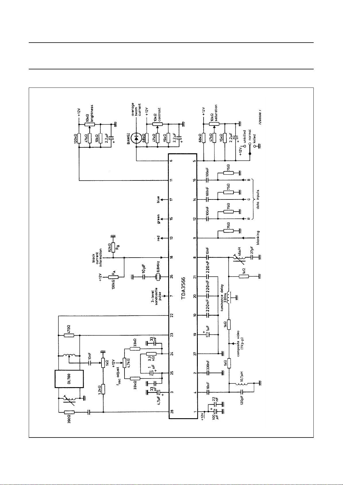
Adjustment of the oscillator is achieved by variation of the burst phase detector load resistance between pins 24 and 25
(see Fig.7). With this application the trimmer capacitor in series with the 8,8 MHz crystal (pin 26) can be replaced by a
fixed value capacitor to compensate for unbalance of the phase detector.
Demodulator
The (R-Y) and (B-Y) demodulators are driven by the colour difference signals from the delay-line matrix circuit and the
reference signals from the 8,8 MHz divider circuit. The (R-Y) reference signal is fed via the PAL-switch. The output
signals are fed to the R and B matrix circuits and to the (G-Y) matrix to provide the (G-Y) signal which is applied to the
G-matrix. The demodulation circuits are killed and blanked by by-passing the input signals.
NTSC mode
The NTSC mode is switched on when the voltage at the burst phase detector outputs (pins 24 and 25) is adjusted below
9 V. To ensure reliable application the phase detector load resistors are external. When the TDA3566 is used only for
PAL these two 33 kΩ resistors must be connected to +12 V (see Fig.7). For PAL/NTSC application the value of each
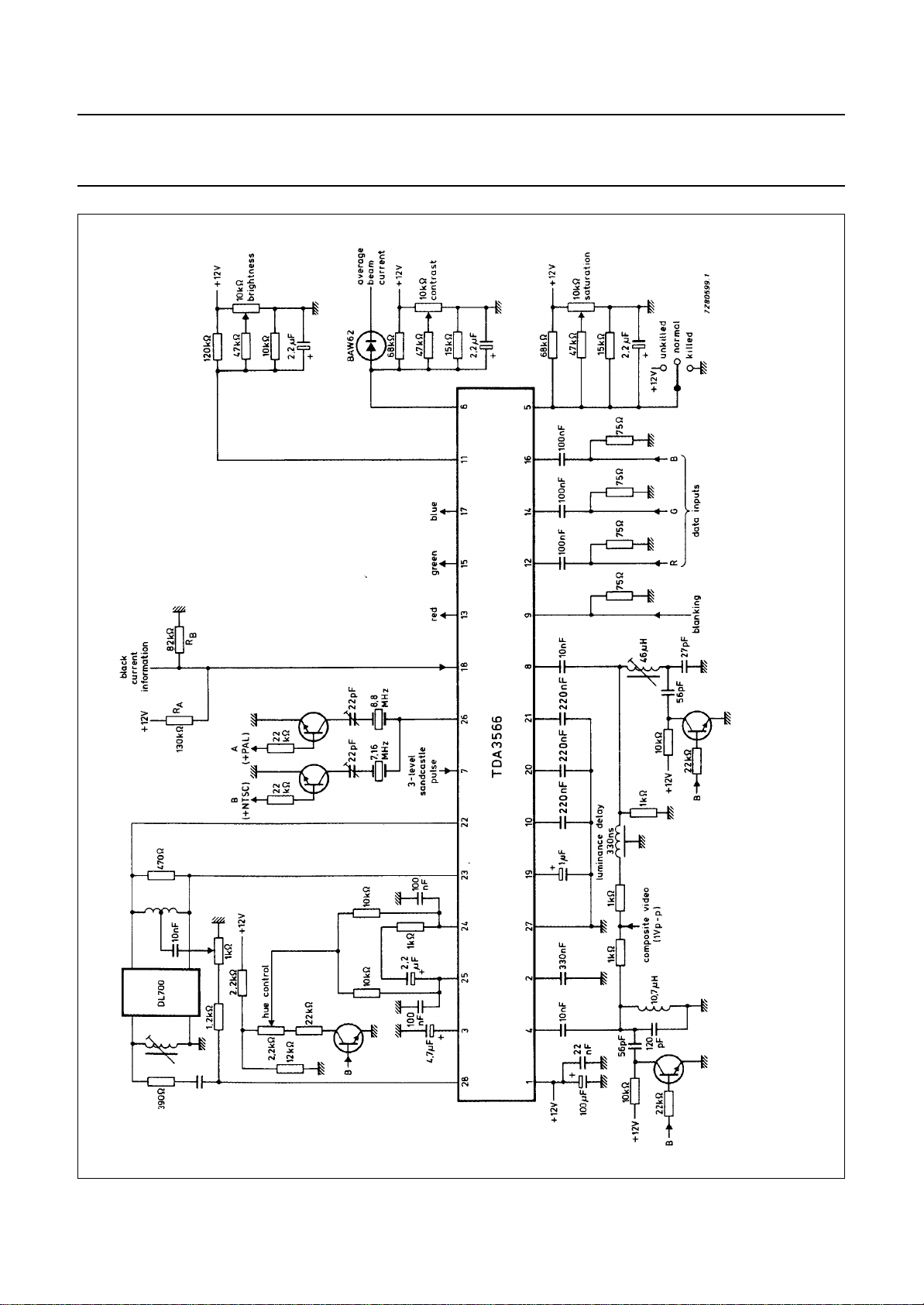
resistor must be reduced to 10 kΩ and connected to the slider of a potentiometer (see Fig.8). The switching transistor
brings the voltage at pins 24 and 25 below 9 V which switches the circuit to the NTSC mode. The position of the PAL
flip-flop ensures that the correct phase of the (R-Y) reference signal is supplied to the (R-Y) demodulator. The drive to
the H/2 detector is now provided by the (B-Y) reference signal. (In the PAL mode it is driven by the (R-Y) reference
signal.)
Hue control is realized by changing the phase of the reference drive to the burst phase detector. This is achieved by
varying the voltage at pins 24 and 25 between 7,5 V and 8,5 V, nominal position 8,0 V. The hue control characteristic is
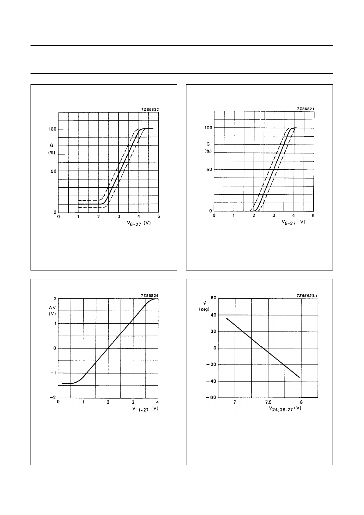
shown in Fig.5.
RGB matrix and amplifiers
The three matrix and amplifier circuits are identical and only one circuit will be described. The luminance and the colour
difference signals are added in the matrix circuit to obtain the colour signal, which is then fed to the contrast control stage.
The contrast control voltage is supplied to pin 6 (high-input impedance). The control range is + 3 db to−17 dB nominal.
The relationship between the control voltage and the gain is linear (see Fig.2).
During the 3-line period after blanking a pulse is inserted at the output of the contrast control stage. The amplitude of this
pulse is varied by a control voltage at pin 11. This applies a variable offset to the normal black level, thus providing
brightness control. The brightness control range is 1 V to 3 V.
While this offset level is present, the ‘black-current’ input impedance (pin 18) is high and the internal clamp circuit is
activated. The clamp circuit then compares the reference voltage at pin 19 with the voltage developed across the external
resistor network R
stored in capacitors connected from pins 10, 20 and 21 to ground which controls the black level at the output. The
reference voltage is composed by the resistor divider network and the leakage current of the picture tube into this
bleeder. During vertical blanking, this voltage is stored in the capacitor connected to pin 19, which ensures that the
leakage current of the CRT does not influence the black current measurement.
The RGB output signals can never exceed a level of 10 V. When the signal tends to exceed this level the output signal
is clipped. The black level at the outputs (pins 13, 15 and 17) will be about 3 V. This level depends on the spread of the
guns of the picture tube. If a beam current stabilizer is not used it is possible to stabilize the black levels at the outputs,
which in this application must be connected to the black current measuring input (pin 18) via a resistor network.
and RB (pin 18) which is provided by picture tube beam current. The output of the comparator is
A
May 1989 5
Page 6

Philips Semiconductors Preliminary specification
PAL/NTSC decoder TDA3566
Data insertion
Each colour amplifier has a separate input for data insertion. A 1 V peak-to-peak input signal provides a 4 V peak-to-peak
output signal. To avoid the ‘black-level’ of the inserted signal differing from the black level of the normal video signal, the
data is clamped to the black level of the luminance signal. Therefore a.c. coupling is required for the data inputs.
To avoid a disturbance of the blanking level due to the clamping circuit, the source impedance of the driver circuit must
not exceed 150 Ω.
The data insertion circuit is activated by the data blanking input (pin 9). When the voltage at this pin exceeds a level of
0,9 V, the RGB matrix circuits are switched off and the data amplifiers are switched on. To avoid coloured edges, the
data blanking switching time is short.
The amplitude of the data output signals is controlled by the contrast control at pin 6. The black level is equal to the video
black level and can be varied between 2 and 4 V (nominal condition) by the brightness control voltage at pin 11.
Non-synchronized data signals do not disturb the black level of the internal signals.
Blanking of RGB and data signals
Both the RGB and data signals can be blanked via the sandcastle input (pin 7). A slicing level of 1,5 V is used for this
blanking function, so that the wide part of the sandcastle pulse is separated from the remainder of the pulse. During
blanking a level of + 1 V is available at the output.
To prevent parasitic oscillations on the third overtone of the crystal the optimal tuning capacitance should be 10 pF.
RATINGS
Limiting values in accordance with Absolute Maximum System (IEC 134)
Supply voltage (pin 1) V
Total power dissipation P
Storage temperature range T
Operating ambient temperature range T
THERMAL RESISTANCE
From junction to ambient (in free air) R
= V
P
tot
stg
amb
th j-a
1-27
max. 13,2 V
max. 1,7 W
−25 to + 150 °C
−25 to + 70 °C
= 40 K/W
May 1989 6
Page 7

Philips Semiconductors Preliminary specification
PAL/NTSC decoder TDA3566
CHARACTERISTICS
= V
V
P
Supply (pin 1)
Supply voltage V
Supply current I
Total power dissipation P
Luminance amplifier (pin 8)
Input voltage (note 2)
Input level before clipping V
Input current I
Contrast control range (see Fig.2) −15 −+5dB
Input current contrast control I
Chrominance amplifier (pin 4)
Input voltage note 3
Input impedance (pin 4) Z
Input capacitance C
A.C.C. control range 30 −−dB
Change of the burst signal at the output
Gain at nominal contrast/saturation
Chrominance to burst ratio
Maximum output voltage range
Distortion of chrominance amplifier
Frequency response between 0 and 5 MHz α
Saturation control range (see Fig.3) 50 −−dB
Input current saturation control (pin 5) I
Cross-coupling between luminance
Signal-to-noise ratio
= 12 V; T
1-27
= 25 °C; unless otherwise specified
amb
PARAMETER SYMBOL MIN. TYP. MAX. UNIT
(peak-to-peak value) V
(peak-to-peak value) V
= V
P
1-27
= I
P
1
tot
8-27(p-p)
8-27
8
7
4-27(p-p)
− 10 − kΩ
4-27
4-27
10,8 12 13,2 V
− 80 110 mA
− 0,95 1,3 W
− 0,45 0,63 V
−− 1.4 V
− 0,1 1 µA
−− 15 µA
40 390 1100 mV
−− 6,5 pF
over the whole control range ∆V −− 1dB
pin 4 to pin 28. (note 4) G 34 −−dB
at nominal saturation (notes 3 and 4)
− 12 − dB
at pin 28.
(peak-to-peak value); R
at V
28-27(p-p)
up to V
= 2 V (output)
4-27(p-p)
= 1 V (input)
= 2 kΩ V
L
28-27(p-p)
d −− 5%
28-4
5
45 −V
−− −2dB
−− 20 µA
and chrominance amplifier (note 5) −− −46 dB
at nominal input signal (note 6) S/N 56 −−dB
May 1989 7
Page 8

Philips Semiconductors Preliminary specification
PAL/NTSC decoder TDA3566
PARAMETER SYMBOL MIN. TYP. MAX. UNIT
Phase shift between burst and chrominance
at nominal contrast/saturation ∆ϕ − − ± 5 deg
Output impedance of chrominance amplifier Z
Output current I
Reference part
Phase-locked-loop
catching range (note 7) ∆f 500 700 − Hz
phase shift for ± 400 Hz deviation
(note 7) ∆ϕ − − 5 deg
of f
osc
Oscillator
temperature coefficient of oscillator
frequency (note 7) TC
frequency variation when supply voltage
increases from 10 to 13,2 V (note 7) ∆f
input resistance (pin 26) R
input capacitance (pin 26) C
A.C.C. generation (pin 2)
control voltage at nominal input signal V
control voltage without chrominance input V
colour-off voltage V
colour-on voltage V
identification-on voltage V
change in burst amplitude with temperature − 0,1 0,25 %/K
voltage at pin 3 at nominal input signal V
Demodulator part
Input burst signal amplitude
(peak-to-peak value)
between pins 23 and 27 (note 8)
Input impedance
between pins 22 or 23 and 27 Z
Ratio of demodulated signals (note 9)
(B-Y)/(R-Y)
− 10 −Ω
28-27
28
osc
osc
26-27
26-27
2-27
2-27
2-27
2-27
2-27
3-27
V
23-27(p-p)
22-27/23-27
V
17 27–
-----------------V
13 27–
−− 15 mA
−−2 −3 Hz/K
− 40 100 Hz
280 400 520 Ω
−− 10 pF
− 4,5 − V
− 2 − V
− 2,8 − V
− 3 − V
− 1,7 − V
− 5,1 − V
68 80 95 mV
0,7 1 1,3 kΩ
− 1,78 ± 10% −
(G-Y)/(R-Y); no (B-Y) signal
(G-Y)/(B-Y); no (R-Y) signal
May 1989 8
V
15 27–
-----------------V
13 27–
V
15 27–
-----------------V
17 27–
−−0,51 ± 10% −
−−0,19 ± 10% −
Page 9

Philips Semiconductors Preliminary specification
PAL/NTSC decoder TDA3566
PARAMETER SYMBOL MIN. TYP. MAX. UNIT
Frequency response between 0 and 1 MHz α
17
Cross-talk between colour difference signals 40 −−dB
Phase difference between (R-Y) signal
and (R-Y) reference signals ∆ϕ − − 5 deg
Phase difference between (R-Y) signal
and (B-Y) reference signals ∆ϕ 85 90 95 deg
RGB matrix and amplifiers
Output voltage (peak-to-peak value)
at nominal luminance/contrast
V
13,15,17-27(p-p)
(black-to-white) (note 4)
Output voltage at pin 13
(peak-to-peak value)
V
13-27(p-p)
at nominal contrast/saturation and no luminance
signal to (R-Y)
Maximum peak-white level V
13,15,17 (m)
Available output current
(pins 13, 15, 17) I
13,15,17
Difference between black level and
measuring level at the output for
∆V
13,15,17-27
a brightness control voltage at pin 11
of 2 V (note 10)
Difference in black level between the three
channels without black current
∆V −− 100 mV
stabilization (note 11)
Control range of black-current
stabilization at V
= 3 V; V
b1
= 2 V −− ±2V
11-17
Black level shift with vision contents ∆V −− 40 mV
Brightness control voltage range see Fig.4
Brightness control input current I
11
Variation of black level with temperature ∆V/∆T − 0 − mV/K
Variation of black level with contrast (note 1) ∆V −− 100 mV
Relative spread between the
R, G and B output signals −− 10 %
Relative black-level variation between the
three channels during variation of
∆V − 020mV
contrast, brightness and supply voltage
(± 10%) (note 1)
Differential black-level drift over a
temperature range of 40 °C ∆V − 020mV
Blanking level at the RGB outputs V
bl
−− −3dB
3,5 4 4,5 V
− 4,2 − V
9,7 10 10,3 V
10 −−mA
− 0 − V
−− 5µA
− 0,95 1,1 V
May 1989 9
Page 10

Philips Semiconductors Preliminary specification
PAL/NTSC decoder TDA3566
PARAMETER SYMBOL MIN. TYP. MAX. UNIT
Difference in blanking level of the
three channels V
bl
Differential drift of the blanking levels
over a temperature range of 40 °CV
Tracking of output black level with supply voltage 0,9 1 1,1
bl
Vbl∆
----------V
V
P
×
---------V
∆
bl
Tracking of contrast control between
the three channels over a control range at 10 dB −− 0,5 dB
Output signal during the clamp pulse
(3L) after switch-on V
O
Signal-to-noise ratio of output signals
(note 6) S/N 62 −−dB
Residual 4,4 MHz signal at RGB outputs
(peak-to-peak value) V
R(p-p)
Residual 8,8 MHz signal and higher
harmonics at the RGB outputs
V
R(p-p)
(peak-to-peak value)
Output impedance of RGB outputs Z
13,15,17-27
Frequency response of total luminance
and RGB amplifier circuits for f = 0 to 9 MHz α−−1−3dB
Current source of output stage I
O
Difference of black level at the three
outputs at nominal brightness (note 1) ∆V −− 10 mV
Tracking of brightness control −− 2%
− 0 − mV
− 010mV
P
7,5 −−V
−− 50 mV
−− 150 mV
− 50 −Ω
23 −mA
Signal insertion (pins 12, 14 and 16)
Input signals (peak-to-peak value) for
and RGB output voltage of 3.5 V
V
12,14,16-27(p-p)
(peak-to-peak) at nominal contrast
Difference between the black levels
of the RGB signals and the inserted
∆V −− 100 mV
signals at the output (note 12)
Output rise time t
r
Differential delay time
for the three channels t
Input current I
d
12,14,16
May 1989 10
0,9 1 1,1 V
− 50 80 ns
− 040ns
−− 10 µA
Page 11

Philips Semiconductors Preliminary specification
PAL/NTSC decoder TDA3566
PARAMETER SYMBOL MIN. TYP. MAX. UNIT
Data blanking (pin 9)
Input voltage for no data insertion V
Input voltage for data insertion V
Maximum input voltage V
Delay of data blanking t
Input resistance R
9-27
9-27
9-27(m)
d
9-27
Suppression of the internal RGB
signals when V
> 0,9 V 46 −−dB
9-27
Sandcastle input (pin 7)
Level at which the RGB blanking
is activated V
7-27
Level at which the horizontal pulses
are separated V
7-27
Level at which burst gating and
clamping pulse are separated V
7-27
Delay between black level clamping
and burst gating pulse t
d
Input current
at V
at V
at V
= 0 to 1 V −I
7-27
= 1 to 8,5 V I
7-27
= 8,5 to 12 V I
7-27
7
7
7
Black current stabilization (pin 18)
Bias voltage (d.c.) V
18-27
Difference between input voltage for
“black” current and leakage current ∆V 0,35 0,5 0,65 V
Input current during ‘black’ current I
Input current during scan I
Internal limiting at pin 10 V
18
18
18-27
Switching threshold for
‘black’ current control ON V
Input resistance during scan R
18-27
18-27
Input current during scan
at pins 10, 20 and 21 (d.c.) I
10, 20, 21
Maximum charge/discharge current
during measuring time − 1 − nA
−− 0,4 V
0,9 −−V
−− 3V
−− 20 ns
710 13kΩ
1 1,5 2 V
3 3,5 4 V
6,5 7,0 7,5 V
− 0,6 −µs
−− 1mA
−− 50 µA
−− 2mA
3,5 5 7,0 V
−− 1µA
−− 10 mA
8,5 9 9,5 V
7,6 8 8,4 V
1 1,5 2 kΩ
−− tbf nA
NTSC
Level at which the PAL/NTSC switch is
activated (pins 24 and 25) V
Average output current (note 13) I
Hue control see Fig.5
May 1989 11
24-25
24 + 25(AV)
− 8,8 9,2 V
75 90 105 µA
Page 12

Philips Semiconductors Preliminary specification
PAL/NTSC decoder TDA3566
Notes to the characteristics
1. With respect to the measuring pulses.
2. Signal with the negative-going sync; amplitude includes sync amplitude.
3. Indicated is a signal for a colour bar with 75% saturation; chrominance to burst ratio is 2,2 : 1.
4. Nominal contrast is specified as the maximum contrast −5 dB and nominal saturation as the maximum
saturation −6 dB.
5. Cross coupling is measured under the following condition: input signal nominal, contrast and saturation such that
nominal output signals are obtained. The signals at the output at which no signal should be available must be
compared with the nominal output signal at that output.
6. The signal-to-noise ratio is defined as peak-to-peak signal with respect to r.m.s. noise.
7. All frequency variations are referred to 4,4 MHz carrier frequency.
8. These signal amplitudes are determined by the a.c.c. circuit of the reference part.
9. The demodulators are driven by a chrominance signal of equal amplitude for the (R-Y) and the (B-Y) components.
The phase of the (R-Y) chrominance signal equals the phase of the (R-Y) reference signal. This also applies to the
(B-Y) signals.
10. This value depends on the gain setting of the RGB output amplifiers and the drift of the picture tube guns. Higher
black level values are possible (up to 5 V) but in that application the amplitude of the output signal is reduced.
11. The variation of the black-level during brightness control in the three different channels is directly dependent on the
gain of each channel. Discolouration during adjustments of contrast and brightness does not occur because
amplitude and the black-level change with brightness control are directly related.
12. This difference occurs when the source impedance of the data signals is 150 Ω and the black level clamp pulse width
is 4 µs (sandcastle pulse). For a lower impedance the difference will be lower.
13. The voltage at pins 24 and 25 can be changed by connecting the load resistors (10 kΩ in this application) to the
slider bar of the hue control potentiometer (see Fig.8). When the transistor is switched on, the voltage at pins 24 and
25 is reduced below 9 V, and the circuit is switched to NTSC mode. The width of the burst gate is assumed to be
4 µs typical.
May 1989 12
Page 13
Philips Semiconductors Preliminary specification
PAL/NTSC decoder TDA3566
Fig.2 Contrast control voltage range. Fig.3 Saturation control voltage range.
Fig.4 Difference between black level and
measuring level at the RGB outputs (∆V) as
a function of the brightness control input
voltage (V
). Fig.5 Hue control voltage range.
11-27
May 1989 13
Page 14
Philips Semiconductors Preliminary specification
PAL/NTSC decoder TDA3566
May 1989 14
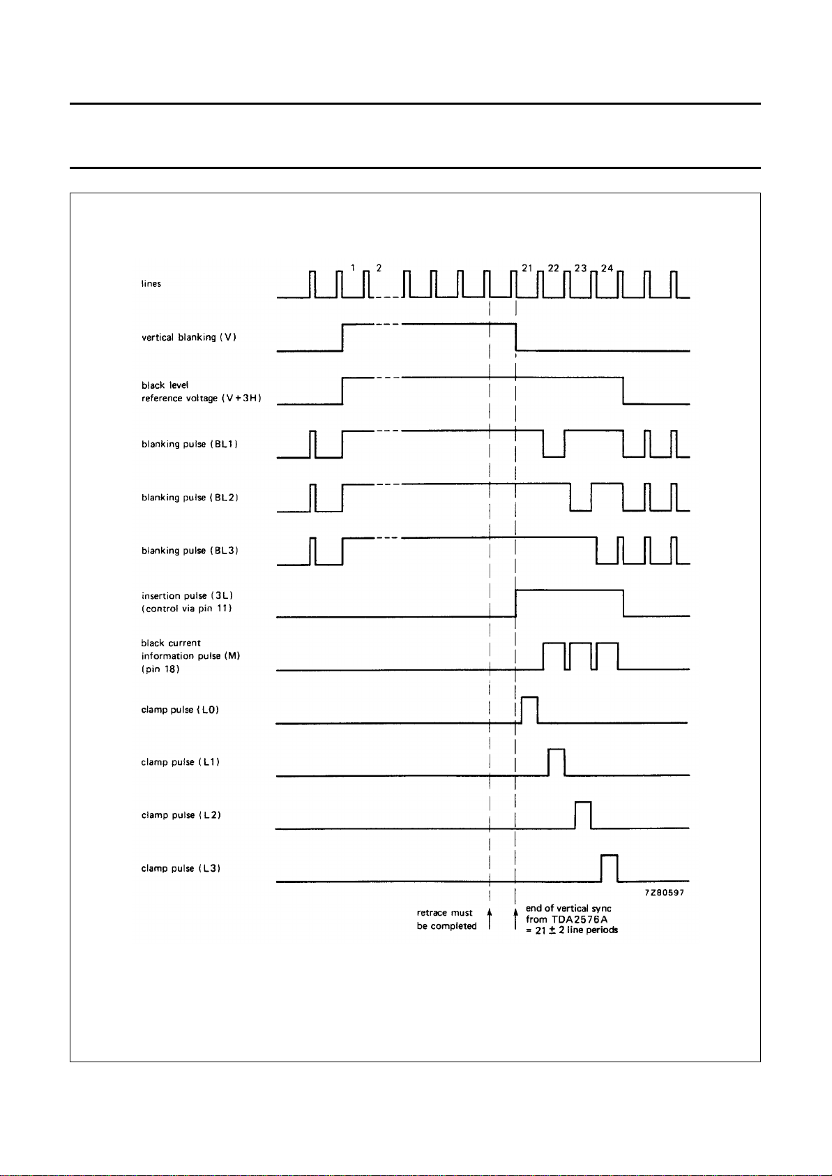
Fig.6 Timing diagram for black-current stabilizing.
Page 15
Philips Semiconductors Preliminary specification
PAL/NTSC decoder TDA3566
APPLICATION INFORMATION
May 1989 15
Fig.7 Application diagram showing the TDA3566 for a PAL decoder.
Page 16
Philips Semiconductors Preliminary specification
PAL/NTSC decoder TDA3566
May 1989 16
Fig.8 Application diagram showing the TDA3566 for a PAL/NTSC decoder.
Page 17
Philips Semiconductors Preliminary specification
PAL/NTSC decoder TDA3566
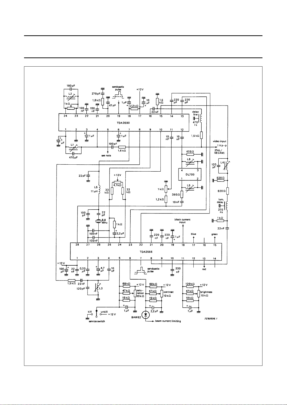
Note to pin 5 TDA3590:
V
< 1 V; horizontal identification and black level clamping.
5-2
> 11 V; vertical identification and artificial black level.
V
5-2
= 5 to 7 V; horizontal identification and artificial black level.
V
5-2
Fig.9 PAL/SECAM application circuit diagram using the TDA3590 and TDA3566.
May 1989 17
Page 18
Philips Semiconductors Preliminary specification
PAL/NTSC decoder TDA3566
PACKAGE OUTLINE
handbook, full pagewidth
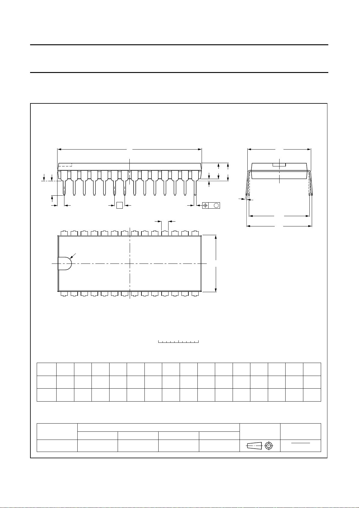
DIP28: plastic dual in-line package; 28 leads (600 mil)
SOT117-1
seating plane
L
Z
28
1
pin 1 index
D
A
2
A
A
1
e
b
w M
b
1
15
E
14
c
M
(e )
M
E
1
H
DIMENSIONS (inch dimensions are derived from the original mm dimensions)
A
UNIT
inches
Note
1. Plastic or metal protrusions of 0.25 mm maximum per side are not included.
max.
mm
OUTLINE
VERSION
SOT117-1
A
min.
May 1989 18
0 5 10 mm
A
1 2
max.
1.7
1.3
0.066
0.051
IEC JEDEC EIAJ
051G05 MO-015AH
b
b
0.53
0.38
0.020
0.014
cD E weM
1
0.32
0.23
0.013
0.009
REFERENCES
scale
(1) (1)
36.0
35.0
1.41
1.34
14.1
13.7
0.56
0.54
(1)
92-11-17
95-01-14
Z
max.
1.75.1 0.51 4.0
0.0670.20 0.020 0.16
L
3.9
3.4
EUROPEAN
PROJECTION
M
15.80
15.24
0.62
0.60
H
E
17.15
15.90
0.68
0.63
0.252.54 15.24
0.010.10 0.60
ISSUE DATE
e
1
0.15
0.13
Page 19

Philips Semiconductors Preliminary specification
PAL/NTSC decoder TDA3566
SOLDERING
Introduction
There is no soldering method that is ideal for all IC
packages. Wave soldering is often preferred when
through-hole and surface mounted components are mixed
on one printed-circuit board. However, wave soldering is
not always suitable for surface mounted ICs, or for
printed-circuits with high population densities. In these
situations reflow soldering is often used.
This text gives a very brief insight to a complex technology.
A more in-depth account of soldering ICs can be found in
“IC Package Databook”
our
Soldering by dipping or by wave
The maximum permissible temperature of the solder is
260 °C; solder at this temperature must not be in contact
DEFINITIONS
Data sheet status
Objective specification This data sheet contains target or goal specifications for product development.
Preliminary specification This data sheet contains preliminary data; supplementary data may be published later.
Product specification This data sheet contains final product specifications.
(order code 9398 652 90011).
with the joint for more than 5 seconds. The total contact
time of successive solder waves must not exceed
5 seconds.
The device may be mounted up to the seating plane, but
the temperature of the plastic body must not exceed the
specified maximum storage temperature (T
printed-circuit board has been pre-heated, forced cooling
may be necessary immediately after soldering to keep the
temperature within the permissible limit.
Repairing soldered joints
Apply a low voltage soldering iron (less than 24 V) to the
lead(s) of the package, below the seating plane or not
more than 2 mm above it. If the temperature of the
soldering iron bit is less than 300 °C it may remain in
contact for up to 10 seconds. If the bit temperature is
between 300 and 400 °C, contact may be up to 5 seconds.
stg max
). If the
Limiting values
Limiting values given are in accordance with the Absolute Maximum Rating System (IEC 134). Stress above one or
more of the limiting values may cause permanent damage to the device. These are stress ratings only and operation
of the device at these or at any other conditions above those given in the Characteristics sections of the specification
is not implied. Exposure to limiting values for extended periods may affect device reliability.
Application information
Where application information is given, it is advisory and does not form part of the specification.
LIFE SUPPORT APPLICATIONS
These products are not designed for use in life support appliances, devices, or systems where malfunction of these
products can reasonably be expected to result in personal injury. Philips customers using or selling these products for
use in such applications do so at their own risk and agree to fully indemnify Philips for any damages resulting from such
improper use or sale.
May 1989 19
 Loading...