

Page 1

INTEGRATED CIRCUITS
DATA SH EET
TDA2615
2 × 6 W hi-fi audio power amplifier
Product specification
Supersedes data of July 1994
File under Integrated Circuits, IC01
Philips Semiconductors
1995 May 08
Page 2

Philips Semiconductors Product specification
2 × 6 W hi-fi audio power amplifier TDA2615
FEATURES
• Requires very few external components
• No switch-on/switch-off clicks
• Input mute during switch-on and switch-off
GENERAL DESCRIPTION
The TDA2615 is a dual power amplifier in a 9-lead plastic
single-in-line (SIL9MPF) medium power package. It has
been especially designed for mains fed applications, such
as stereo radio and stereo TV.
• Low offset voltage between output and ground
• Excellent gain balance of both amplifiers
• Hi-fi in accordance with
“IEC 268”
and
“DIN 45500”
• Short-circuit proof and thermal protected
• Mute possibility.
QUICK REFERENCE DATA
Stereo application.
SYMBOL PARAMETER CONDITIONS MIN. TYP. MAX. UNIT
±V
P
P
O
G
v
channel unbalance − 0.2 − dB
G
v
supply voltage range 7.5 − 21 V
output power VS= ±12 V; THD = 0.5% − 6 − W
internal voltage gain − 30 − dB
α channel separation − 70 − dB
SVRR supply voltage ripple rejection − 60 − dB
V
no
noise output voltage − 70 −µV
ORDERING INFORMATION
TYPE
NUMBER
NAME DESCRIPTION VERSION
TDA2615 SIL9MPF
PACKAGE
plastic single in-line medium power package with fin; 9 leads
SOT110-1
1995 May 08 2
Page 3
Philips Semiconductors Product specification
2 × 6 W hi-fi audio power amplifier TDA2615
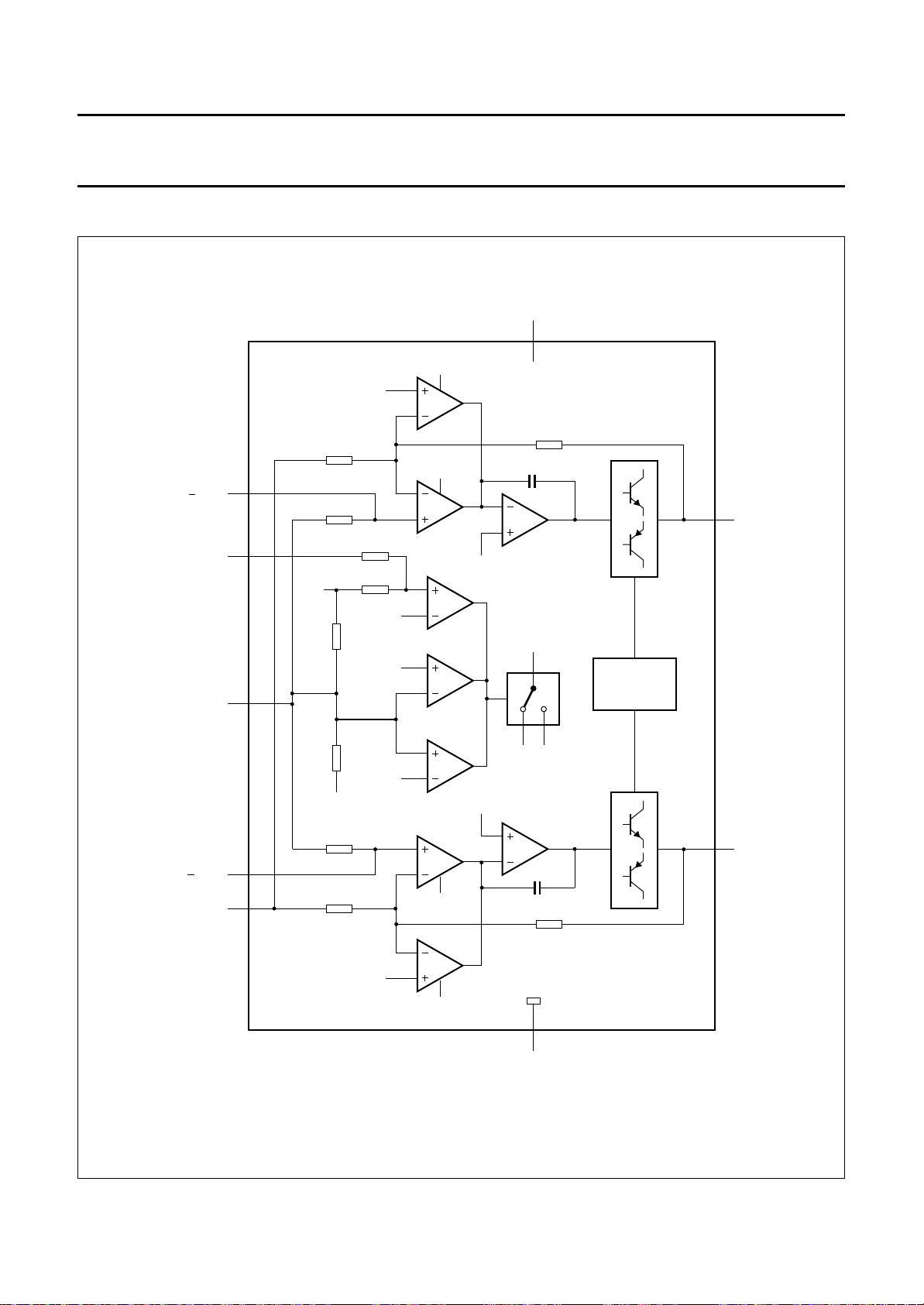
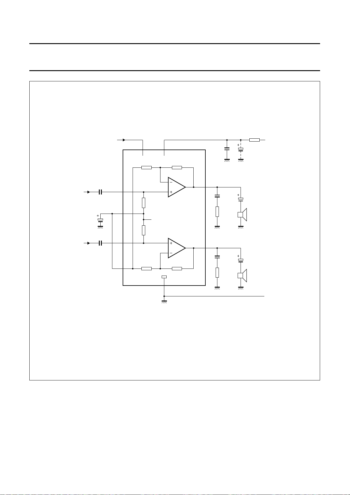
BLOCK DIAGRAM
+ V
P
INV1
MUTE
1/2 V / GND
P
V
A
V
ref1
680 Ω
V
1
20 kΩ
– V
10 kΩ
10 kΩ
P
4 kΩ
5 kΩ
+ V
– V
V
ref3
ref2
ref2
2
+ V
P
V
3
ref1
B
voltage
comparator
– V
– V
P
P
7
TDA2615
20 kΩ
CM
4
OUT1
+ V
P
THERMAL
PROTECTION
V
V
B
A
20 kΩ
INV2
INV1, 2
9
8
680 Ω
V
B
V
ref1
V
A
Fig.1 Block diagram.
1995 May 08 3
CM
– V
20 kΩ
5
P
MLA711
6
OUT2
Page 4
Philips Semiconductors Product specification
2 × 6 W hi-fi audio power amplifier TDA2615
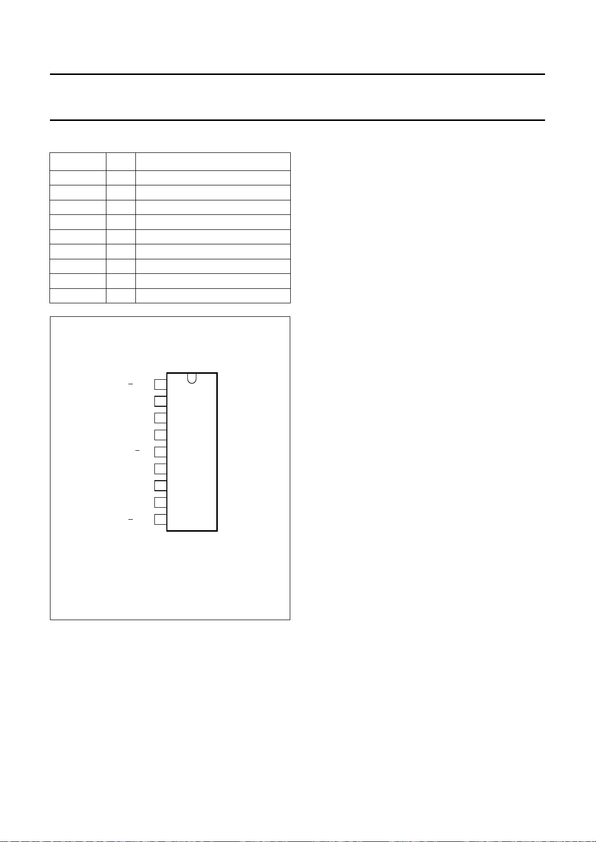
PINNING
SYMBOL PIN DESCRIPTION
−INV1 1 non-inverting input 1
MUTE 2 mute input
1
⁄2VP/GND 31⁄2 supply voltage or ground
OUT1 4 output 1
−V
P
5 supply voltage (negative)
OUT2 6 output 2
+V
P
7 supply voltage (positive)
INV1, 2 8 inverting input 1 and 2
−INV2 9 non-inverting input 2
INV1
1
MUTE
2
1/2 V
P
INV1, 2
/ GND
OUT1
V
OUT2
+ V
INV2
3
4
TDA2615
5
P
6
7
P
8
9
MLA708
FUNCTIONAL DESCRIPTION
The TDA2615 is a hi-fi stereo amplifier designed for mains
fed applications, such as stereo radio and stereo TV. The
circuit is optimally designed for symmetrical power
supplies, but is also well-suited to asymmetrical power
supply systems.
An output power of 2 × 6W (THD = 0.5%) can be
delivered into an 8 Ω load with a symmetrical power supply
of ±12 V. The gain is internally fixed at 30 dB, thus offering
a low gain spread and a very good gain balance between
the two amplifiers (0.2 dB).
A special feature is the input mute circuit. This circuit
disconnects the non-inverting inputs when the supply
voltage drops below±6 V, while the amplifier still retains its
DC operating adjustment. The circuit features suppression
of unwanted signals at the inputs, during switch-on and
switch-off.
The mute circuit can also be activated via pin 2. When a
current of 300 µA is present at pin 2, the circuit is in the
mute condition.
The device is provided with two thermal protection circuits.
One circuit measures the average temperature of the
crystal and the other measures the momentary
temperature of the power transistors. These control
circuits attack at temperatures in excess of +150 °C, so a
crystal operating temperature of max. +150 °C can be
used without extra distortion.
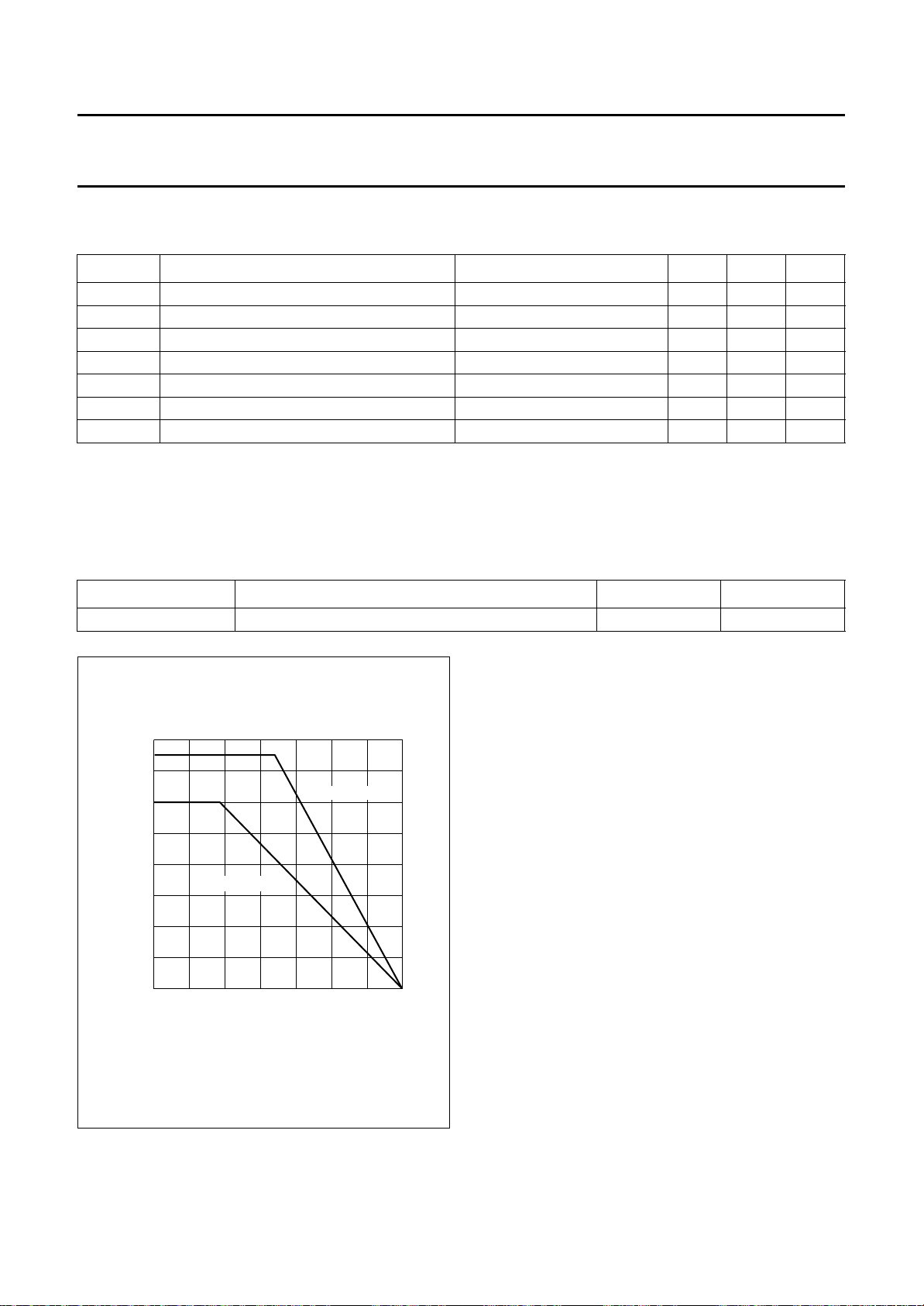
With the derating value of 6 K/W, the heatsink can be
calculated as follows:
=8Ω and VS= ±12 V, the measured maximum
at R
L
dissipation is 7.8 W.
Fig.2 Pin configuration.
1995 May 08 4
With a maximum ambient temperature of +60 °C, the
thermal resistance of the heatsink is:
150 60–
R
----------------------
th
7.8
6– 5.5 K/W==
The metal tab has the same potential as pin 5.
Page 5
Philips Semiconductors Product specification
2 × 6 W hi-fi audio power amplifier TDA2615
LIMITING VALUES
In accordance with the Absolute maximum System (IEC 134).
SYMBOL PARAMETER CONDITIONS MIN. MAX. UNIT
±V
P
I
OSM
P
tot
T
stg
T
xtal
T
amb
t
sc
Note
1. For asymmetrical power supplies (with the load short-circuited), the maximum unloaded supply voltage is limited to
V
P
(with the load short-circuited). For symmetrical power supplies the circuit is short-circuit-proof up to VP=21V.
supply voltage − 21 V
non-repetitive peak output current − 4A
total power dissipation see Fig.3 − 15 W
storage temperature range −55 +150 °C
crystal temperature − +150 °C
ambient operating temperature range −25 +150 °C
short-circuit time short-circuit to ground; note 1 − 1h
= 28 V and with an internal supply resistance of RS≥ 4 Ω, the maximum unloaded supply voltage is limited to 32 V
THERMAL CHARACTERISTICS
SYMBOL PARAMETER VALUE UNIT
R
th j-c
16
P
tot
(W)
12
8
4
0
– 25 0 50 150
thermal resistance from junction to case 6 K/W
R = 5.5 K/W
th-hs
MCD368 - 2
infinite heatsink
100
T ( C)
amb
o
Fig.3 Power derating curve.
1995 May 08 5
Page 6

Philips Semiconductors Product specification
2 × 6 W hi-fi audio power amplifier TDA2615
CHARACTERISTICS
SYMBOL PARAMETER CONDITIONS MIN. TYP. MAX. UNIT
Supply
±V
P
I
ORM
Operating position; note 1
±V
P
I
q(tot)
P
O
THD total harmonic distortion P
B power bandwidth THD = 0.5%; note 2 − 20 to 20000 − Hz
G
v
gain unbalance − 0.2 1 dB
G
v
V
no
input impedance 14 20 26 kΩ
Z
i
SVRR supply voltage ripple rejection note 4 40 60 − dB
α
cs
I
bias
∆V
GND
∆V
4−6
MUTE POSITION (AT I
V
O
Z
2−7
I
q(tot)
V
no
SVRR supply voltage ripple rejection note 4 40 55 − dB
∆V
GND
∆V
off
I
2
Mute position; note 5
±V
P
I
P
V
O
V
no
SVRR supply voltage ripple rejection note 4 40 55 − dB
∆V
GND
supply voltage range − 12 21 V
repetitive peak output current 2.2 −−A
supply voltage range 7.5 12 21 V
total quiescent current RL= ∞ 18 40 70 mA
output power THD = 0.5% 5 6 − W
THD = 10% 6.5 8 − W
=4W − 0.15 0.2 %
O
voltage gain 29 30 31 dB
noise output voltage note 3 − 70 140 µV
channel separation RS= 0 46 70 − dB
input bias current − 0.3 −µA
DC output offset voltage − 30 200 mV
DC output offset voltage between two channels − 4 150 mV
≥ 300 µA)
MUTE
output voltage VI= 600 mV − 0.3 1.0 mV
mute input impedance − 9 − kΩ
total quiescent current RL= ∞ 18 40 70 mA
noise output voltage note 3 − 70 140 µV
DC output offset voltage − 40 200 mV
offset voltage with respect to
− 4 150 mV
operating position
current if pin 2 is connected to pin 5 −− 6mA
supply voltage range 2 − 5.8 V
total quiescent current RL= ∞ 930 40mA
output voltage VI= 600 mV − 0.3 1.0 mV
noise output voltage note 3 − 70 140 µV
DC output offset voltage − 40 200 mV
1995 May 08 6
Page 7

Philips Semiconductors Product specification
2 × 6 W hi-fi audio power amplifier TDA2615
SYMBOL PARAMETER CONDITIONS MIN. TYP. MAX. UNIT
Operating position; note 6
I
q(tot)
P
O
THD total harmonic distortion P
B power bandwidth THD = 0.5%; note 1 − 40 to 20000 − Hz
G
v
gain unbalance − 0.2 1 dB
G
v
V
no
input impedance 14 20 26 kΩ
Z
i
SVRR supply voltage ripple rejection 35 44 − dB
α
cs
MUTE POSITION (I
V
O
Z
2−7
I
q(tot)
V
no
SVRR supply voltage ripple rejection note 4 35 44 − dB
∆V
off
I
2
Notes
1. VP= ±12 V; RL=8Ω; T
2. The power bandwidth is measured at a maximum output power (P
3. The noise output voltage (RMS value) is measured at RS=2kΩ, unweighted (20 Hz to 20 kHz).
4. The ripple rejection is measured at RS= 0 and fi= 100 Hz to 20 kHz. The ripple voltage (200 mV) is applied in phase
to the positive and the negative supply rails. With asymmetrical power supplies, the ripple rejection is measured at
fi= 1 kHz.
5. ±VP= 4 V; RL=8Ω; T
6. VP= 24 V; RL=8Ω; T
7. The internal network at pin 2 is a resistor divider of typical 4 kΩ and 5 kΩ to the positive supply rail. At the connection
of the 4 kΩ and 5 kΩ resistor a zener diode of typical 6.6 V is also connected to the positive supply rail. The spread
of the zener voltage is 6.1 to 7.1 V.
total quiescent current 18 40 70 mA
output power THD = 0.5% 5 6 − W
THD = 10% 6.5 8 − W
=4W − 0.13 0.2 %
O
voltage gain 29 30 31 dB
noise output voltage note 3 − 70 140 µV
channel separation − 45 − dB
≥ 300 µA)
MUTE
output voltage VI= 600 mV − 0.3 1.0 mV
mute input impedance note 7 6.7 9 11.3 kΩ
total quiescent current 18 40 70 mA
noise output voltage note 3 − 70 140 µV
offset voltage with respect to operating
− 4 150 mV
position
current if pin 2 is connected to pin 5 −− 6mA
=25°C; fi= 1 kHz; symmetrical power supply I
amb
) of −3 dB.
Omax
=25°C; fi= 1 kHz; symmetrical power supply (see Fig.4).
amb
=25°C; fi= 1 kHz; asymmetrical power supply I
amb
= < 30 µA (see Fig.4).
MUTE
< 30 µA (see Fig.5).
MUTE
1995 May 08 7
Page 8
Philips Semiconductors Product specification
2 × 6 W hi-fi audio power amplifier TDA2615
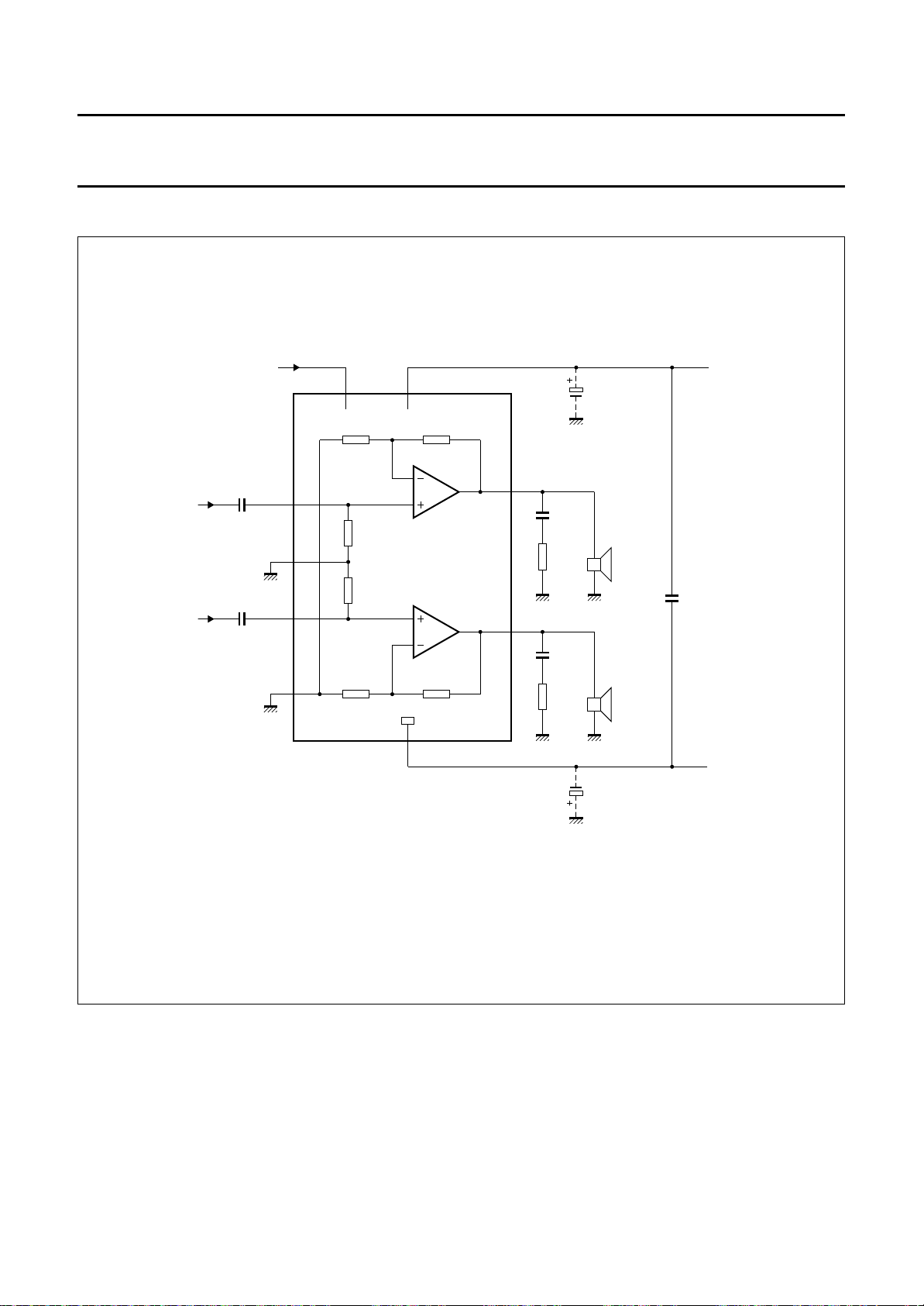
TEST AND APPLICATION INFORMATION
V
V
I
I
mute input
220 nF
220 nF
+ V
P
22 nF
8.2 Ω
22 nF
8.2 Ω
2200 µF
R = 8 Ω
R = 8 Ω
2200 µF
L
100 nF
L
– V
MLA710 - 2
P
72
20 kΩ680 Ω
1
20 kΩ
3
20 kΩ
9
8
TDA2615
20 kΩ680 Ω
5
4
6
1995 May 08 8
Fig.4 Test and application circuit with symmetrical power supply.
Page 9
Philips Semiconductors Product specification
2 × 6 W hi-fi audio power amplifier TDA2615
V
V
I
100 µF
I
mute input
220 nF
220 nF
V
P
100 nF
4
22 nF
8.2 Ω
6
22 nF
8.2 Ω
internal
1/2 V
72
P
5
20 kΩ680 Ω
TDA2615
20 kΩ680 Ω
2
1
20 kΩ
3
20 kΩ
9
8
R
S
2200 µF
680 µF
R = 8 Ω
L
680 µF
R = 8 Ω
L
MLA709 - 1
V
S
1995 May 08 9
Fig.5 Test and application circuit with asymmetrical power supply.
Page 10
Philips Semiconductors Product specification
2 × 6 W hi-fi audio power amplifier TDA2615
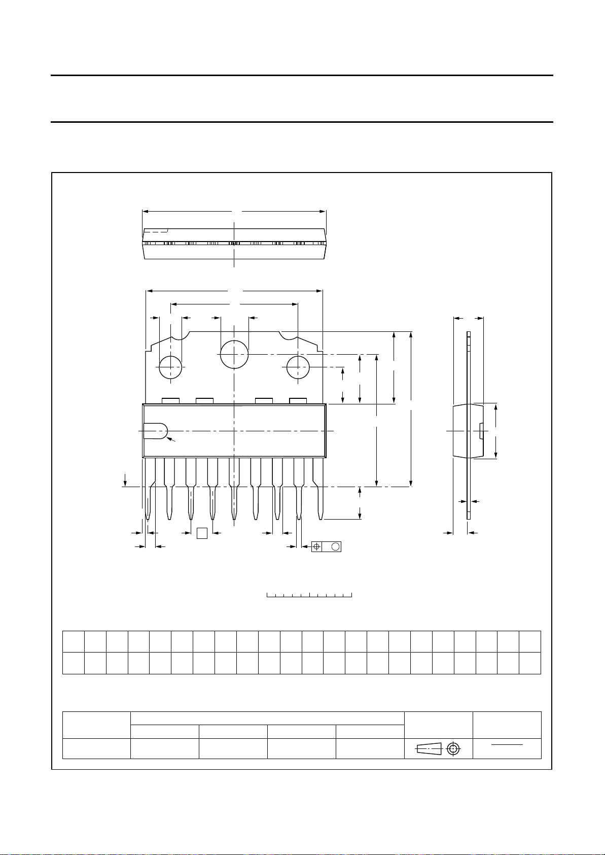
PACKAGE OUTLINE
SIL9MPF: plastic single in-line medium power package with fin; 9 leads
D
D
1
q
P
pin 1 index
P
1
q
2
q
1
SOT110-1
A
2
A
3
A
A
4
E
seating plane
19
Z
b
e
2
b
b
1
0 5 10 mm
scale
DIMENSIONS (mm are the original dimensions)
UNIT
mm
A
18.5
17.8
max.
3.7
2
A
8.7
8.0
A
3
4
15.8
15.4
b
0.67
0.50
b
1
2
1.40
1.14
bcD
1.40
1.14
0.48
0.38
(1)
21.8
21.4
D
21.4
20.7
1
A
Note
1. Plastic or metal protrusions of 0.25 mm maximum per side are not included.
OUTLINE
VERSION
IEC JEDEC EIAJ
REFERENCES
SOT110-1
w M
(1)
E
eLPP
6.48
6.20
2.54
3.9
3.4
L
c
Q
(1)
w
0.25
Z
max.
1.0
2.75
2.50
1
3.4
3.2
q
Q
1.75
15.1
1.55
14.9
EUROPEAN
PROJECTION
q1q
2
5.9
4.4
5.7
4.2
ISSUE DATE
92-11-17
95-02-25
1995 May 08 10
Page 11

Philips Semiconductors Product specification
2 × 6 W hi-fi audio power amplifier TDA2615
SOLDERING
Plastic single in-line packages
Y DIP OR WAVE
B
The maximum permissible temperature of the solder is
260 °C; this temperature must not be in contact with the
joint for more than 5 s. The total contact time of successive
solder waves must not exceed 5 s.
The device may be mounted up to the seating plane, but
the temperature of the plastic body must not exceed the
specified storage maximum. If the printed-circuit board has
DEFINITIONS
Data sheet status
Objective specification This data sheet contains target or goal specifications for product development.
Preliminary specification This data sheet contains preliminary data; supplementary data may be published later.
Product specification This data sheet contains final product specifications.
Limiting values
Limiting values given are in accordance with the Absolute Maximum Rating System (IEC 134). Stress above one or
more of the limiting values may cause permanent damage to the device. These are stress ratings only and operation
of the device at these or at any other conditions above those given in the Characteristics sections of the specification
is not implied. Exposure to limiting values for extended periods may affect device reliability.
been pre-heated, forced cooling may be necessary
immediately after soldering to keep the temperature within
the permissible limit.
EPAIRING SOLDERED JOINTS
R
Apply the soldering iron below the seating plane (or not
more than 2 mm above it). If its temperature is below
300 °C, it must not be in contact for more than 10 s; if
between 300 and 400 °C, for not more than 5 s.
Application information
Where application information is given, it is advisory and does not form part of the specification.
LIFE SUPPORT APPLICATIONS
These products are not designed for use in life support appliances, devices, or systems where malfunction of these
products can reasonably be expected to result in personal injury. Philips customers using or selling these products for
use in such applications do so at their own risk and agree to fully indemnify Philips for any damages resulting from such
improper use or sale.
1995 May 08 11
 Loading...