

Page 1
UNISONIC TECHNOLOGIES CO., LTD
TDA2003
10W CAR RADIO AUDIO AMPLIFIER
DESCRIPTION
The UTC TDA2003 is a monolithic audio power amplifier
integrated circuit.
FEATURES
*Very Low External Component Required.
*High Current Output ( up to 3 A).
*Low Harmonic and Crossover Distortion.
*Built-in Over Temperature Protection.
*Short Circuit Protection Between all Pins.
ORDERING INFORMATION
Ordering Number
Lead Free Halogen Free
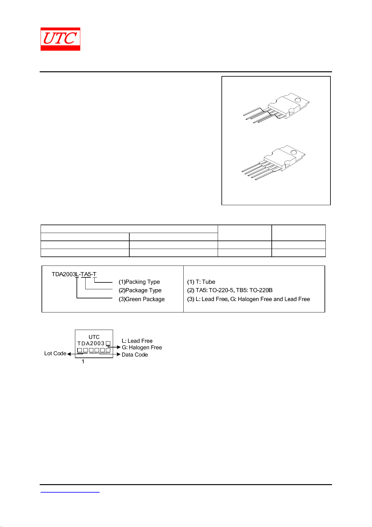
TDA2003L-TA5-T TDA2003G-TA5-T TO-220-5 Tube
TDA2003L-TB5-T TDA2003G-TB5-T TO-220B Tube
LINEAR INTEGRATED CIRCUIT
1
TO-220B
1
TO-220-5
Package Packing
MARKING
www.unisonic.com.tw 1 of 10
Copyright © 2015 Unisonic Technologies Co., Ltd QW-R107-002.H
Page 2
UNISONIC TECHNOLOGIES CO., LTD
TDA2003
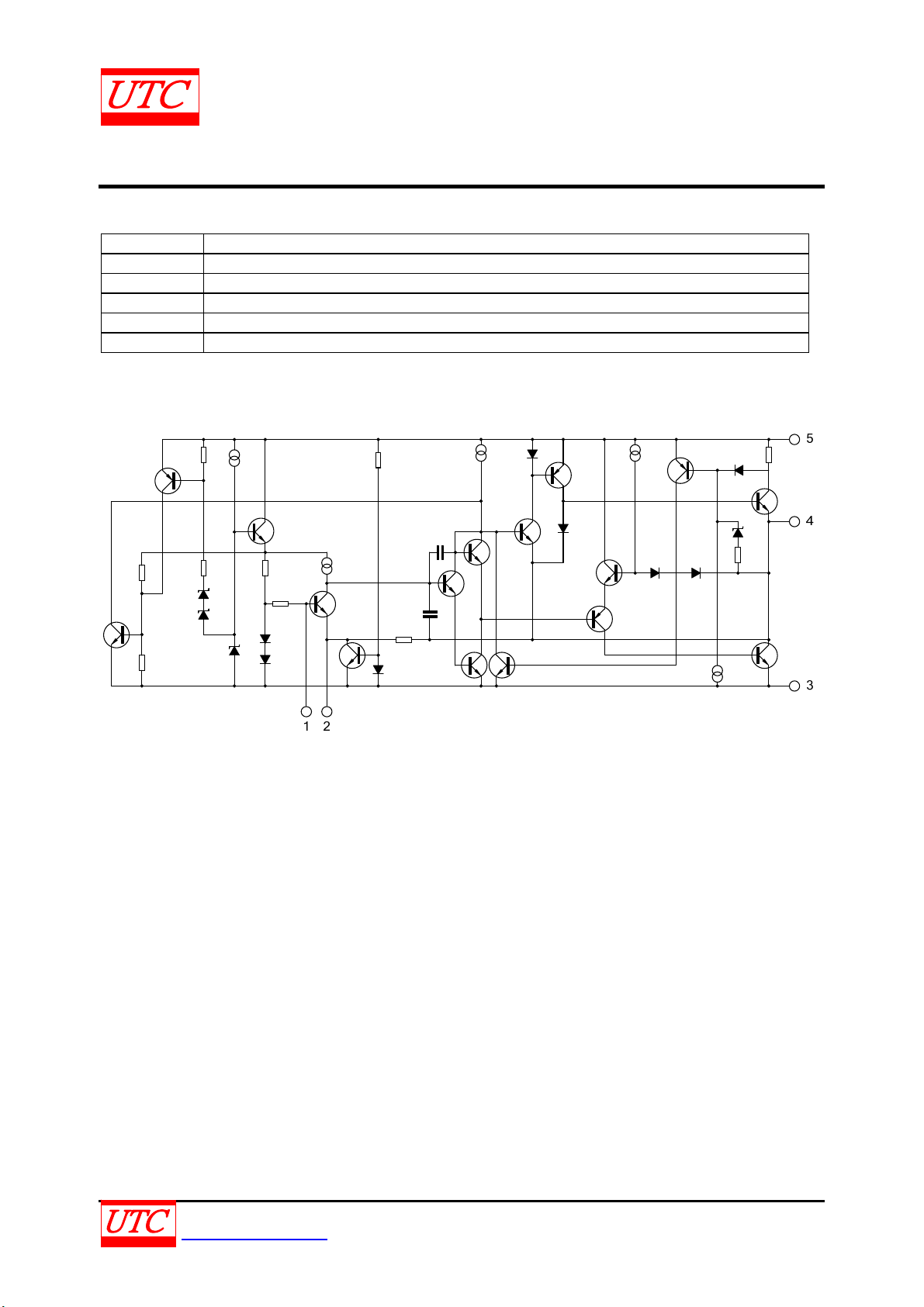
PIN DESCRIPTION
PIN NO. PIN NAME
1 Non inverting input
2 Inverting input
3 Ground
4 Output
5 Supply Voltage
BLOCK DIAGRAM
LINEAR INTEGRATED CIRCUIT
UNISONIC TECHNOLOGIES CO., LTD 2 of 10
www.unisonic.com.tw QW-R107-002.H
Page 3
TDA2003 LINEAR INTEGRATED CIRCUIT
)
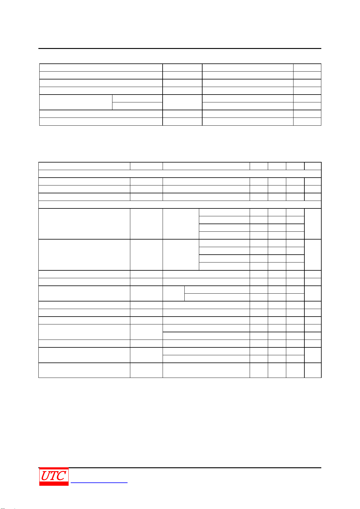
ABSOLUTE MAXIMUM RATINGS (T
=25C, unless otherwise specified)
A
PARAMETER SYMBOL RATINGS UNIT
Peak Supply Voltage VSS 40 V
DC Supply Voltage VSS 28 V
Operating Supply Voltage VSS 18 V
Output Peak Current
Repetitive
Non Repetitive 4.5 A
I
O(PEAK)
3.5 A
Power Dissipation at TC= 90C PD 20 W
Storage and Junction Temperature T
-40 ~ +150 C
STG
Note: Absolute maximum ratings are those values beyond which the device could be permanently damaged.
Absolute maximum ratings are stress ratings only and functional device operation is not implied.
ELECTRICAL CHARACTERISTICS
(TA=25C, Refer to the test circuit, VS=16V, unless otherwise specified.)
PARAMETER SYMBOL TEST CONDITIONS MIN TYP MAX UNIT
DC CHARACTERISTICS
Supply Voltage VSS 8 18 V
Quiescent Output Voltage V
Quiescent Drain Current ID 44 50 mA
AC CHARACTERISTI CS
Output Power P
Input Sensitivity VI f=1kHz
Input Saturation Voltage V
Frequency Response(-3dB) F P
Total Harmonic Distortion THD f=1kHz
Input Resistance(Pin 1) RI Open Loop, f=1kHz 70 150 kΩ
Input Noise Current iN 60 200 pA
Input Noise Voltage eN 1 5 μV
Open Loop Voltage Gain Gvo
Closed Loop Voltage Gain Gvc f=1kHz, RL=4Ω 39.3 40 40.3 dB
Efficiency, f=1kHz η
Supply Voltage Rejection SVR
6.1 6.9 7.7 V
OUT
R
=4Ω 5.5 6
L
OUT
THD=10%,
f=1kHz
RL=2Ω 9 10
RL=3.2Ω 7.5
RL=1.6Ω 12
P
=0.5W, RL=4Ω 14
OUT
P
=6W, RL=4Ω 55
OUT
P
=0.5W, RL=2Ω 10
OUT
P
=10W, RL=2Ω 50
OUT
300 mV
I(RMS
=1W, RL=4Ω 40 15000 Hz
OUT
P
=0.05 ~ 4.5W, RL=4Ω 0.15
OUT
P
=0.05 ~ 7.5W, RL=2Ω 0.15
OUT
f=1kHz 80 dB
f=10kHz 60 dB
P
=6W, RL=4Ω 69
OUT
P
=10W, RL=2Ω 65
OUT
f=100Hz, V
R
=10kΩ, RL=4Ω
G
RUPPLE
=0.5V
30 36 dB
W
mV
%
%
UNISONIC TECHNOLOGIES CO., LTD 3 of 10
www.unisonic.com.tw QW-R107-002.G
Page 4
TDA2003 LINEAR INTEGRATED CIRCUIT
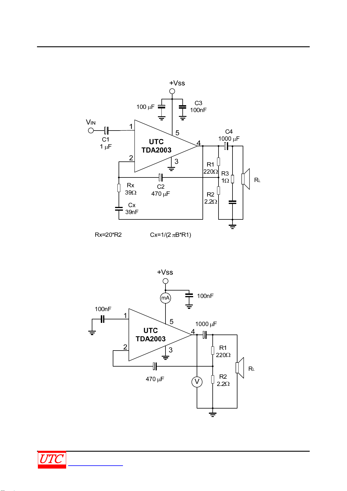
TEST CIRCUIT
AC Test Circuit
DC Test Circuit
100nF
UNISONIC TECHNOLOGIES CO., LTD 4 of 10
www.unisonic.com.tw QW-R107-002.G
Page 5
TDA2003 LINEAR INTEGRATED CIRCUIT
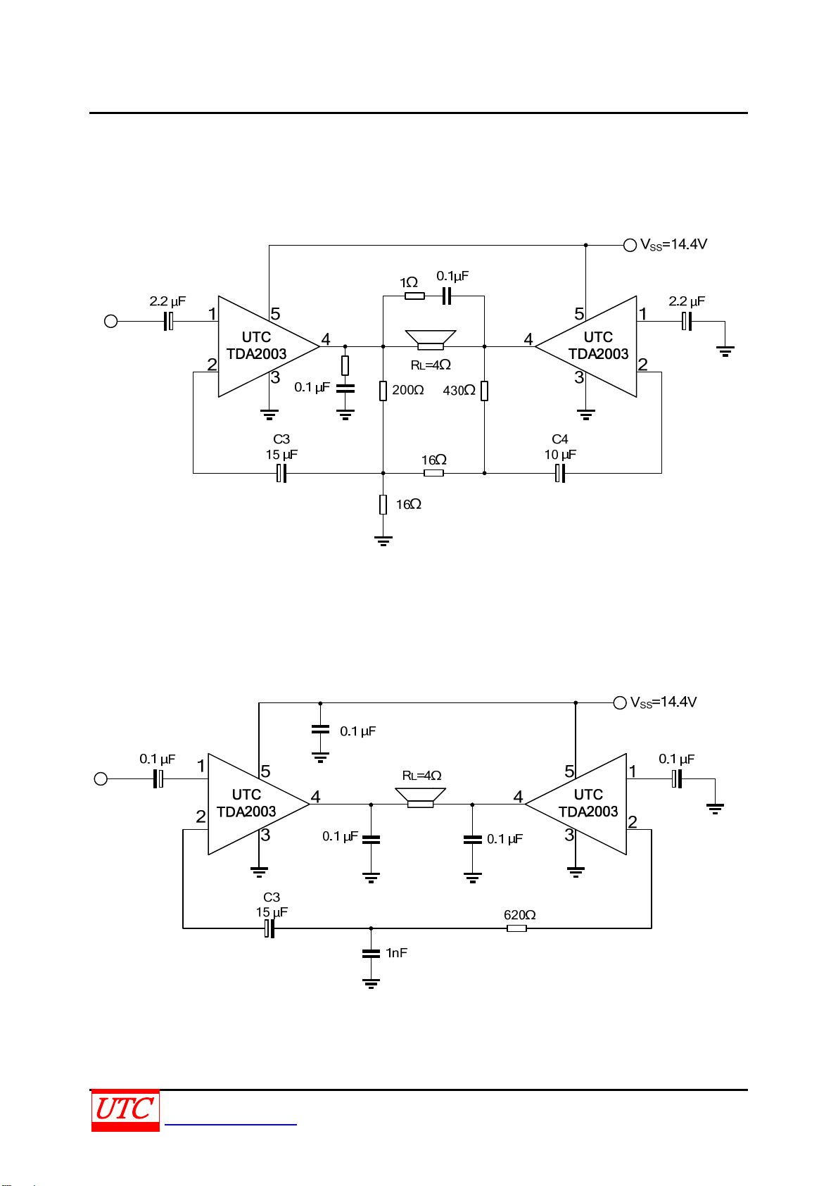
TYPICAL APPLICATION CIRCUIT
20W Bridge Configuration Application
The Values of the capacitors C3 and C4 are different to optimize the SVR (Typ. 40dB)
TYPICAL APPLICATION CIRCUIT
Low Cost Bridge Configuration Application Circuit(P
OUT
=18W)
UNISONIC TECHNOLOGIES CO., LTD 5 of 10
www.unisonic.com.tw QW-R107-002.G
Page 6
TDA2003 LINEAR INTEGRATED CIRCUIT
BUILT-IN PROTECTION SYSTEMS
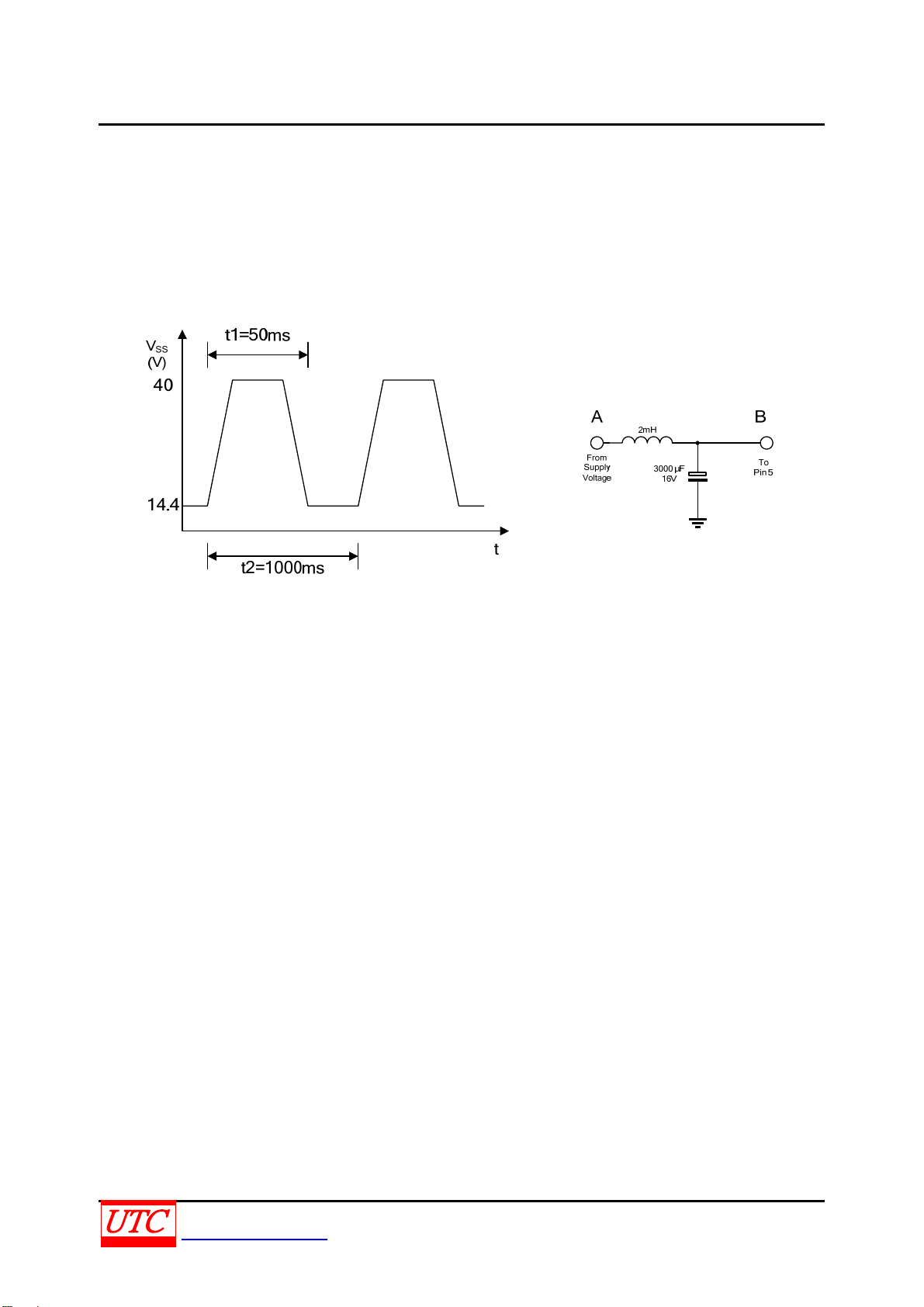
LOAD DUMP VOLTAGE SURGE
The UTC TDA2003 has a circuit which enables it to withstand a voltage pulse train, on pin 5.
If the supply voltage peaks to more than 40V, then an LC filter must be inserted between the supply and pin 5, in
order to assure that the pulses at pin 5 will be head within the limits.
A suggested LC network. With this network, a train of pulses with amplitude up to 120V and width of 2ms can be
applied at point A. This type of protection is ON when the supply voltage(pulsed or DC) exceeds 18V. For this
reason the maximum operating supply voltage is 18V.
SHORT CIRCUIT (AC and DC Conditions)
The UTC TDA2003 can withstand a permanent short-circuit on the output for a supply voltage up to 16V.
POLARITY INVERSION
High current (up to 5A) can be handled by the device with no damage for a longer period than the blow-out time
of a quick 1A fuse(normally connected in series with the supply).
The feature is added to avoid destruction if, during fitting to the car, a mistake on connection of the supply is made.
OPEN GROUND
When the radio is in the ON condition and the ground is accidentally opened, a standard audio amplifier will be
damaged. On the UTC TDA2003 protection diodes are included to avoid any damage.
INDUCTIVE LOAD
A protection diode is provide between pin 4 and pin 5(see the internal schematic diagram) to allow use of the
UTC TDA2003 with inductive loads. In particular, the UTC TDA2003 can drive a coupling transformer for audio
modulation.
DC VOLTAGE
The maximum operating DC voltage on the UTC TDA2003 is 18V.
However the device can withstand a DC voltage up to 28V with no damage. This could occur during winter if two
batteries were series connected to crank the engine.
THERMAL SHUT-DOWN
The presence of a thermal limiting circuit offers the following advantages:
(1) An overload on the output (even if it is permanent),or an excessive ambient temperature can be easily withstood.
(2) The heat-sink can have a smaller factor compared with that of a conventional circuit. There is no device damage
in case of excessive junction temperature: all that happens is that Po ( and therefore P
) and Id are reduced.
D
UNISONIC TECHNOLOGIES CO., LTD 6 of 10
www.unisonic.com.tw QW-R107-002.G
Page 7

TDA2003 LINEAR INTEGRATED CIRCUIT
COMPONENTS USAGE SUGGESTION
The recommended values of the components are those shown on typical application circuit Different values can
be used. The following table can help the designer.
COMPONENT
R1 (Gv-1)×R2 gain setting. increase of drain current
R2 2.2Ω gain and SVR setting. Decrease of SVR
R3 1Ω Frequency stability
Rx 20R2 Upper frequency cutoff
C1 2.2μF Input DC decoupling
C2 470μF Ripple rejection Decrease of SVR
C3 0.1μF Supply voltage bypass Danger of oscillation
C4 1000μF Supply voltage bypass
C5 0.1μF Frequency stability
Cx 1/(2×B×R1) Upper frequency cutoff Lower bandwidth Larger bandwidth
RECOMMENDED
VALUE
PURPOSE
LARGE THAN
RECOMMENDED VALUE
Danger of oscillation at high
frequencies with inductive
loads.
Poor high frequencies
attenuation
SMALLER THAN
RECOMMENDED VALUE
Danger of oscillation
Noise at switch-on
switch-off
Higher low frequency
cutoff
Danger of oscillation at
high frequencies with
inductive loads.
UNISONIC TECHNOLOGIES CO., LTD 7 of 10
www.unisonic.com.tw QW-R107-002.G
Page 8
TDA2003 LINEAR INTEGRATED CIRCUIT
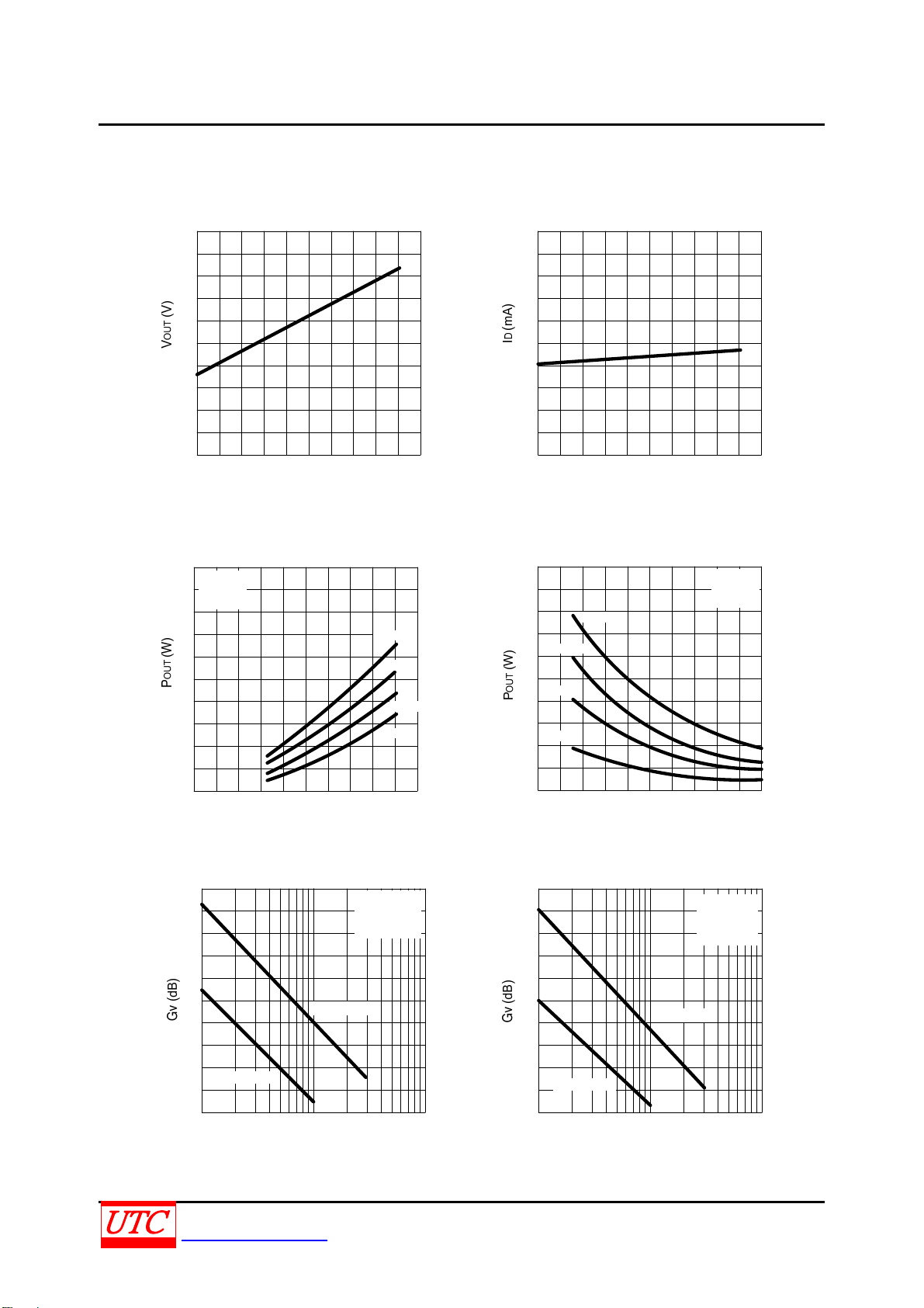
TYPICAL CHARACTORISTICS
Quiescent output voltage vs.Supply
voltage
Quiescent drain current vs.Supply
voltage
8
6
4
2
0
810 12 14 16
VS (V)
Output power vs.Supply voltage
Gv=40dB
f=1kHz
THD=10%
20
15
10
R=1.6Ω
R=2Ω
R=3.2Ω
80
60
40
20
0
810 12 14 16
VS(V)
Output power vs.load resistance
Gv=40dB
f=1kHz
16
12
8
VS=16V
VS=14.4V
VS=12V
THD=10%
5
0
05 1015 20
VS(V)
Gain vs. Input sensitivity
58
54
52
48
44
40
36
32
28
P
=0.5W
OUT
24
20
10 100 1000
VI (RMS) (mV) VI (RMS) (mV)
P
OUT
VS=14.4V
f=1kHz
R
=6W
=4Ω
L
R=4Ω
VS=8V
4
0
02 4 6 8
RL (Ω)
Gain vs. Input sensitivity
58
P
OUT
VS=14.4V
f=1kHz
R
=10W
L
54
52
48
44
40
36
32
28
P
=0.5W
OUT
24
20
10
100 1000
=2Ω
UNISONIC TECHNOLOGIES CO., LTD 8 of 10
www.unisonic.com.tw QW-R107-002.G
Page 9
TDA2003 LINEAR INTEGRATED CIRCUIT
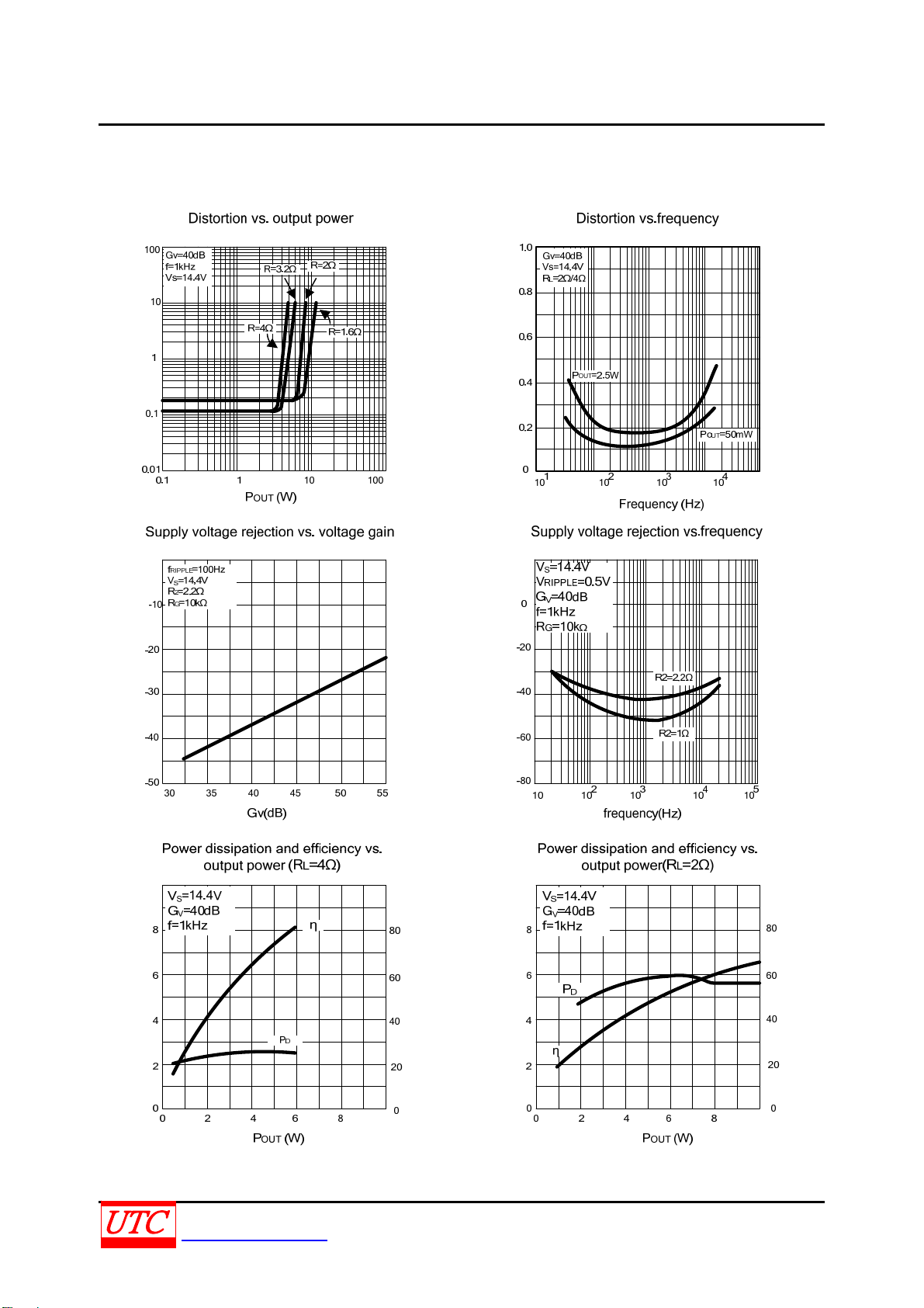
TYPICAL CHARACTORISTICS (Cont.)
THD (%)
SVR (dB)
THD (%)
SVR (dB)
η (%)
PD (W)
PD (W)
η (%)
UNISONIC TECHNOLOGIES CO., LTD 9 of 10
www.unisonic.com.tw QW-R107-002.G
Page 10
TDA2003 LINEAR INTEGRATED CIRCUIT
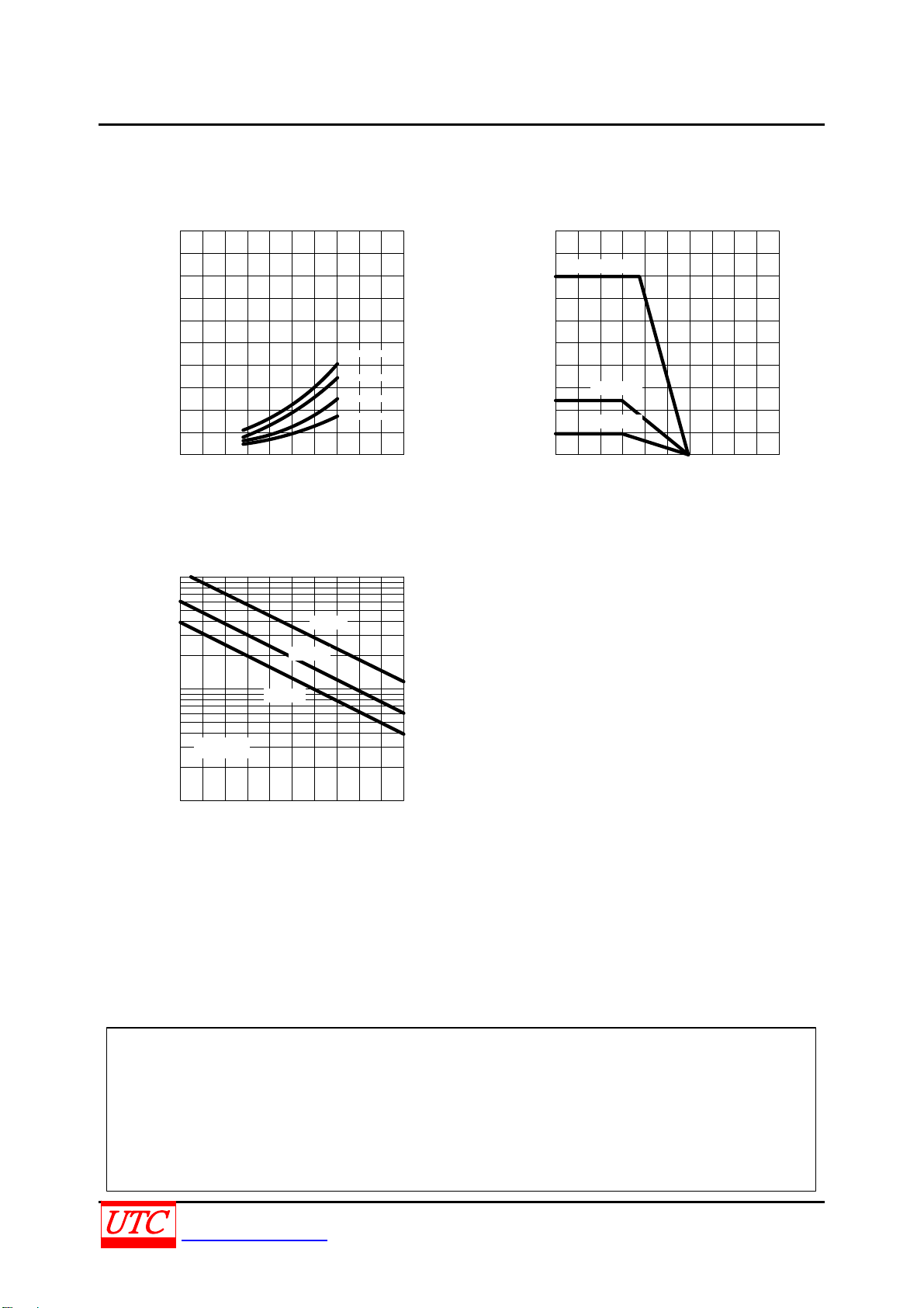
TYPICAL CHARACTORISTICS (Cont.)
Maximum Power dissipation and
supply voltage(sine wave operation)
Maximum allowable dissipation
and ambient temperature
20
15
PD (W)
10
5
0
0 5 10 15 20
Vs(V)
RL=1.6Ω
RL=2Ω
RL=3.2Ω
RL=4Ω
Typical values of capacitor(Cx) for
different values of frequency response
100
B=10kHz
B=15kHz
10
Cx (nF)
B=20kHz
infinite heatsink
20
15
D (W)
P
10
10°C/W
5
30°C/W
0
0 50 100 150 200
TA(°C)
R2=2.2Ω
1
36 40 44 48
Gv (dB)
UTC assumes no responsibility for equipment failures that result from using products at values that
exceed, even momentarily, rated values (such as maximum ratings, operating condition ranges, or
other parameters) listed in products specifications of any and all UTC products described or contained
herein. UTC products are not designed for use in life support appliances, devices or systems where
malfunction of these products can be reasonably expected to result in personal injury. Reproduction in
whole or in part is prohibited without the prior written consent of the copyright owner. The information
presented in this document does not form part of any quotation or contract, is believed to be accurate
and reliable and may be changed without notice.
UNISONIC TECHNOLOGIES CO., LTD 10 of 10
www.unisonic.com.tw QW-R107-002.G
 Loading...