

Page 1

INTEGRATED CIRCUITS
DATA SH EET
TDA1602A
Double-deck playback/record IC
(DDPR)
Product specification
File under Integrated Circuits, IC01
April 1992
Page 2

Philips Semiconductors Product specification
Double-deck playback/record IC (DDPR) TDA1602A
FEATURES
• Two stereo playback preamplifiers
• Stereo playback amplifier
• High speed dubbing headswitch for channel A
• Record/playback headswitch for channel B
• Dubbing switch
• Stereo record amplifier
• Automatic level control
• Erase and bias oscillator
• Tape selector
• Reference voltage source (1/2 VP)
• Logic part.
ORDERING INFORMATION
EXTENDED TYPE
NUMBER
TDA1602A 40 DIL plastic SOT129
Note
1. SOT129-1; 1996 August 29.
PINS PIN POSITION MATERIAL CODE
GENERAL DESCRIPTION
The TDA1602A is a Dolby B compatible recorder IC, which
has been designed for use in double-deck recorders for
Ferro/Chrome with high speed dubbing. The device
performs all the basic recorder functions and needs only a
very simple peripheral circuit of a few components. The
DDPR may also be used in applications with automatic
reverse.
All functions of the DDPR are selected by externally
applied DC voltage levels. The circuit is designed for use
with a mains-fed asymmetrical power supply but can also
be used with a symmetrical power supply (because of its
own 1/2 VP reference voltage source).
PACKAGE
(1)
April 1992 2
Page 3
Philips Semiconductors Product specification
Double-deck playback/record IC (DDPR) TDA1602A
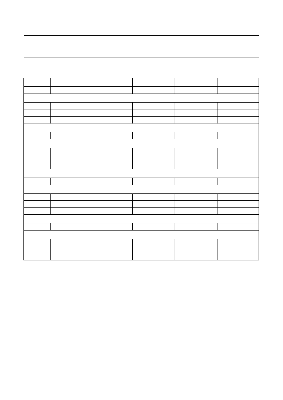
QUICK REFERENCE DATA
All voltages referenced to pin 12, all currents positive into the IC
SYMBOL PARAMETER CONDITIONS MIN. TYP. MAX. UNIT
V
P
Playback amplifier
G gain f = 315 Hz − 57 − dB
S/N signal-to-noise ratio − 53 − dB
THD total harmonic distortion V
Headswitch
V
ON(p-p)
Record amplifier
G gain f = 315 Hz − 14 − dB
S/N signal-to-noise ratio − 65 − dB
THD total harmonic distortion V
Automatic level control
∆V
O
Oscillator
f
OSC
I
O(peak)
V
O(p-p)
Reference voltage
V
ref
Logic part
I
I
supply voltage range 7.0 − 18.0 V
= 150 mV − 0.1 − %
O
maximum voltage (peak-to-peak value) record mode −−90 V
= 1.5 mV − 0.3 − %
Orecord
output voltage variation ∆V
= 20 dB − 1 − dB
line
frequency range 60 − 120 kHz
output current (peak value) 140 −−mA
output voltage (peak-to-peak value) −−36 V
output voltage − 1/2 V
P
− V
input current
pins 8 and 10 − 100 −µA
pins 7 and 9 −−900 µA
April 1992 3
Page 4
Philips Semiconductors Product specification
Double-deck playback/record IC (DDPR) TDA1602A
handbook, full pagewidth
connection for high speed
dubbing capacitor left
signal ground for deck A
connection for high speed
dubbing capacitor right
deck A right input
playback equalization
left: HF adjustment
playback equalization
right: HF adjustment
record equalization
right: HF adjustment
record equalization
right: LF adjustment
record amplifier right output
deck A left
input
playback equalization
left: LF adjustment
38
LS/HS
37
36
35
LS/HS
34
33
32
31
21
29
AL
A
AR
LS/HS
AHS
BR
∑
BL
L
Fe/Cr
∑
R
Fe/Cr LS/HS
ALC
R
L
playback equalization
right: LF adjustment
39 40
LS/HS
TDA1602A
VR
VR
1/2
1/2
S/M
1
line out left
2
line out right
3
line in right
4
source-selector out
right
5
source-selector out left
record amplifier left output
record equalization
left: HF adjustment
record equalization
left: LF adjustment
deck B left input:
connection input playback
deck B left input:
connection HF biasing
signal ground for deck B
deck B right input:
connection HF biasing
deck B right input:
connection input playback
VTR
28
30
22
27
P/R
26
25
24
P/R
23
K
ALC
LS/HS
BL
B
BR
adjustment of limiting
and setting time
20 19
adjustment of
release time
S/M
Fe/Cr
LS/HS
R/P
LOGIC
S/M
A/B
Fe/Cr
P/R/HSR
I
V
V
control
OSCILLATOR
ref
ref
V–
V–
10
11
12
13
14
15
16
17
18
MLA335
6
line in left
signal/mute input
7
for line out
8
channel selection input
9
tape selection input
playback/record/high speed
record selection input
equalization adjustment
reference voltage source
ground; substrate
supply voltage
amplitude control
input for oscillator
oscillator output
oscillator ground
oscillator output
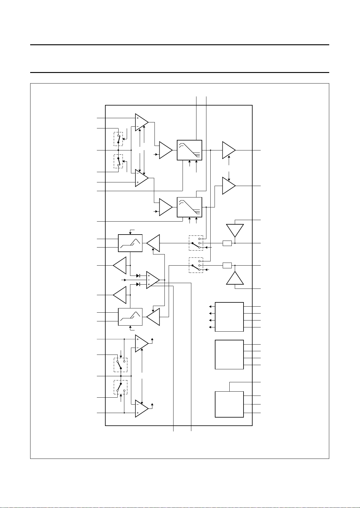
Fig.1 Block diagram.
April 1992 4
Page 5

Philips Semiconductors Product specification
Double-deck playback/record IC (DDPR) TDA1602A
PINNING
SYMBOL PIN DESCRIPTION
LOL 1 line out left
LOR 2 line out right
LIR 3 line in right
SOR 4 source-selector out right
SOL 5 source-selector out left
LIL 6 line in left
S/M 7 signal/mute input for line out
A/B 8 channel selection input
TS 9 tape selection input
P/R/HSR 10 playback/record/high-speed record selection input
EQUADJ 11 equalization adjustment
V
ref
GND 13 ground; substrate
V
P
OSCCON 15 amplitude control input for oscillator
OSCO1 16 oscillator output 1
OSCGND 17 oscillator ground
OSCO2 18 oscillator output 2
ADJRT 19 adjustment of release time
ADJLST 20 adjustment of limiting and setting time
RECERLF 21 record equalization right: LF adjustment
RECELLF 22 record equalization left: LF adjustment
BRIP 23 deck B right input: connection input playback
BRIBHF 24 deck B right input: connection HF biasing
SGNDB 25 signal ground for deck B
BLIBHF 26 deck B left input: connection HF biasing
BLIP 27 deck B left input: connection input playback
RECOL 28 record amplifier left output
RECOR 29 record amplifier right output
RECELHF 30 record equalization left: HF adjustment
RECERHF 31 record equalization right: HF adjustment
PERHF 32 playback equalization right: HF adjustment
PELHF 33 playback equalization left: HF adjustment
ARI 34 deck A right input
HSDR 35 connection for high speed dubbing capacitor right
SGNDA 36 signal ground for deck A
HSDL 37 connection for high speed dubbing capacitor left
ALI 38 deck A left input
PELLF 39 playback equalization left: LF adjustment
PERLF 40 playback equalization right: LF adjustment
12 reference voltage source
14 supply voltage
April 1992 5
Page 6

Philips Semiconductors Product specification
Double-deck playback/record IC (DDPR) TDA1602A
handbook, halfpage
P / R / HSR
EQUADJ
OSCCON
OSCGND
LOL
LOR
LIR
SOR
SOL
LIL
S / M
A / B
TS
V
GND
V
OSCO1
ref
1
2
3
4
5
6
7
8
9
10
TDA1602A
11
12
13
P
15
16
17
40
39
38
37
36
35
34
33
32
31
30
29
28
2714
26
25
24
PERLF
PELLF
ALI
HSDL
SGNDA
HSDR
ARI
PELHF
PERHF
RECERHF
RECELHF
RECOR
RECOL
BLIP
BLIBHF
SGNDB
BRIBHF
MLA336
23
22
21
BRIP
RECELLF
ADJRT
18
19
20
OSCO2
ADJLST RECERLF
Fig.2 Pin configuration.
April 1992 6
Page 7

Philips Semiconductors Product specification
Double-deck playback/record IC (DDPR) TDA1602A
FUNCTIONAL DESCRIPTION
Playback pre-amplifier
The playback preamplifier is a linear low-noise amplifier
with an internal fixed gain of 26.4 dB. The relevant
preamplifier for playback of channel A or B can be selected
externally.
Playback amplifier
The frequency response of the playback amplifier is
determined by two external capacitors (Right: C6 and C21,
Left: C5 and C20). The different equalization curves for
Ferro and Chrome (with time constants of 120 µs and 70
µs respectively) are controlled by the logic part of the
circuit.
High speed dubbing headswitch
This electronic switch is used to connect, or disconnect, an
extra external capacitor (Right: C4, Left: C1) in parallel
with the gap-loss correction capacitor.
Record/playback headswitch
This is a two position electronic switch which switches the
relevant side of the head to the signal ground.
ECORD POSITION
R
In the record mode the input of the playback amplifier is
switched to the signal ground. In this way the bias and
audio signal current can be applied to the head.
LAYBACK POSITION
P
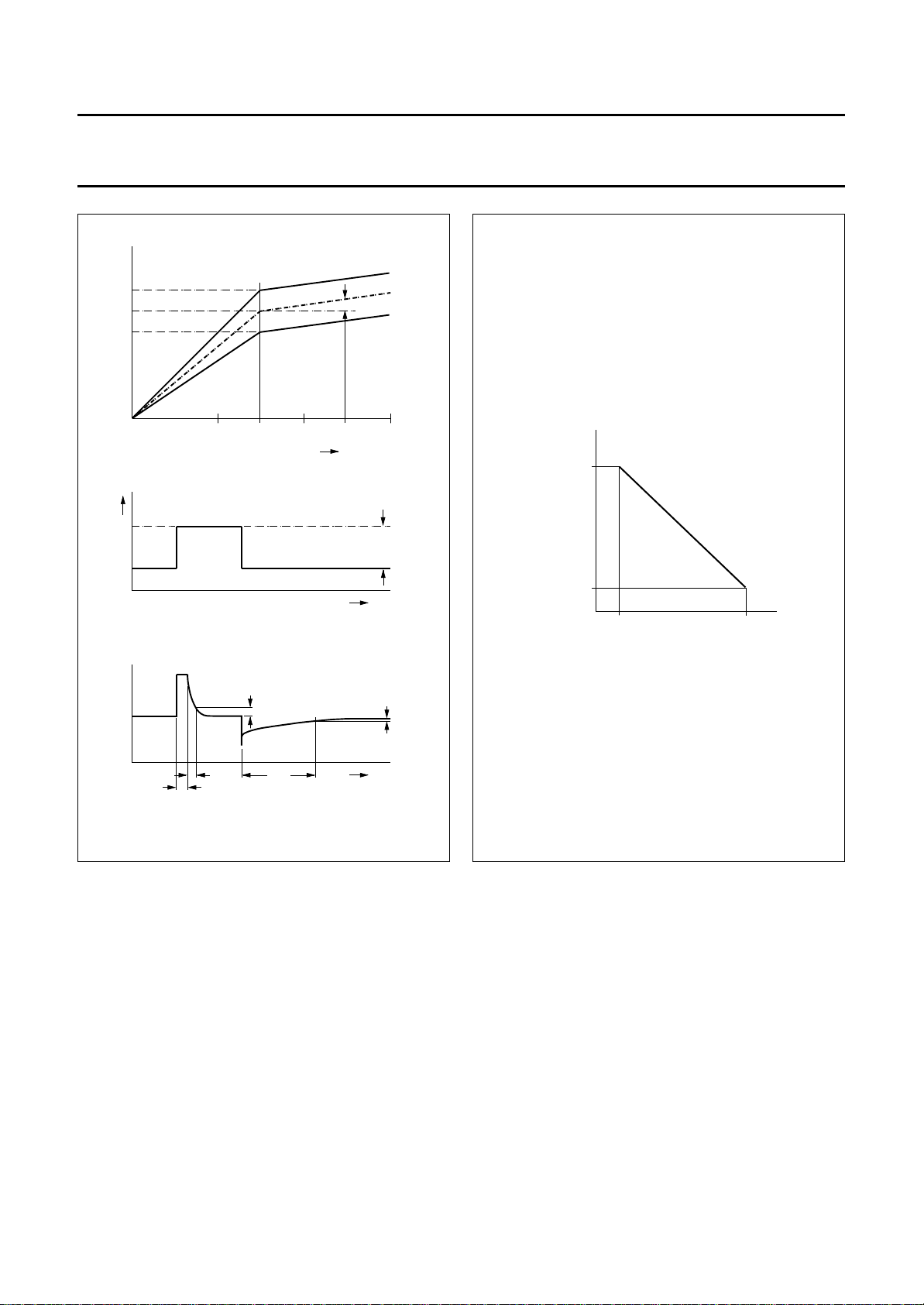
Automatic level control
The automatic level control (ALC) has a control range of 20
dB. The variation in the output voltage is less than 2 dB
(see Fig.5). The attack and recovery time of the ALC can
be adjusted externally.
Erase and bias oscillator
The erase and bias oscillator provides the following:
A high frequency bias current to enable a linear magnetic
recording process on the tape.
A sinusoidal voltage, the amplitude of which is determined
by the applied voltage at pin 15 (see also Fig.6).
The necessary current for erasing the tape which is only
activated when the circuit is switched to the record mode.
Reference voltage source
This circuit delivers an output voltage which is half the
supply voltage. The output voltage can be taken as signal
ground. In this way a symmetrical power supply is
available for the total recorder application.
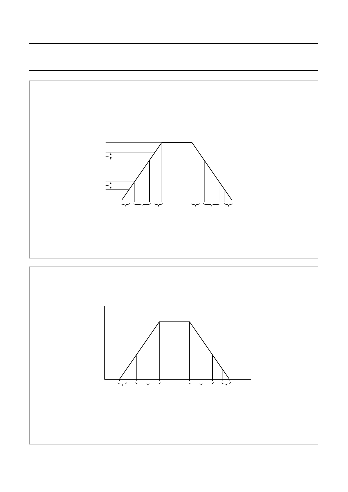
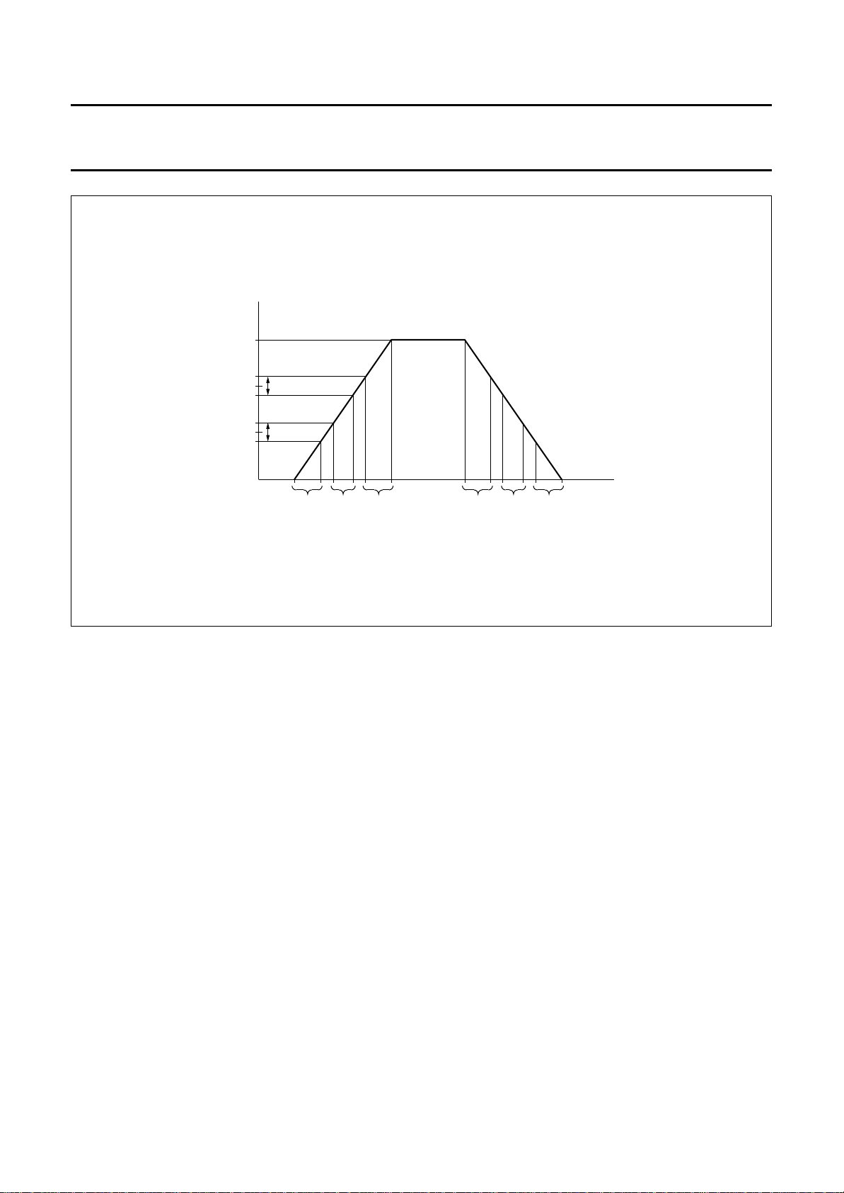
Logic part
The logic part converts the incoming information from the
logic input into the necessary switching signals, used in the
analog parts of the circuit. The conversion is determined
by the level of the input signal (see Fig.7). The logic inputs
(pins 8 and 10) are independent of signal rise and fall
times. The inputs at pins 7 and 9 enable smooth switching
between signal/mute and Ferro/Chrome respectively.
In the playback mode the biasing side of the head is
switched to the signal ground.
Record amplifier
The frequency response of the record amplifier is
determined by means of two external capacitors (Right:
C11 and C12; Left: C17 and C18).
By omitting these capacitors a flat frequency response is
obtained for Dolby application.
April 1992 7
Page 8

Philips Semiconductors Product specification
Double-deck playback/record IC (DDPR) TDA1602A
LIMITING VALUES
In accordance with the Absolute Maximum System (IEC 134). All voltages referenced to pin 12; all currents positive into
the IC
SYMBOL PARAMETER CONDITIONS MIN. MAX. UNIT
V
V
V
V
V
T
T
P
P
7-10
15
16,18
28,30
stg
j
tot
positive supply voltage − 18 V
logic input voltage (pins 7 to 10) 0 V
control input voltage (pin 15) 0 V
P
P
V
V
oscillator output voltage (pins 16 and 18) 0 36 V
headswitch voltage (pins 28 and 30) −45 +45 V
storage temperature range −55 +150 °C
junction temperature − +150 °C
total power dissipation T
= +60 °C − 1.8 W
amb
April 1992 8
Page 9

Philips Semiconductors Product specification
Double-deck playback/record IC (DDPR) TDA1602A
DC CHARACTERISTICS
All voltages referenced to pin 12; all currents positive into the IC; All parameters are measured in the test circuit (Fig.1 1)
at nominal supply voltage (V
= 25 °C; unless otherwise specified
T
amb
SYMBOL PARAMETER CONDITIONS MIN. TYP. MAX. UNIT
Supplies
V
P
I
P
supply voltage range 7.0 − 18.0 V
supply current note 1
Playback amplifier (Fe02/Cr02)
G gain at normal speed f = 315 Hz 55 57 59 dB
B frequency response with respect to gain f = 30 Hz 10 12 14 dB
left/right balance −1 0 +1 dB
A/B balance −1 0 +1 dB
G gain at double speed f = 630 Hz 49 51 53 dB
B frequency response with respect to gain f = 60 Hz 10 12 14 dB
left/right balance −1 0 +1 dB
V
O
nominal output voltage note 2; VI= 200 µV − 150 − mV
THD total harmonic distortion V
S/N signal-to-noise ratio note 3; weighted curve;
left/right separation V
SVRR supply voltage ripple rejection V
input impedance 100 −−kΩ
Z
I
I
bias
V
O
input bias current − 0.5 −µA
DC output voltage with respect to V
(V
and V
1-12
A/B separation note 4 − 340 −µV
suppression of output signal V
(channel A and B)
= 15 V); f = 315 Hz; tape selectors at Fe02 position; normal speed; non-Dolby application;
P
playback mode 35 39 43 mA
record mode 39 43 47 mA
Cr02, f = 10 kHz −18 −17 −16 dB
Fe02, f = 10 kHz −13.5 −12.5 −11.5 dB
Cr02; f = 20 kHz −18 −17 −16 dB
Fe02; f = 20 kHz −13.5 −12.5 −11.5 dB
= 200 µV − 0.1 0.3 %
I
= 280 µV −−1%
V
I
51 53 − dB
20 Hz to 20 kHz
weighted curve
− 60 − dB
A(IEC179)
= 150 mV 40 50 − dB
O
= 100 mV; − 25 − dB
ripple
f = 100 Hz
−30 0 +30 mV
2-12
ref
)
note 5 − tbf − mV
7
= V
P
− 90 − dB
April 1992 9
Page 10

Philips Semiconductors Product specification
Double-deck playback/record IC (DDPR) TDA1602A
SYMBOL PARAMETER CONDITIONS MIN. TYP. MAX. UNIT
Record/playback headswitch
impedance ON
Z
ON
playback mode between pins 26 and 25
and pins 24 and 25;
I = 100 µA(RMS)
record mode between pins 27 and 25
and pins 23 and 25;
I = 1.5 mA(RMS)
I
IL
OFF-state leakage current voltage on pins 24 and
26 of VDC= ±45 V with
respect to V
high-speed dubbing headswitch normal speed, between
Z
ON
pins 35 and 36 and pins
36 and 37;
I = 100 µA(RMS)
(pin 12)
ref
− 35 100 Ω
− 25 50 Ω
− 1.0 2.5 µA
− 100 1000 Ω
Record amplifier (ALC off)
G gain at normal speed f = 315 Hz
note 6 13 14 15 dB
note 7 − 20 − dB
B frequency response with respect to gain f = 10 kHz 8.5 10.0 11.5 dB
Dolby; f = 10 kHz
note 6 13 14 15 dB
note 7 − 20 − dB
left/right balance −1 0 +1 dB
G gain at double speed note 7; f = 630 Hz 19 20 21 dB
B frequency response with respect to gain f = 20 kHz 8 10 12 dB
left/right balance −1 0 +1 dB
V
O
maximum output voltage V
= 800 mV;
Osel
− 4.0 − V
f = 1 kHz; THD = 3%
THD total harmonic distortion ALC switch ON;
f = 1 kHz
= 1 V −−0.7 %
V
Osel
= 3 V − 0.5 − %
V
Osel
S/N signal-to-noise ratio note 8; weighted curve − 60 − dB
20 Hz to 20 kHz
weighted curve − 65 − dB
A(IEC179)
Dolby; weighted curve 70 73 − dB
20 Hz to 20 kHz
left/right separation V
SVRR supply voltage ripple rejection V
= 300 mV 40 50 − dB
Osel
ripple
= 100 mV;
− 30 − dB
f = 100 Hz
April 1992 10
Page 11
Philips Semiconductors Product specification
Double-deck playback/record IC (DDPR) TDA1602A
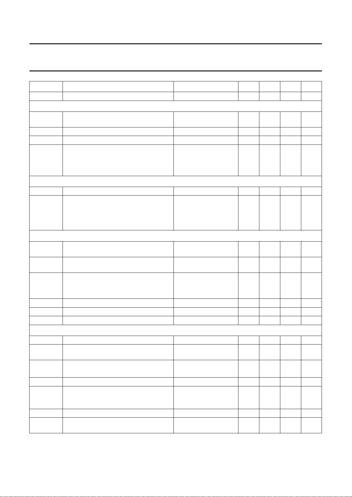
SYMBOL PARAMETER CONDITIONS MIN. TYP. MAX. UNIT
ZI input impedance 100 −−kΩ
Record amplifier (ALC off)
V
O
R
L
output impedance note 9 − tbf −Ω
Z
O
DC output voltage with respect to V
ref
load impedance on the output 10 −−kΩ
suppression of line input dubbing mode;
Source-selector
I
bias
input bias current − 15 − nA
S/N signal-to-noise ratio note 10; weighted curve 77 90 − dB
normal speed record,
V
and V
28-12
29-12
−30 0 30 mV
− tbf − dB
= 300 mV
V
Osel
deck B in playback;
V
= 300 mV
Osel
− tbf − dB
20 Hz to 20 kHz
weighted curve − 96 − dB
A(IEC179)
Automatic Level Control (ALC); see Fig.5
V
Iref
input reference voltage for ALC start
operation
V
Oref
output reference voltage ALC switched ON;
∆V output voltage variation V
t
l
t
s
t
r
limiting time ∆V
setting time − 2 − ms
release time − 10 − s
Erase and bias oscillator
f
OSC
I
O(p-p)
oscillator frequency note 11 − 80 − kHz
maximum output current pins 16 and 18
(peak-to-peak value)
V
OSC
output voltage pins 16 to 17 and pins 17 to VP= 18 V −−36 V
18 (peak-to-peak value)
V
V
I
15
OSC
I
voltage control range note 12 2.0 − 13.0 V
peak output voltage see Fig.6;
input current of control inputs − 0.1 −µA
THD total harmonic distortion between pins 16
and 18
− 300 − mV
1.35 1.5 1.65 V
V
= 300 mV
OseI
= 330 mV
OseI
= 10 dB − 0.2 1 dB
∆V
OseI
= 20 dB − 1 − dB
∆V
OseI
= 10 dB − 1 − ms
OseI
140 −−mA
− 8.0 − V
V
= VP−8 V
control
between pins 16 and 18
= 80 mA − 0.5 − %
I
O
April 1992 11
Page 12

Philips Semiconductors Product specification
Double-deck playback/record IC (DDPR) TDA1602A
SYMBOL PARAMETER CONDITIONS MIN. TYP. MAX. UNIT
Reference voltage source
V
12
∆V
12
Logics inputs (pins 7 to 10); see Figs 7, 8 and 9
I
7
V
7
I
8
I
9
V
9
I
10
V
10
output voltage note 13;
no external load
output voltage deviation ∆I
= 1 mA −100 −+100 mV
ref
signal/mute input current V7= V
signal/mute input voltage
signal 0 − 0.3 V
mute 6.0 − 15.0 V
input current for channel A/B selection V8= V
input voltage for channel A/B selection
deck A 0 − 3.0 V
mute 5.0 − 10.0 V
deck B 12.0 − 15.0 V
input current for tape selection V9= V
input voltage for tape selection
Cr02 0 − 0.3 V
Fe02 6.0 − 15.0 V
input current for mode selection V10= V
input voltage for mode selection
playback 0 − 4.0 V
record 6.0 − 9.0 V
high-speed record 11.0 − 15.0 V
7.25 7.5 7.75 V
P
P
P
P
−−900 µA
− 100 150 µA
−−900 µA
− 100 150 µA
Notes to the characteristics
1. The supply current is measured in the test circuit without an additional load of the 1/2 VPreference voltage source.
In the record mode the tape selector is at position Cr02; the oscillator is OFF.
2. The output impedance of the output buffer is typical ZO= 1 kΩ.
3. The signal-to-noise ratio is related to an output signal VO= 150 mV with Rs= 1 kΩ. The circuit is switched at normal
speed and the tape selector is at position Cr02.
4. Channel A is switched in the playback mode, at deck B a signal of VI= 200 µV (f = 315 Hz) is applied. The output
voltage at the playback amplifier is not measured selectively (bandwidth = 20 Hz to 20 kHz).
5. Deck B is switched in the record mode, at pins 24 and 26 a signal of II= 1 mA (f = 80 kHz) is applied.
6. Line input selected, measured relative to source selector output.
7. Switched in dubbing mode, measured relative to line output.
8. The signal-to-noise ratio is related to an output signal VO= 1.5 V. The circuit is switched at normal speed.
9. Measured with f = 80 kHz and II= 1 mA.
10. The signal-to-noise ratio is related to an output signal VO= 300 mV.
11. The oscillator frequency is determined by LLand CLand may be adjusted between 60 kHz and 120 kHz.
12. For stable oscillator operation the control voltage must be greater than 1 V.
13. The output voltage is independent of the operating mode (playback/record).
April 1992 12
Page 13
Philips Semiconductors Product specification
Double-deck playback/record IC (DDPR) TDA1602A
70
handbook, halfpage
20 log [H(f)]
(dB)
60
50
40
10
2
10
3
10
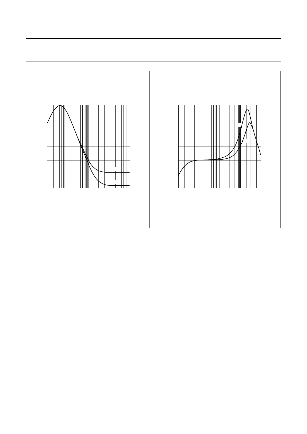
Fig.3 Typical playback frequency response.
10
LS/Fe
LS/Cr
4
f (Hz)
MLA337
LS
MLA338
HS
4
10
f (Hz)
5
10
40
handbook, halfpage
20 log [H(f)]
(dB)
30
20
5
10
10
10
2
10
3
10
Fig.4 Typical record frequency response.
April 1992 13
Page 14
Philips Semiconductors Product specification
Double-deck playback/record IC (DDPR) TDA1602A
V
O
(V)
1.65
1.5
1.35
typical
V = 1 dB typical
O
V
Osel
(V)
V
(V)
1.1
0.33
O
1.5
10
2
10
V
I right
= 300 mV
3
3.3 V
10
VI(mV)
4
10
handbook, halfpage
V
OSC
MLA340
(V)
13
= 10
V
Osel
dB
2
t (s)
3 dB
t
s
t
1
t
r
1 dB
t (s)
MLA339
0
02 13
V
control
(V)
Fig.6 Control voltage/oscillator output voltage
Fig.5 Typical ALC curve.
(V peak).
April 1992 14
Page 15
Philips Semiconductors Product specification
Double-deck playback/record IC (DDPR) TDA1602A
handbook, full pagewidth
(V)
3/4 V
1/4 V
V
8
V
P
+1
P
–1
+1
P
–1
0
channel A mute channel B channel B mute channel A
Fig.7 Channel selection input.
MLA341
t (s)
handbook, full pagewidth
V
7V,9
(V)
V
P
6.0
0.3
gradual
switch over
0
Cr02
signal
Fe02
mute
Cr02 and Fe02 = pin 9; signal and mute = pin 7
Fig.8 Tape selection input and signal/mute input.
April 1992 15
Fe02
mute
Cr02
signal
MLA343
t (s)
Page 16
Philips Semiconductors Product specification
Double-deck playback/record IC (DDPR) TDA1602A
handbook, full pagewidth
V
2/3 V
1/3 V
10
(V)
V
P
+1
P
–1
+1
P
–1
0
play record high speed
record
record
Fig.9 Playback/record/high-speed selection input.
MLA342
t (s)
playrecordhigh speed
April 1992 16
Page 17
Philips Semiconductors Product specification
Double-deck playback/record IC (DDPR) TDA1602A
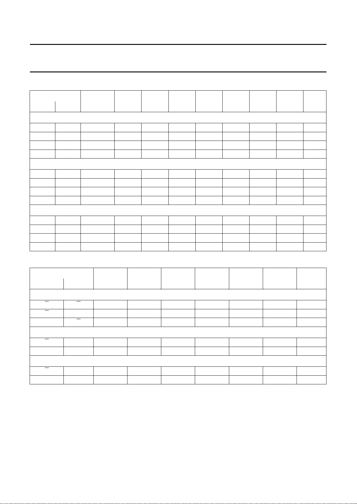
Table 1 Logic DDPR (S/M input not included)
LOGIC INPUTS CHANNEL R/P HS Fe/Cr PB DUB. REC. ALC BIAS
A/B Fe/CrA SELECT SWITCH SWITCH PB AMP. SWITCH AMP. OP. OSC.
Playback
A Fe A P ON Fe ON mute OFF OFF OFF
A Cr A P ON Cr ON mute OFF OFF OFF
B Fe B P ON Fe ON mute OFF OFF OFF
B Cr B P ON Cr ON mute OFF OFF OFF
Record
A Fe A R ON Fe ON dubbing ON OFF ON
A Cr A R ON Cr ON dubbing ON OFF ON
B Fe A R ON Fe ON line ON ON ON
B Cr A R ON Cr ON line ON ON ON
High speed record
A Fe AHS R OFF Fe ON dubbing ON OFF ON
A Cr AHS R OFF Cr ON dubbing ON OFF ON
B Fe A R ON Fe ON line ON ON ON
B Cr A R ON Cr ON line ON ON ON
Table 2 Double deck application
DECK SELECT A/B S/M CHANNEL HS PB DUB. ALC
A(P) B(R/P) INPUT INPUT SELECT SWITCH AMP. SWITCH OP.
Playback
A B don’t care M A or B OFF OFF mute OFF
A B B S B OFF ON mute OFF
A
Record
A B B M (1) A OFF OFF (1) line ON
A B A S A OFF ON dubbing OFF
High speed record
A B B M (1) A OFF OFF (1) line ON
A B A M (1) AHS ON OFF (1) dubbing OFF
Notes to Table 2
1. Fe/Cr selection not included.
2. S is also possible; play buffer = ON.
B A S A OFF ON mute OFF
April 1992 17
Page 18
Philips Semiconductors Product specification
Double-deck playback/record IC (DDPR) TDA1602A
APPLICATION INFORMATION
handbook, full pagewidth
HF bias
R4
input
HF bias
R6
input
A
(2)
Fe/CrB
Fe/CrB
R11 R12
C8
C10
S/M
Fe/Cr
R/P
VR
TDA1602A
VR
VR
OSCILLATOR
S/M
1/2
1/2
LOGIC
P/R/HSR
V
S/M
A/B
Fe/Cr
I
V
control
MLA344 - 1
C22
1
R15
V
O
C23
2
R16
V
O
C24
R24
R18
R19
S/M
A/B
Fe/CrB
P/R
C26
R17
R20
R23
R26
R25
V
I
V
OSEL
VR
V
OSEL
VR
C25
V
I
R21
LS/HS
R22
V
R
V
P
TR1
HF
output
C
27
VR
3
4
5
6
7
8
9
10
11
ref
12
ref
13
14
15
16
17
V–
18
C20 C21
R1
L
VR
R
R2
VR
(2)
VR
R9R7
C14
VR
C15
R10R8
VR
R3
L
VR
R
R5
C4
C3
C5
C11
C7
C18
38
C1
37
C2
36
35
34
33
C6
32
(1)
31
21
C12
C13
29
VTR
C16
28
C17
30
22
(1)
27
P/R
26
25
C9
24
P/R
23
LS/HS
LS/HS
AL
A
AR
LS/HS
LS/HS
BL
BR
AHS
BB
∑
BL
∑
BR
ALC
K
ALC
attack 20 19 recovery
R13
39 40
L
Fe/Cr
LS/HS
R
Fe/Cr LS/HS
R
L
LS/HS
C19 R14
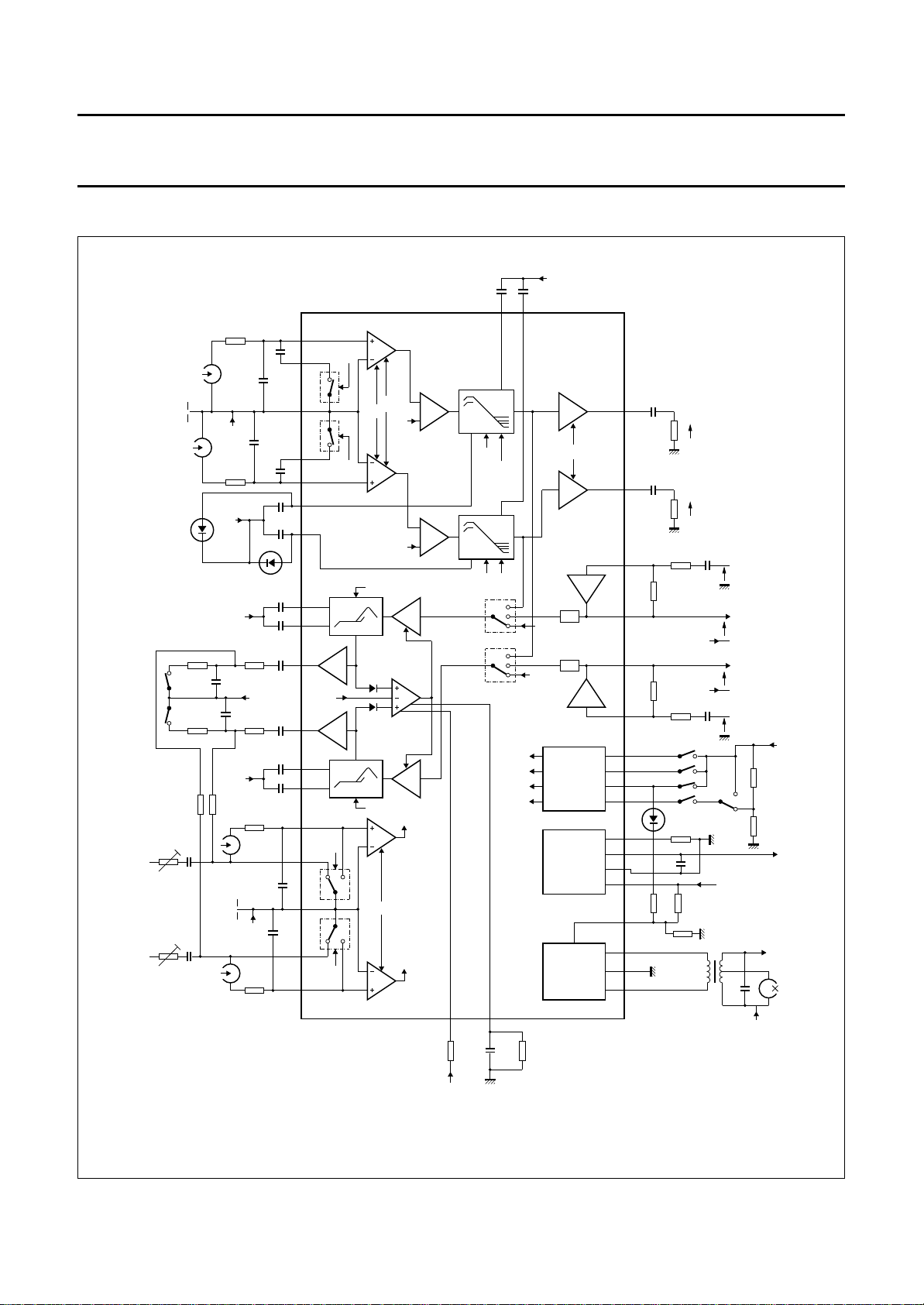
(1) Dolby application: omit C11 and C18.
(2) Required for low voltage application VP< 12 V.
April 1992 18
Fig.10 Application diagram.
Page 19
Philips Semiconductors Product specification
Double-deck playback/record IC (DDPR) TDA1602A
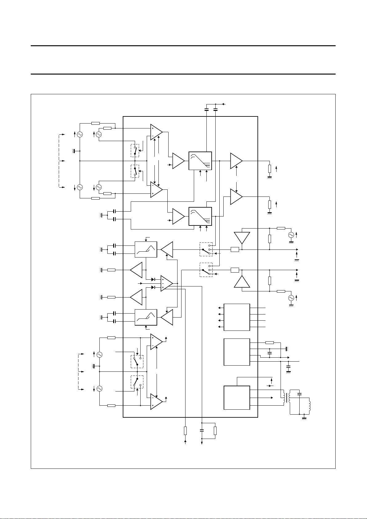
TEST INFORMATION
handbook, full pagewidth
V
L
A
R
V
VR
R
S
V
LS
V
LS
L
B
R
R
HS
HS
R
R
S
V
I
V
I
38
S
37
36
35
S
34
33
32
31
21
R
LA
29
VTR
R
LA
28
30
22
R
S
27
P/R
26
25
24
R
S
P/R
23
LS/HS
LS/HS
AL
A
AR
LS/HS
LS/HS
BL
BR
B
AHS
∑
BL
∑
BR
ALC
K
ALC
attack 20 19 recovery
R
V
L
Fe/Cr
R
Fe/Cr LS/HS
R
L
a
P
LS/HS
C
V–
39 40
S/M
Fe/Cr
LS/HS
R/P
r
TDA1602A
VR
VR
OSCILLATOR
R
r
S/M
1/2
1/2
LOGIC
P/R/HSR
V
S/M
A/B
Fe/Cr
I
V
control
V–
ref
ref
10
11
12
13
14
15
16
17
18
MLA345
1
R
L
V
O
2
R
L
V
O
R
3
4
5
6
7
8
9
V–
I
V
TR1
I
V
OSEL
V
OSEL
V
I
V
R
V–
R
t
R
t
R
I
R
ref
V
C
V–
April 1992 19
Fig.11 Test circuit diagram.
Page 20

Philips Semiconductors Product specification
Double-deck playback/record IC (DDPR) TDA1602A
Table 3 Component values used in the application diagram
COMPONENT CONDITION VALUE UNIT
Resistors
R1, R2 47 Ω
R3, R5 47 Ω
R4, R6 potentiometer 47 kΩ
R7, R8 tbf
R9, R10 6.8 kΩ
R11, R12 8.2 kΩ
R13 100 Ω
R14 1MΩ
R15, R16 100 kΩ
R17, R20 tbf
R18, R19 tbf
R21, R22 10 kΩ
R23 2kΩ
R24, R25, R26 5.1 kΩ
Capacitors
C1, C4 330 pF
C2, C3 330 pF
C5, C6 47 nF
C7, C9 680 pF
C8, C10 820 pF
C11, C18 68 nF
C12, C17 100 µF
C13, C16 4.7 µF
C14, C15 tbf
C19 47 µF
C20, C21 100 nF
C22, C23 4.7 µF
C24, C25 4.7 µF
C26 100 µF
C27 3.9 nF
April 1992 20
Page 21

Philips Semiconductors Product specification
Double-deck playback/record IC (DDPR) TDA1602A
Table 4 Component values used in the test circuit
COMPONENT CONDITION VALUE UNIT
Resistors
R
S
R
L
R
LA
R
I
R
t
R
ref
R
a
R
r
Capacitors
C
r
1kΩ
100 kΩ
10 kΩ
4.7 kΩ
22.6 kΩ
2kΩ
1kΩ
3.3 MΩ
1 µF
April 1992 21
Page 22
Philips Semiconductors Product specification
Double-deck playback/record IC (DDPR) TDA1602A
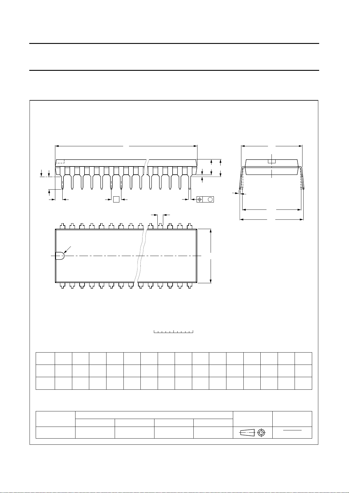
PACKAGE OUTLINE
DIP40: plastic dual in-line package; 40 leads (600 mil)
D
seating plane
L
Z
40
pin 1 index
e
b
SOT129-1
M
E
A
2
A
A
1
w M
b
1
21
E
c
(e )
1
M
H
1
0 5 10 mm
scale
DIMENSIONS (inch dimensions are derived from the original mm dimensions)
A
A
A
UNIT
inches
Note
1. Plastic or metal protrusions of 0.25 mm maximum per side are not included.
max.
mm
OUTLINE
VERSION
SOT129-1
1 2
min.
max.
1.70
1.14
0.067
0.045
IEC JEDEC EIAJ
051G08 MO-015AJ
b
b
1
0.53
0.38
0.021
0.015
0.36
0.23
0.014
0.009
REFERENCES
cD E e M
52.50
51.50
2.067
2.028
April 1992 22
14.1
13.7
0.56
0.54
20
(1)(1)
e
L
1
3.60
3.05
0.14
0.12
M
E
15.80
15.24
0.62
0.60
EUROPEAN
PROJECTION
17.42
15.90
0.69
0.63
H
w
0.2542.54 15.24
0.010.10 0.60
ISSUE DATE
92-11-17
95-01-14
max.
2.254.7 0.51 4.0
0.089 0.19 0.020 0.16
(1)
Z
Page 23

Philips Semiconductors Product specification
Double-deck playback/record IC (DDPR) TDA1602A
SOLDERING
Introduction
There is no soldering method that is ideal for all IC
packages. Wave soldering is often preferred when
through-hole and surface mounted components are mixed
on one printed-circuit board. However, wave soldering is
not always suitable for surface mounted ICs, or for
printed-circuits with high population densities. In these
situations reflow soldering is often used.
This text gives a very brief insight to a complex technology.
A more in-depth account of soldering ICs can be found in
“IC Package Databook”
our
Soldering by dipping or by wave
The maximum permissible temperature of the solder is
260 °C; solder at this temperature must not be in contact
with the joint for more than 5 seconds. The total contact
time of successive solder waves must not exceed
5 seconds.
DEFINITIONS
(order code 9398 652 90011).
The device may be mounted up to the seating plane, but
the temperature of the plastic body must not exceed the
specified maximum storage temperature (T
printed-circuit board has been pre-heated, forced cooling
may be necessary immediately after soldering to keep the
temperature within the permissible limit.
Repairing soldered joints
Apply a low voltage soldering iron (less than 24 V) to the
lead(s) of the package, below the seating plane or not
more than 2 mm above it. If the temperature of the
soldering iron bit is less than 300 °C it may remain in
contact for up to 10 seconds. If the bit temperature is
between 300 and 400 °C, contact may be up to 5 seconds.
stg max
). If the
Data sheet status
Objective specification This data sheet contains target or goal specifications for product development.
Preliminary specification This data sheet contains preliminary data; supplementary data may be published later.
Product specification This data sheet contains final product specifications.
Limiting values
Limiting values given are in accordance with the Absolute Maximum Rating System (IEC 134). Stress above one or
more of the limiting values may cause permanent damage to the device. These are stress ratings only and operation
of the device at these or at any other conditions above those given in the Characteristics sections of the specification
is not implied. Exposure to limiting values for extended periods may affect device reliability.
Application information
Where application information is given, it is advisory and does not form part of the specification.
LIFE SUPPORT APPLICATIONS
These products are not designed for use in life support appliances, devices, or systems where malfunction of these
products can reasonably be expected to result in personal injury. Philips customers using or selling these products for
use in such applications do so at their own risk and agree to fully indemnify Philips for any damages resulting from such
improper use or sale.
April 1992 23
 Loading...