

Page 1

INTEGRATED CIRCUITS
DATA SH EET
TDA1575T
FM front end circuit for CENELEC
EN 55020 applications
Preliminary specification
File under Integrated Circuits, IC01
April 1993
Page 2

Philips Semiconductors Preliminary specification
FM front end circuit for CENELEC EN
TDA1575T
55020 applications
FEATURES
• Bipolar integrated FM front end circuit, designed for use
in car radios and home receivers
• Fulfills CENELEC EN 55020 requirements
• Radio frequency range of 76 to 90 MHz (Japan) or 87.5
to 108 MHz (Europe, USA)
• Low noise oscillator, buffered oscillator output
• Double balanced mixer
• Internal buffered mixer driving
• Linear IF amplifier, suitable for ceramic IF filters
• Regulated reference voltage.
QUICK REFERENCE DATA
SYMBOL PARAMETER MIN. TYP. MAX. UNIT
V
P
I
P
V
REF
Z
I
NF noise figure of mixer − 9 − dB
EMF1 3rd order intermodulation − 115 − dBµV
V
OSC
THD total harmonic distortion −−15 − dBC
G
v
NF IF noise figure − 6.5 − dB
Z
I
Z
O
EMF2 AGC wideband threshold (RMS value) − 17 − mV
supply voltage 7 8.5 10 V
supply current, without mixer − 23 − mA
reference voltage output − 4.2 − V
mixer input impedance − 14 −Ω
oscillator buffer output signal (RMS value) 75 −−mV
IF gain − 30 − dB
IF input impedance − 300 −Ω
IF output impedance − 300 −Ω
ORDERING INFORMATION
EXTENDED
TYPE NUMBER
TDA1575T 16 mini-pack plastic SOT109A
Note
1. SOT109-1; 1996 August 29.
April 1993 2
PACKAGE
PINS PIN POSITION MATERIAL CODE
(1)
Page 3
Philips Semiconductors Preliminary specification
FM front end circuit for CENELEC EN
55020 applications
TDA1575T
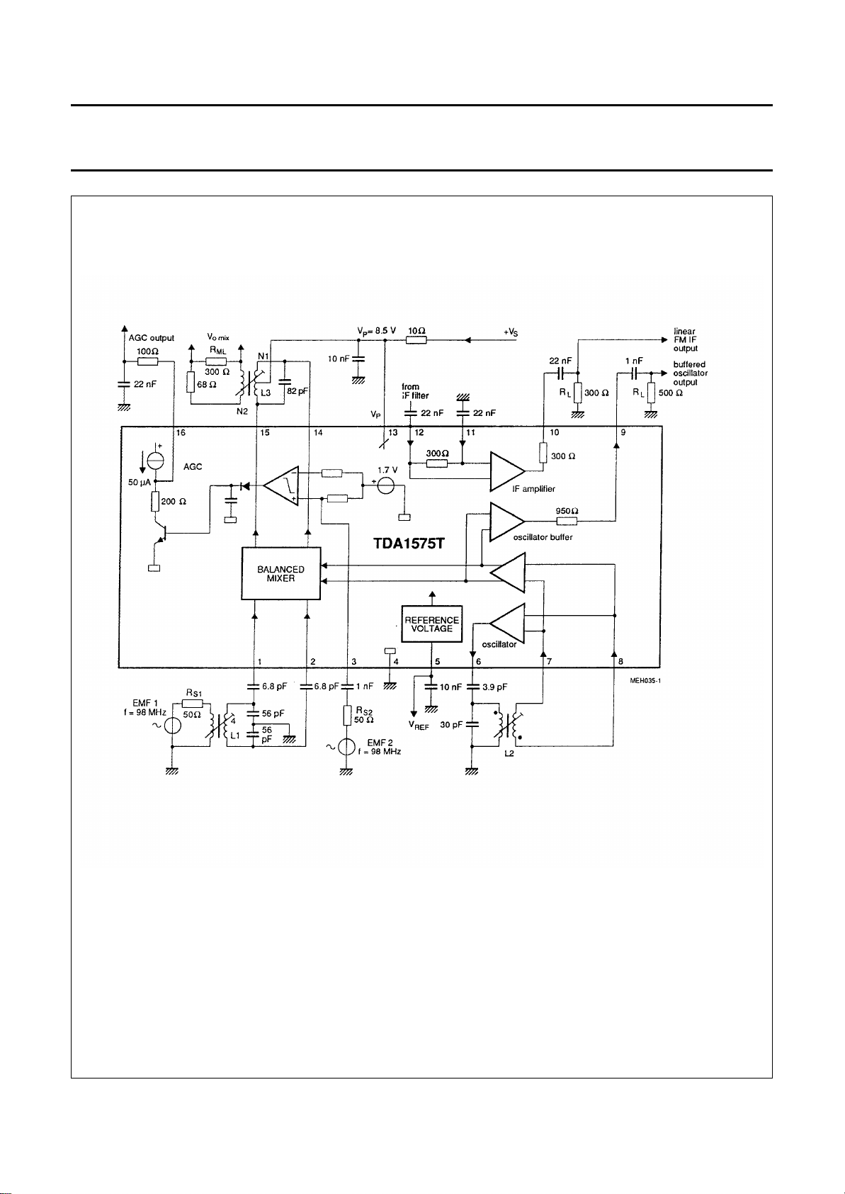
Coils TOKO
L1: MC-108 514 HNE-150023S14; L = 78 nH, N = 4 turns
L2: MC-111 E516 HNS-200057; L = 80 nH
L3: A119 ACS-17114 FTT
April 1993 3
Fig.1 Block diagram and test circuit.
Page 4
Philips Semiconductors Preliminary specification
FM front end circuit for CENELEC EN
55020 applications
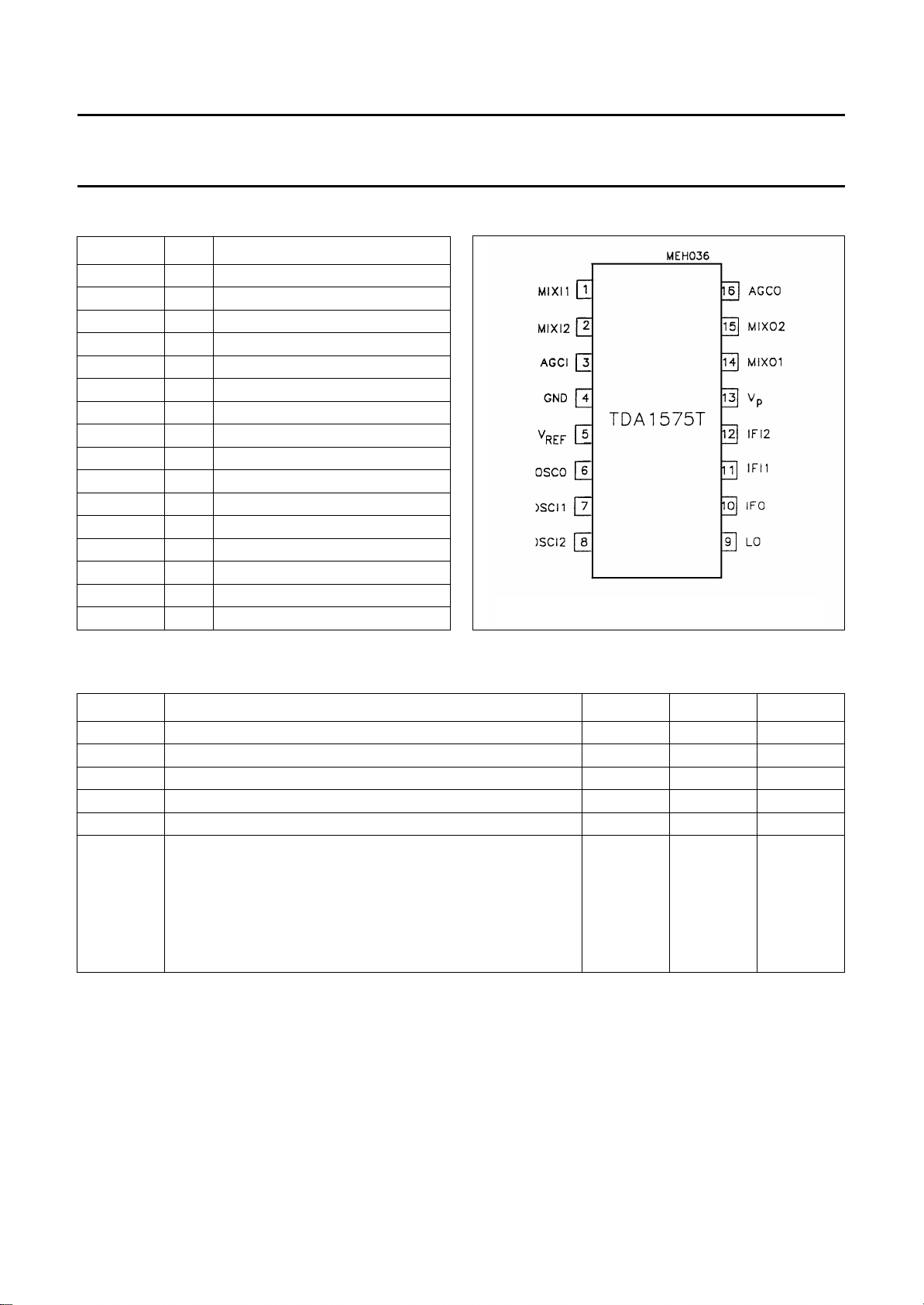
PINNING
SYMBOL PIN DESCRIPTION
MIXI1 1 RF input 1 to mixer
MIXI2 2 RF input 2 to mixer
AGCI 3 HF input to automatic gain control
GND 4 ground (0 V)
V
REF
OSCO 6 oscillator output
OSCI1 7 oscillator input 1
OSCI2 8 oscillator input 2
LO 9 buffered oscillator output
IFO 10 linear FM IF output
IFI1 11 FM IF input 1
IFI2 12 FM IF input 2
V
P
MIXO1 14 mixer output 1
MIXO2 15 mixer output 2
AGCO 16 automatic gain control output
5 reference voltage output
13 supply voltage (+8.5 V)
TDA1575T
Fig.2 Pin configuration.
LIMITING VALUES
Limiting values in accordance with the Absolute Maximum System (IEC 134).
SYMBOL PARAMETER MIN. MAX. UNIT
V
V
P
T
T
V
P
14, 15
tot
stg
amb
ESD
supply voltage (pin 13) 0 12 V
voltage at mixer output 0 V
P
V
total power dissipation 0 380 mW
storage temperature range −55 +150 °C
operating ambient temperature range −40 +85 °C
electrostatic handling (see note 1)
all pins except 3 and 10 −±2000 V
pin 3 − +2000 V
−−1000 V
pin 10 − +1500 V
−−2000 V
Note to the limiting values
1. Equivalent to discharging a 100 pF capacitor through a 1.5 kΩ series resistor.
April 1993 4
Page 5

Philips Semiconductors Preliminary specification
FM front end circuit for CENELEC EN
TDA1575T
55020 applications
CHARACTERISTICS
= 8.5 V and T
V
P
SYMBOL PARAMETER CONDITIONS MIN. TYP. MAX. UNIT
V
P
I
P
V
REF
Mixer; EMF1 = 98 MHz
I
14 + 15
V
1, 2
Z
1, 2
V
14, 15
C
14, 15
G
P
EMF1
IP3
NF noise figure − 9 − dB
= +25°C, measurements taken in Fig.1 with f0 = 98 MHz (EMF1) unless otherwise specified.
amb
supply voltage (pin 13) 7 8.5 10 V
supply current without mixer 16 23 30 mA
reference voltage (pin 5) I5 ≤ 3 mA 3.9 4.2 4.4 V
mixer supply current (pins 14 and 15) − 4 − mA
DC voltage input (pins 1 and 2) − 1 − V
input impedance − 14 −Ω
DC output voltage (pins 14 and 15) 4 − 10 V
output capacitance − 13 − pF
conversion power gain note 1 − 14 − dB
3rd order intercept point − 115 − dBµV
total noise figure including
− 11 − dB
transforming network
Oscillator; f
V
7, 8
V
6
∆f residual FM at pin 6 f = 300 to 15000 Hz;
= 108.7 MHz
OSC
DC input voltage (pins 7 and 8) − 1.3 − V
DC output voltage (pin 6) − 2.0 − V
− 2.2 − Hz
de-emphasis 50 µs
Oscillator buffered output (pin 9)
V
O
V
9
R
9
output signal (RMS value) RL= 500 Ω; CL= 2 pF 75 −−mV
DC output voltage − 6 − V
DC output resistor − 950 −Ω
THD total harmonic distortion −−15 − dBC
f
S
spurious frequencies EMF1 = 2 V;
−−37 − dBC
RS= 50 Ω;
f
= 108.7 MHz
OSC
Automatic gain control (AGC); f
R
3
C
3
V
16
I
16
input resistance (pin 3) − 4 − kΩ
input capacitance − 3 − pF
AGC output swing (DC) Figs 3 and 4 0.5 − VP − 0.3 V
output current at I3 = 0 V16 = 1/2 V
output current at U
EMF2 threshold (RMS value) I
= 98 MHz
i
P
= 2 V V16 = 7 to 10 V 2 − 5mA
3
= 0; V16 = 1/2 VP;
16
−25 −50 −150 µA
− 17 − mV
Figs 4 and 5
April 1993 5
Page 6
Philips Semiconductors Preliminary specification
FM front end circuit for CENELEC EN
TDA1575T
55020 applications
SYMBOL PARAMETER CONDITIONS MIN. TYP. MAX. UNIT
Linear IF amplifier; IF = 10.7 MHz
V
11, 12
Z
12-11
C
12-11
V
10
Z
10
C
10
V
O
G
v
∆G
v
NF noise figure R
Note
1. GP = 10 log (4V
DC input voltage (pins 11 and 12) − 1.25 − V
input impedance 240 300 360 Ω
input capacitance − 13 − pF
DC output voltage (pin 10) − 4.4 − V
output impedance 240 300 360 Ω
output capacitance − 3 − pF
output signal (RMS value) −1 dB compression −−650 mV
IF voltage gain (20 log (V
IF voltage gain deviation T
×10.7 MHz) / (EMF2 × 98 MHz)2 × (RS1 / RML).
o mix
10−4
/ V
)) 27 30 − dB
12−11
= −40 to +85 °C − 0 − dB
amb
= 300 Ω−6.5 − dB
S
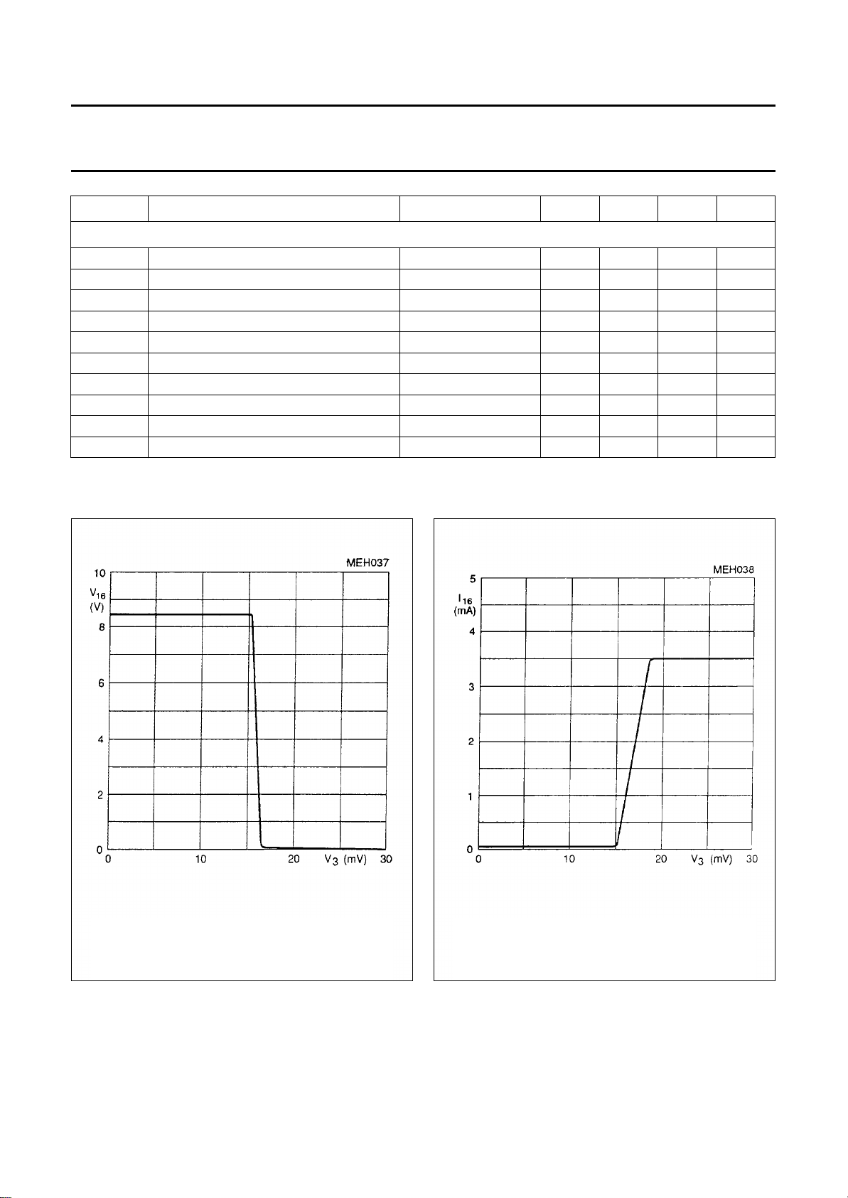
Fig.3 AGC output voltage V16 as a function of V
RMS at I16 = 0, measured in test circuit
Fig.1.
April 1993 6
i3
Fig.4 AGC output current I16 as a function of V
i3
RMS at V16 = 8.5 V, measured in test circuit
Fig.1.
Page 7
Philips Semiconductors Preliminary specification
FM front end circuit for CENELEC EN
TDA1575T
55020 applications
APPLICATION INFORMATION
Operating characteristics
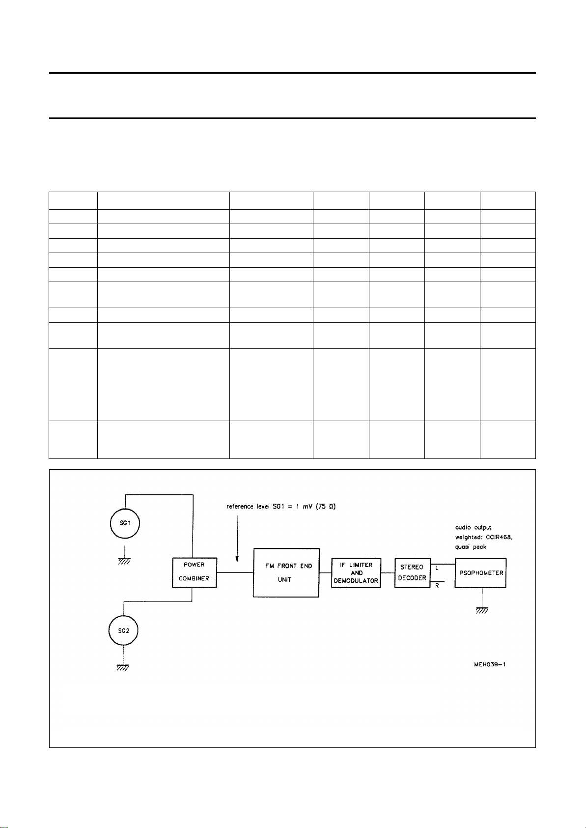
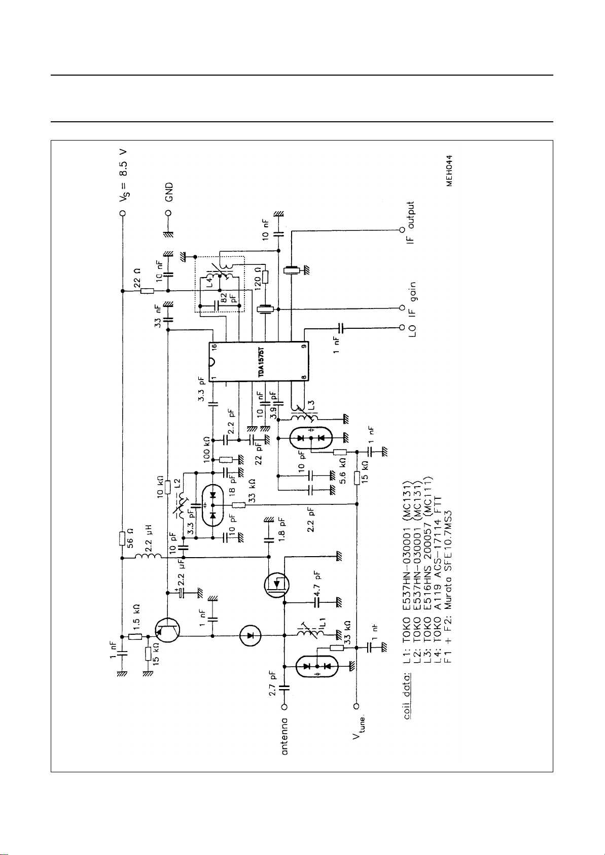
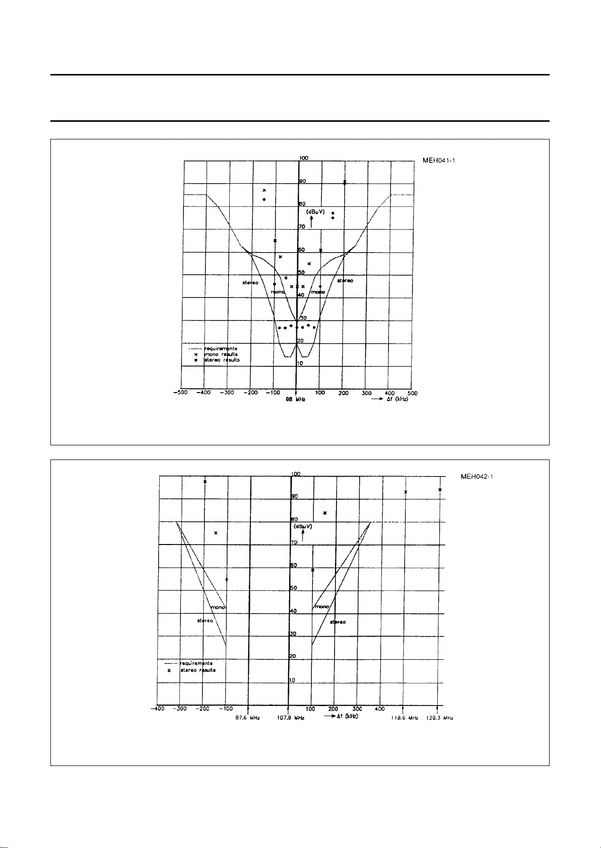
Measured in application circuit Fig.7, according to CENELEC EN 55020, Chapter 4.1 (passive interference
suppression). Measurements are shown in Figs. 8 and 9.
SYMBOL PARAMETER CONDITIONS MIN. TYP. MAX. UNIT
V
S
I
S
f
RF
V
tune
G gain (20 log V
V
i ant
IR image rejection f = 98 MHz − 64 − dB
RSS repeat spot suppression f = 98 MHz;
DBS double beat suppression f1 = 93 MHz;
CBS continuous beat suppression f1 = 90 MHz;
supply voltage 7 8.5 10 V
total supply current − 37 − mA
tuning range of RF input 87.5 − 108 MHz
tuning voltage of RF input 1 − 7V
/ V
O IF
input sensitivity S/N = 26 dB;
) − 43 − dB
ant
− 2 −µV
R
= 150 Ω
ant
− 89 − dB
= 10 µV
V
i ant
f2 = 98 MHz
DBS1 f
DBS2 f
DBS3 f
= 88 MHz − 81 − dB
tune
= 103 MHz − 80 − dB
tune
= 90.15 MHz − 85 − dB
tune
− 90 − dB
f2 = 100.7 MHz
= 95 MHz
f
tune
SG1: Wanted carrier; modulated with f = 1 kHz, ∆f =±40 kHz (for audio reference)
SG2: Unwanted carrier; modulated with f = 1 kHz, FM: ∆f =±40 kHz (in band) or AM: m = 80% (out of band)
increase level of SG2 until S/N = 26 dB w.r.t. wanted modulation (for car radio, home radio S/N = 40 dB)
April 1993 7
Fig.5 Set-up for CENELEC EN 55020 passive interference measurements.
Page 8
Philips Semiconductors Preliminary specification
FM front end circuit for CENELEC EN
55020 applications
TDA1575T
April 1993 8
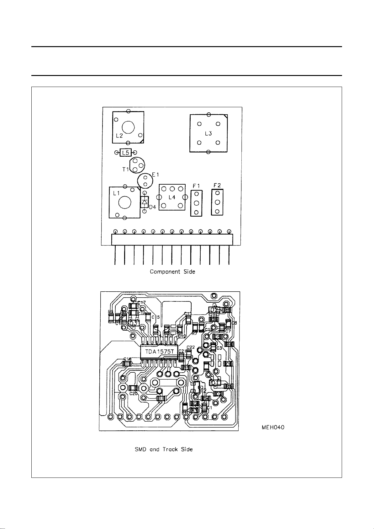
Fig.6 PCB layout of FM front end unit.
Page 9
Philips Semiconductors Preliminary specification
FM front end circuit for CENELEC EN
55020 applications
TDA1575T
April 1993 9
Fig.7 Application circuit of FM front end with TDA1575Tand FET-preamplifier.
Page 10
Philips Semiconductors Preliminary specification
FM front end circuit for CENELEC EN
55020 applications
TDA1575T
Fig.8 Interference level as a function of detuning for S/N = 26 dB; IN-BAND passive interference (CENELEC EN
55020).
Fig.9 Interference level as a function of detuning for S/N = 26 dB; OUT-OF-BAND passive interference
(CENELEC EN 55020).
April 1993 10
Page 11
Philips Semiconductors Preliminary specification
FM front end circuit for CENELEC EN
55020 applications
TDA1575T
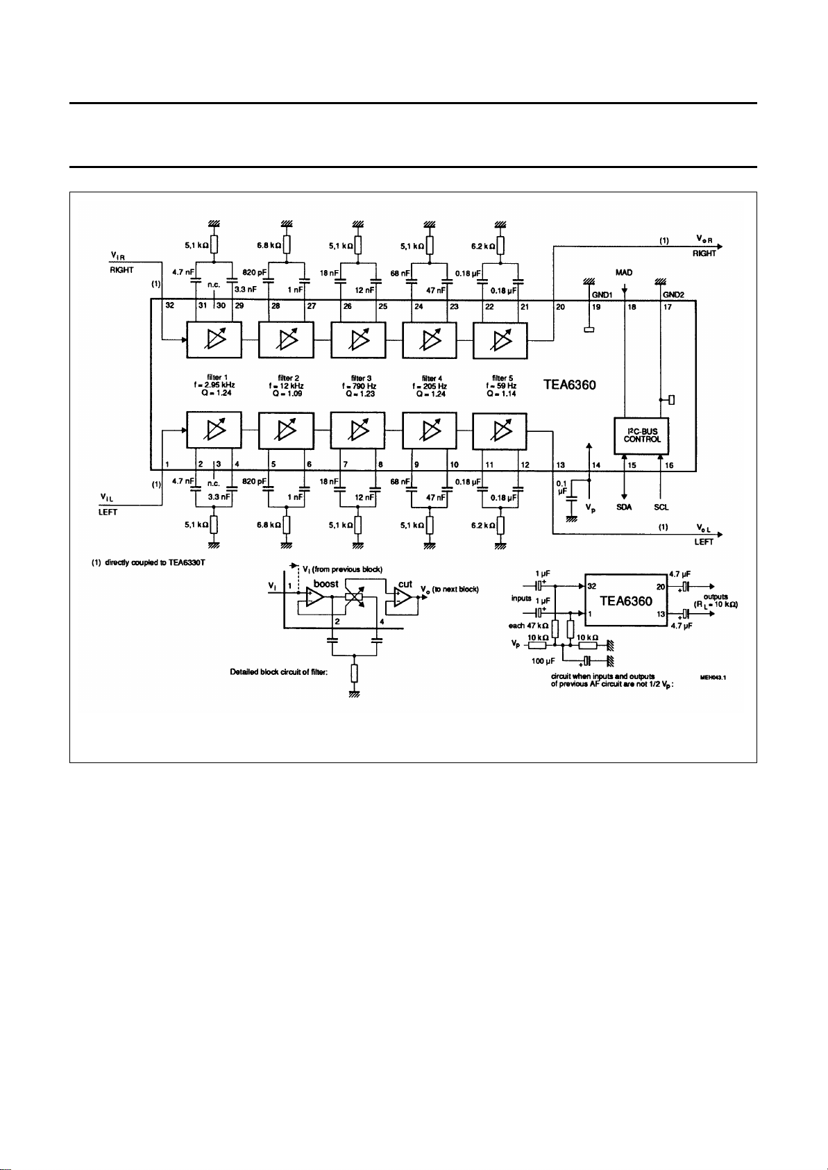
Fig.10 Internal circuits.
April 1993 11
Page 12
Philips Semiconductors Preliminary specification
FM front end circuit for CENELEC EN
55020 applications
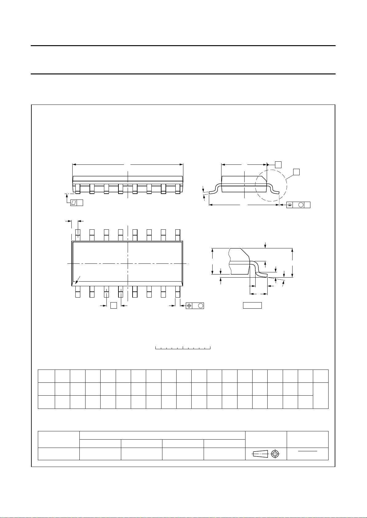
PACKAGE OUTLINE
SO16: plastic small outline package; 16 leads; body width 3.9 mm
D
c
y
Z
16
9
TDA1575T
SOT109-1
E
H
E
A
X
v M
A
pin 1 index
1
e
0 2.5 5 mm
DIMENSIONS (inch dimensions are derived from the original mm dimensions)
mm
A
max.
1.75
0.069
A1A2A
0.25
1.45
0.10
1.25
0.0098
0.057
0.0039
0.049
0.25
0.01
b
3
p
0.49
0.25
0.36
0.19
0.0098
0.019
0.0075
0.014
UNIT
inches
Note
1. Plastic or metal protrusions of 0.15 mm maximum per side are not included.
(1)E(1) (1)
cD
10.0
9.8
0.39
0.38
8
b
p
scale
eHELLpQZywv θ
4.0
1.27
3.8
0.16
0.050
0.15
w M
6.2
5.8
0.24
0.23
A
2
1.05
0.041
Q
A
1
detail X
1.0
0.7
0.4
0.6
0.028
0.039
0.020
0.016
(A )
L
p
L
0.25 0.1
0.25
0.01
0.01 0.004
A
3
θ
0.7
0.3
0.028
0.012
o
8
o
0
OUTLINE
VERSION
SOT109-1
April 1993 12
REFERENCES
IEC JEDEC EIAJ
076E07S MS-012AC
EUROPEAN
PROJECTION
ISSUE DATE
91-08-13
95-01-23
Page 13

Philips Semiconductors Preliminary specification
FM front end circuit for CENELEC EN
55020 applications
SOLDERING
Introduction
There is no soldering method that is ideal for all IC
packages. Wave soldering is often preferred when
through-hole and surface mounted components are mixed
on one printed-circuit board. However, wave soldering is
not always suitable for surface mounted ICs, or for
printed-circuits with high population densities. In these
situations reflow soldering is often used.
This text gives a very brief insight to a complex technology.
A more in-depth account of soldering ICs can be found in
“IC Package Databook”
our
Reflow soldering
Reflow soldering techniques are suitable for all SO
packages.
Reflow soldering requires solder paste (a suspension of
fine solder particles, flux and binding agent) to be applied
to the printed-circuit board by screen printing, stencilling or
pressure-syringe dispensing before package placement.
Several techniques exist for reflowing; for example,
thermal conduction by heated belt. Dwell times vary
between 50 and 300 seconds depending on heating
method. Typical reflow temperatures range from
215 to 250 °C.
Preheating is necessary to dry the paste and evaporate
the binding agent. Preheating duration: 45 minutes at
45 °C.
(order code 9398 652 90011).
TDA1575T
Wave soldering
Wave soldering techniques can be used for all SO
packages if the following conditions are observed:
• A double-wave (a turbulent wave with high upward
pressure followed by a smooth laminar wave) soldering
technique should be used.
• The longitudinal axis of the package footprint must be
parallel to the solder flow.
• The package footprint must incorporate solder thieves at
the downstream end.
During placement and before soldering, the package must
be fixed with a droplet of adhesive. The adhesive can be
applied by screen printing, pin transfer or syringe
dispensing. The package can be soldered after the
adhesive is cured.
Maximum permissible solder temperature is 260 °C, and
maximum duration of package immersion in solder is
10 seconds, if cooled to less than 150 °C within
6 seconds. Typical dwell time is 4 seconds at 250 °C.
A mildly-activated flux will eliminate the need for removal
of corrosive residues in most applications.
Repairing soldered joints
Fix the component by first soldering two diagonallyopposite end leads. Use only a low voltage soldering iron
(less than 24 V) applied to the flat part of the lead. Contact
time must be limited to 10 seconds at up to 300 °C. When
using a dedicated tool, all other leads can be soldered in
one operation within 2 to 5 seconds between
270 and 320 °C.
April 1993 13
Page 14

Philips Semiconductors Preliminary specification
FM front end circuit for CENELEC EN
TDA1575T
55020 applications
DEFINITIONS
Data sheet status
Objective specification This data sheet contains target or goal specifications for product development.
Preliminary specification This data sheet contains preliminary data; supplementary data may be published later.
Product specification This data sheet contains final product specifications.
Limiting values
Limiting values given are in accordance with the Absolute Maximum Rating System (IEC 134). Stress above one or
more of the limiting values may cause permanent damage to the device. These are stress ratings only and operation
of the device at these or at any other conditions above those given in the Characteristics sections of the specification
is not implied. Exposure to limiting values for extended periods may affect device reliability.
Application information
Where application information is given, it is advisory and does not form part of the specification.
LIFE SUPPORT APPLICATIONS
These products are not designed for use in life support appliances, devices, or systems where malfunction of these
products can reasonably be expected to result in personal injury. Philips customers using or selling these products for
use in such applications do so at their own risk and agree to fully indemnify Philips for any damages resulting from such
improper use or sale.
April 1993 14
 Loading...