

Page 1
INTEGRATED CIRCUITS
DATA SH EET
TDA1545A
Stereo continuous calibration DAC
Preliminary specification
File under Integrated Circuits, IC01
March 1993
Page 2
Philips Semiconductors Preliminary specification
Stereo continuous calibration DAC TDA1545A
FEATURES
• Space saving package (SO8 or DIL8)
• Low power consumption
• Low total harmonic distortion
• Wide dynamic range (16-bit resolution)
• Continuous calibration concept
• Easy application: single 3 to 5.5 V rail power supply and
output- and bias current are proportional to the supply
voltage
• Fast settling time permits 2 ×, 4 × and 8 × oversampling
(serial input) or double speed operation at 4 ×
oversampling
• Internal bias current ensures maximum dynamic range
• Wide operating temperature range of −40 °C to +85 °C
• Compatible with most of the Japanese input formats:
time multiplexed, two's complement and TTL
• No zero crossing distortion.
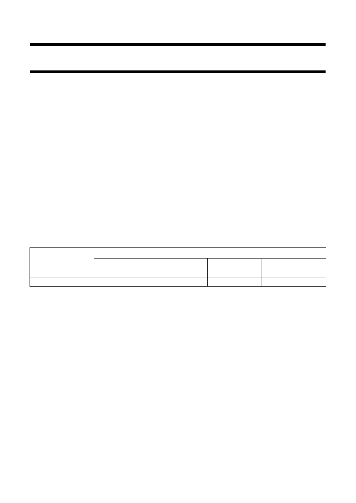
ORDERING INFORMATION
EXTENDED TYPE
NUMBER
TDA1545A
TDA1545AT
(1)
(2)
PINS PIN POSITION MATERIAL CODE
8 DIL plastic SOT97
8 mini-pack plastic SO8; SOT96A
GENERAL DESCRIPTION
The TDA1545A is the first device of a new generation of
the digital-to-analog convertors which embodies the
innovative technique of continuous calibration. The largest
bit-currents are repeatedly generated by one single
current reference source. This duplication is based upon
an internal charge storage principle having an accuracy
insensitive to ageing, temperature and process variations.
The device is fabricated in a 1.0 µm CMOS process and
features an extremely low power dissipation, small
package size and easy application. Furthermore, the
accuracy of the high coarse current combined with the
implemented symmetrical offset decoding method
preclude zero-crossing distortion and ensures high quality
audio reproduction. Therefore, the continuous calibration
digital-to-analog convertor is eminently suitable for use in
(portable) digital audio equipment.
PACKAGE
Notes
1. SOT97-1; 1996 August 19.
2. SOT96-1; 1996 August 19.
March 1993 2
Page 3
Philips Semiconductors Preliminary specification
Stereo continuous calibration DAC TDA1545A
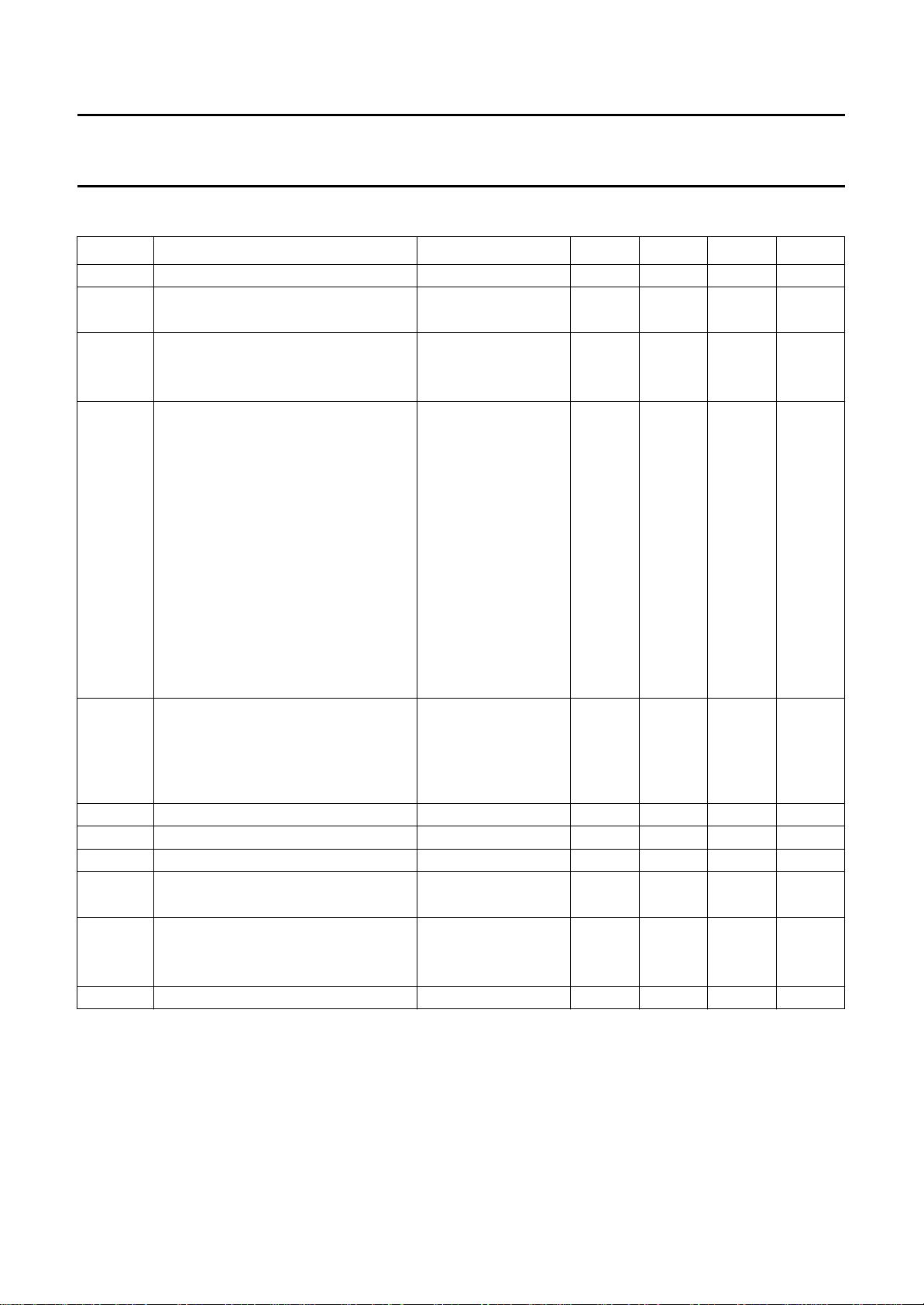
QUICK REFERENCE DATA
SYMBOL PARAMETER CONDITIONS MIN. TYP. MAX. UNIT
V
DD
I
DD
I
FS
THD total harmonic distortion including noise
S/N signal-to-noise ratio at bipolar zero
t
cs
BR input bit rate at data input −−18.4 Mbits/s
f
BCK
TC
FS
P
tot
T
amb
supply voltage 3 5 5.5 V
supply current VDD = 5 V; − 3.0 4.0 mA
at code 0000H
full scale output current
= 5 V 0.9 1.0 1.1 mA
V
DD
= 3 V − 0.6 − mA
V
DD
at 0 dB −−88 −78 dB
at 0 dB − 0.004 0.01 %
at −60 dB −−33 −24 dB
at −60 dB − 2.2 6 %
at −60 dB; −−35 − dB
A-weighting
at −60 dB; − 1.7 − %
A-weighting
at −60 dB; − 1.4 − %
A-weighting;
R3 = R4 = 11 kΩ;
= 2 mA
I
FS
A-weighting;
86 98 − dB
at code 0000H
R3 = R4 = 11 kΩ;
= 2 mA
I
FS
− 101 − dB
current settling time to ±1 LSB − 0.2 −µs
clock frequency at clock input −−18.4 MHz
full scale temperature coefficient −±400 − ppm
at analog outputs (IOL; IOR)
total power dissipation at code 0000H
= 5 V − 15 20 mW
V
DD
= 3 V − 6 − mW
V
DD
operating ambient temperature −40 − +85 °C
March 1993 3
Page 4
Philips Semiconductors Preliminary specification
Stereo continuous calibration DAC TDA1545A
C4
1 nF
C1
out
left
V
C2
OP1
R1
3.9 kΩ
IOL
6
BL
I
V
1 nF
REF
out
right
V
OP2
R2
3.9 kΩ
REF
V
IOR
8
BR
I
REF
DIVIDER
I
11-BIT
PASSIVE
I
I
I
V
BR
REF
BL
REF
R4
(E24)
33 kΩ
7
REF
I
SOURCE
REFERENCE
1 µF
R3
R
(E24)
REF
DD
22 kΩ
11 kΩ
V
C3
100 nF
ground
5
4
MCD287 - 1
handbook, full pagewidth
RIGHT OUTPUT LATCH
LEFT OUTPUT LATCH
RIGHT BIT SWITCHES
LEFT BIT SWITCHES
32 (5-BIT)
CURRENT
SOURCES
CALIBRATED
32 (5-BIT)
CURRENT
SOURCES
CALIBRATED
11-BIT
DIVIDER
PASSIVE
&
SPARE
SOURCE
1 CALIBRATED
&
SPARE
SOURCE
1 CALIBRATED
REF
I
LEFT INPUT LATCH
RIGHT INPUT LATCH
TDA1545A
&
TIMING
CONTROL
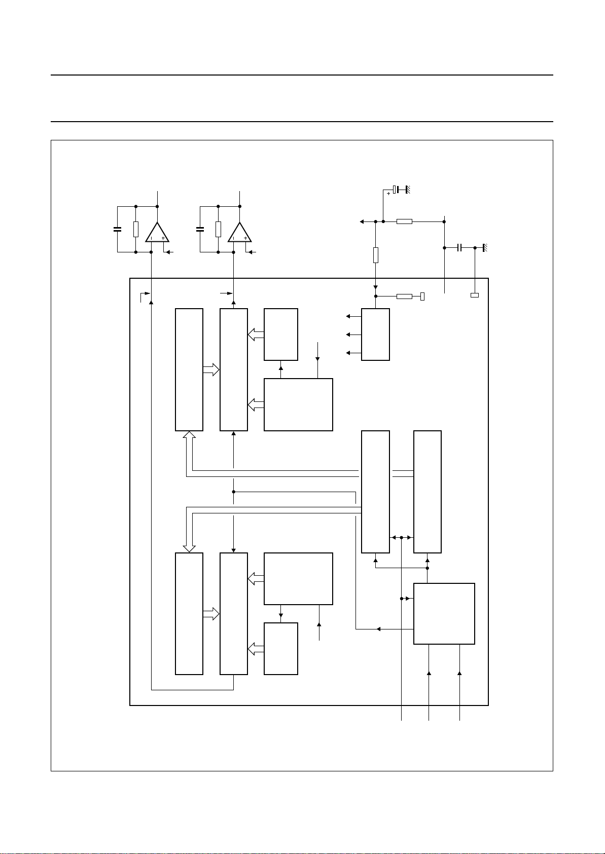
Fig.1 Block diagram.
March 1993 4
1
BCK
2
3
WS
DATA
Page 5
Philips Semiconductors Preliminary specification
Stereo continuous calibration DAC TDA1545A
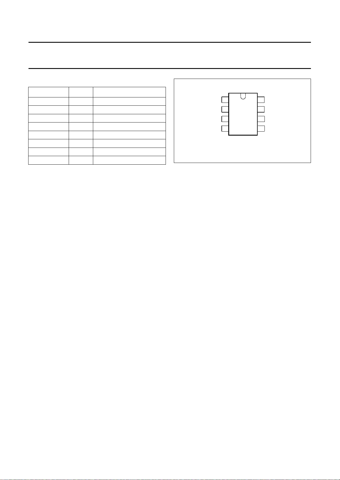
PINNING
SYMBOL PIN DESCRIPTION
BCK 1 bit clock input
WS 2 word select input
DATA 3 data input
GND 4 ground
V
DD
5 positive supply voltage
IOL 6 left channel output
I
REF
7 reference current input
IOR 8 right channel output
handbook, halfpage
1
BCK
2
WS
DATA
GND
TDA1545A
3
4
MCD288 - 1
Fig.2 Pin configuration.
8
IOR
I
7
REF
IOL
6
V
5
DD
March 1993 5
Page 6
Philips Semiconductors Preliminary specification
Stereo continuous calibration DAC TDA1545A
FUNCTIONAL DESCRIPTION
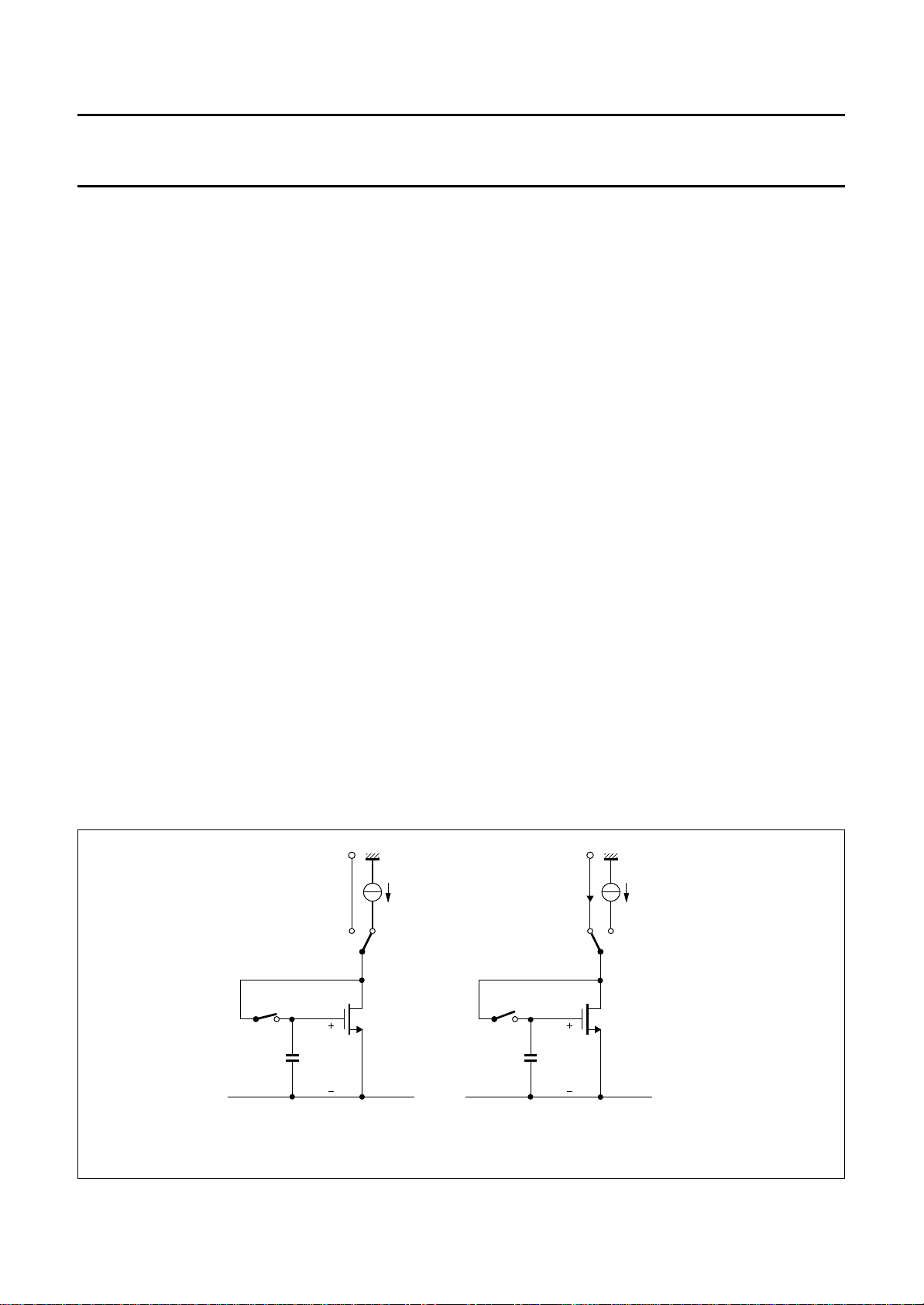
The basic operation of the continuous calibration DAC is
illustrated in Fig.3. The figure shows the calibration
principle (Fig.3a) and operation principle (Fig.3b). During
calibration of the MOS current source (Fig.3a) transistor
M1 is connected as a diode by applying a reference
current. The voltage Vgs on the intrinsic gate-source
capacitance Cgs of M1 is then determined by the transistor
characteristics. After calibration of the drain current to the
reference value I
, the switch S1 is opened and S2 is
REF
switched to the other position (Fig.3b). The gate-to-source
voltage Vgs of M1 is not changed because the charge on
Cgs is preserved. Therefore the drain current of M1 will still
be equal to I
available at the I
and this exact duplicate of I
REF
terminal. The 32 current sources and
out
REF
is now
the spare current source of the TDA1545A are
continuously calibrated (see Fig.1). The spare current is
included to allow for continuous convertor operation. The
output of one calibrated source is connected to an 11-bit
binary current divider consisting of 2048 transistors. A
symmetrical offset decoding principle is incorporated and
arranges the bit switching in such a way that the
zero-crossing is performed only by the LSB currents.
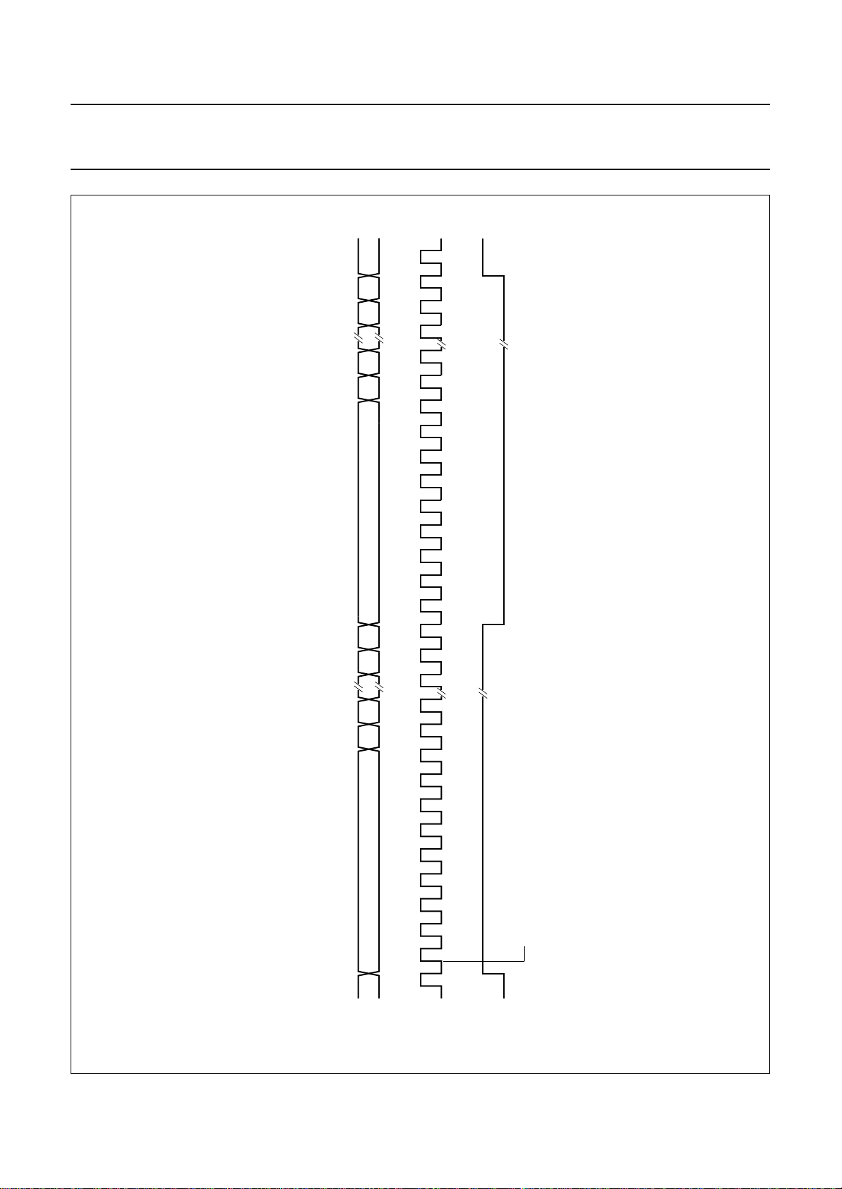
The TDA1545A accepts input serial data formats of 16-bit
word length. Left and right data words are time
multiplexed. The most significant bit (bit 1) must always be
first. The format of data input is shown in Fig.4 and Fig.5.
With a LOW level on the word select input (WS) input data
is placed in the right input register and with a HIGH level
on the WS input data is placed in the left input register.
The data in the input registers is simultaneously latched in
the output registers which control the bit switches.
An internal bias current I
(see IBL and IBR in Fig.1) is
bias
added to the full scale output current IFS in order to
achieve the maximum dynamic range at the outputs of
OP1 and OP2 (see Fig.1). The reference input current
IREF controls with gain AFS the current IFS which is a sink
current and with gain Abias the I
current (note 1). The current I
the IFS and I
because AFS and A
voltage V
will also be proportional to VDD (note 2)
bias
are constant. The reference output
bias
in Fig.1 is2⁄3 VDD. In this way the maximum
REF
which is a source
bias
is proportional to VDD so
REF
dynamic range is achieved over the entire power supply
range. The tolerance of the reference input current in Fig.1
depends on the tolerance of the resistors R3, R4 and R
REF
(note 3).
Notes to the functional description
1. I
2.
3. ∆I
= AFS× I
FS
V
DD1
==
------------V
DD2
=
REF
–
I
---------------------------------------------------------------------------------------------------------
REF
R3 ∆ R3 R4 ∆R4 R
handbook, full pagewidth
I
FS1
---------I
FS2
REF
and I
I
------------- I
bias1
bias2
bias
= A
V
DD
bias
× I
++++ +
S1
C
gs
REF
∆R
REF
out out
V
gs
M1
S2
REF
I
REF
S1
C
gs
(a)
(b)
I
REF
V
I
REF
S2
M1
gs
MCD289 - 1
March 1993 6
Fig.3 Calibration principle; (a) calibration, (b) operation.
Page 7
Philips Semiconductors Preliminary specification
Stereo continuous calibration DAC TDA1545A
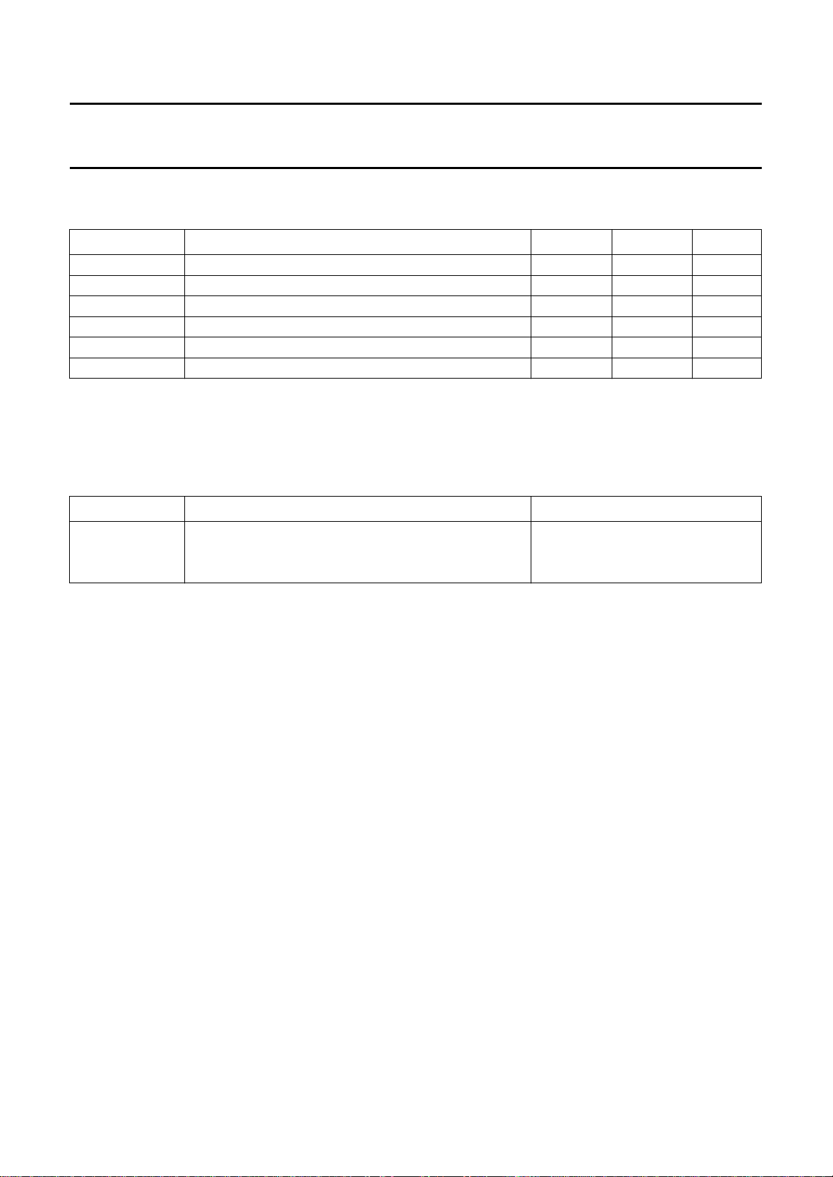
LIMITING VALUES
In accordance with the Absolute Maximum Rating System (IEC 134).
SYMBOL PARAMETER MIN. MAX. UNIT
V
P
T
XTAL
T
stg
T
amb
V
es
V
es
Notes
1. Equivalent to discharging a 100 pF capacitor via a 1.5 kΩ series resistor.
2. Machine model; C = 200 pF, L = 0.5 µH, R = 10 Ω, 3 zaps positive and negative.
THERMAL RESISTANCE
positive supply voltage − 6V
maximum crystal temperature − +150 °C
storage temperature −55 +150 °C
operating ambient temperature −40 +85 °C
electrostatic handling (note 1) −2000 +2000 V
electrostatic handling (note 2) −200 +200 V
SYMBOL PARAMETER THERMAL RESISTANCE
R
th j-a
from junction to ambient in free air
SOT97 100 K/W
SOT96A 210 K/W
March 1993 7
Page 8
Philips Semiconductors Preliminary specification
Stereo continuous calibration DAC TDA1545A
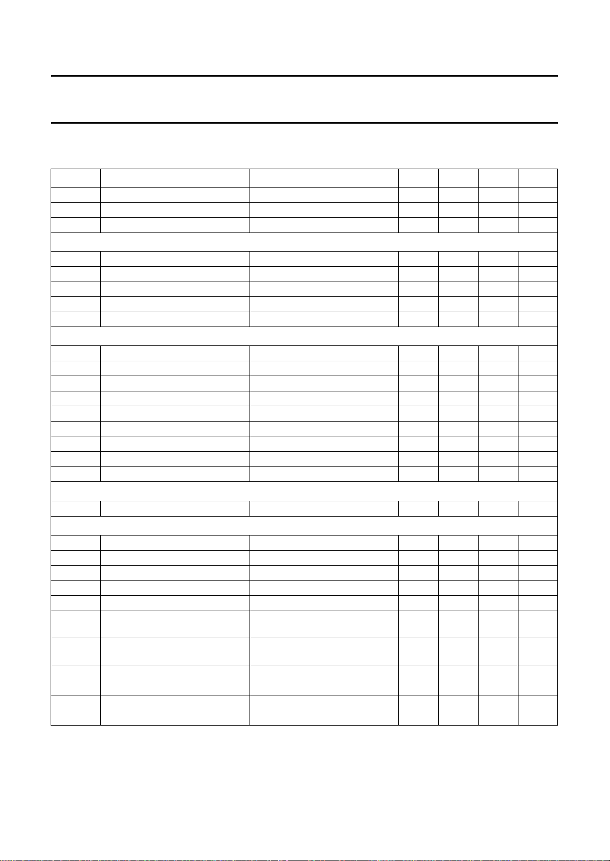
CHARACTERISTICS
= 5 V; T
V
DD
SYMBOL PARAMETER CONDITIONS MIN. TYP. MAX. UNIT
V
DD
I
DD
RR ripple rejection note 2 − 30 − dB
Digital inputs (WS; BCK; DATA)
| input leakage current LOW VI= 0.8 V −−10 µA
|I
IL
| input leakage current HIGH VI= 2.4 V −−10 µA
|I
IH
f
BCK
BR bit rate data input −−18.4 Mbits/s
f
WS
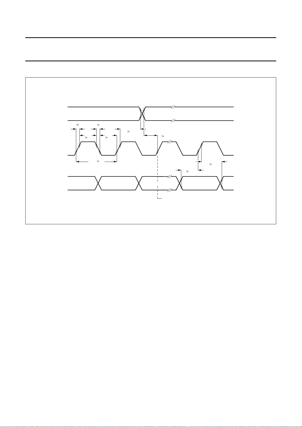
Timing (Fig.4)
t
r
t
f
t
CY
t
HB
t
LB
t
SU;DAT
t
HD;DAT
t
HD;WS
t
SU;WS
Analog input (I
R
REF
Analog outputs (IOL; IOR)
Res resolution −−16 bit
V
DCC
I
FS
T
CFS
I
bias
A
FS
A
bias
THD total harmonic distortion including noise at 0 dB; −−88 −78 dB
THD total harmonic distortion including noise at −60 dB; −−33 −24 dB
= +25 °C; measured in the circuit of Fig.1; unless otherwise specified.
amb
supply voltage 3.0 5.0 5.5 V
supply current note 1 − 3.0 4.0 mA
bit clock input frequency −−18.4 MHz
word select input −−384 kHz
rise time −−12 ns
fall time −−12 ns
bit clock cycle time 54 −−ns
bit clock HIGH time 15 −−ns
bit clock LOW time 15 −−ns
data set-up time 12 −−ns
data hold time 2 −−ns
word select hold time 2 −−ns
word select set-up time 12 −−ns
)
REF
reference resistor (Fig.1) 7.4 11.0 14.6 kΩ
DC output voltage compliance 2.0 − VDD−1V
full scale current 0.9 1.0 1.1 mA
full scale temperature coefficient −±400 − ppm
bias current 643 714 785 µA
reference input current to full
− 13.2 −
scale output current gain
reference input current to bias
− 9.42 −
current gain
note 3, see Fig.6 − 0.004 0.01 %
note 3, Fig.6 − 2.2 6 %
March 1993 8
Page 9
Philips Semiconductors Preliminary specification
Stereo continuous calibration DAC TDA1545A
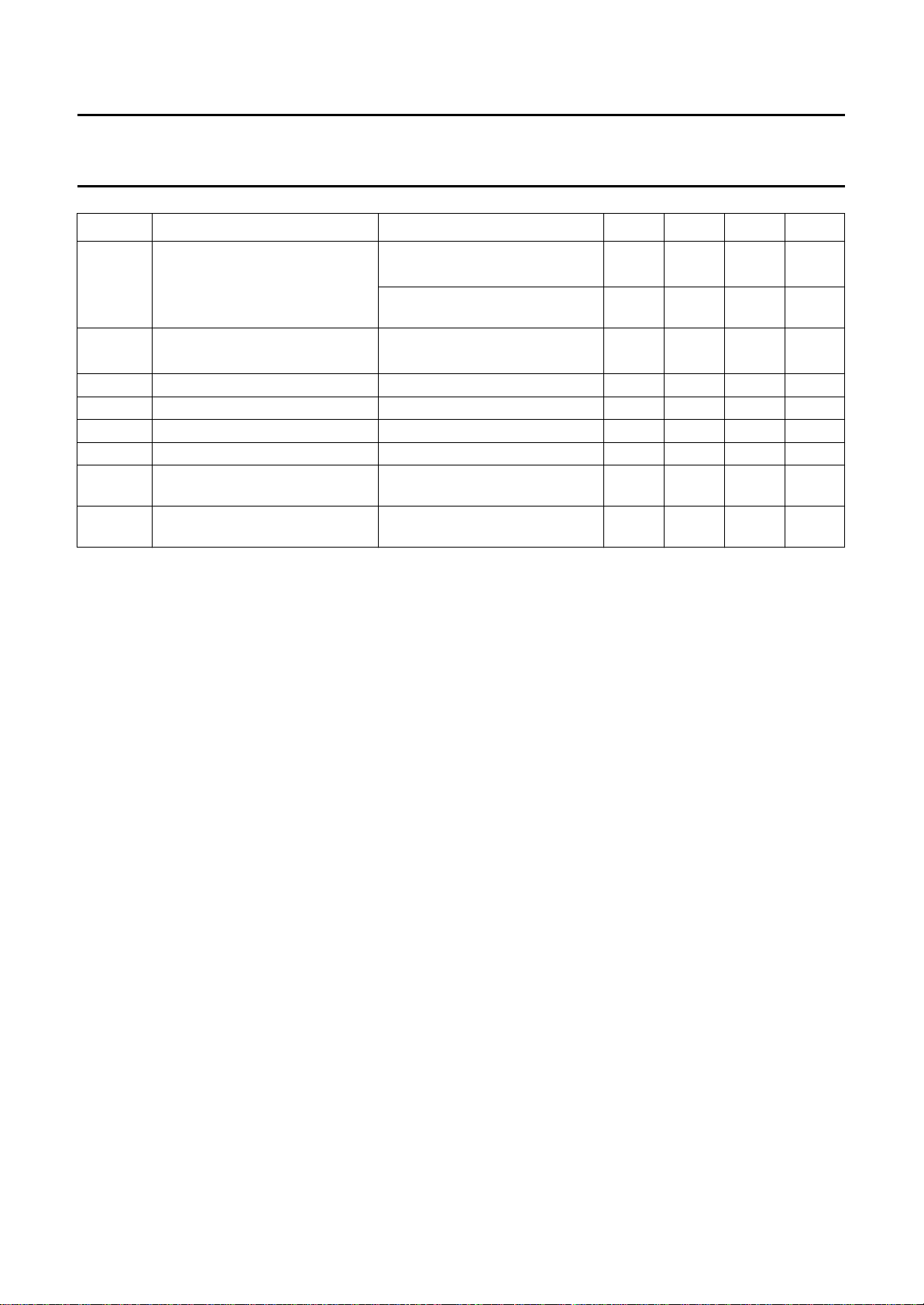
SYMBOL PARAMETER CONDITIONS MIN. TYP. MAX. UNIT
THD total harmonic distortion including noise at −60 dB, −−35 − dB
A-weigthing − 1.8 − %
R3 = R4 = 11 kΩ see Fig.1;
= 2 mA
I
FS
THD total harmonic distortion including noise at 0 dB; note 4 −−84 −70 dB
t
cs
settling time ± 1 LSB − 0.2 −µs
α channel separation 86 95 − dB
| unbalance between outputs note 3 − 0.2 0.3 dB
|d
IO
| delay time between outputs −±0.2 −µs
|t
d
S/N signal-to-noise ratio
at bipolar zero; note 1 86 98 − dB
(A-weighting)
S/N signal-to-noise ratio
at bipolar zero; note 5 − 101 − dB
(A-weighting)
− 1.4 − %
− 0.006 0.03 %
Notes
1. At code 0000H.
2. V
= 1% of supply voltage and f
ripple
= 100 Hz.
ripple
3. Measured with 1 kHz sinewave generated at a sampling rate of 192 kHz.
4. Measured with 1 kHz sinewave over a 20 Hz to 20 kHz bandwidth generated at a sampling rate of 192 kHz.
5. R3 = R4 = 11 kΩ; see Fig.1; IFS = 2 mA.
March 1993 9
Page 10
Philips Semiconductors Preliminary specification
Stereo continuous calibration DAC TDA1545A
TEST AND APPLICATION INFORMATION
LEFT
handbook, full pagewidth
WS
BCK
RIGHT
t
12
t
HB
15
tf12
tCY54
t
HD;WS
t
LB
15
2
t
SU;WS
12
t
HD;DAT
t
SU;DAT
12
2
r
DATA
LSB
MSB
SAMPLE OUT
Fig.4 Timing and input signals.
MLB001
March 1993 10
Page 11
Philips Semiconductors Preliminary specification
Stereo continuous calibration DAC TDA1545A
MLB002
RIGHT
handbook, full pagewidth
MSB
LSB LSB
Fig.5 Format of input signals.
MSBDATA
March 1993 11
BCK
SAMPLE OUT
WS LEFT
Page 12
Philips Semiconductors Preliminary specification
Stereo continuous calibration DAC TDA1545A
APPLICATION INFORMATION
MGA054
full pagewidth
THD
(dB)
20
(1)
30
10
THD
(%)
40
50
60
70
80
90
10 10
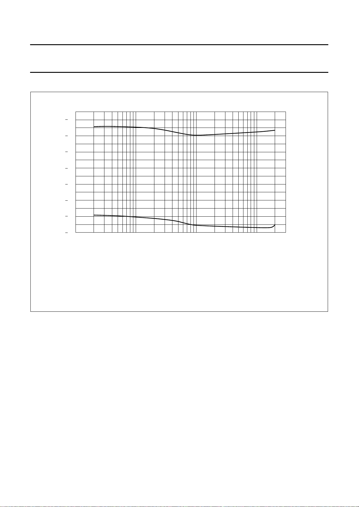
(1) Measured including all distortion plus noise at a level of −60 dB
(2) Measured including all distortion plus noise at a level of −0 dB
The sample frequency 4FS: 176.4 kHz
The graphs are constructed from average values of a small amount of engineering samples therefore no guarantee for typical values
is implied
2
10
(2)
3
frequency (Hz)
4
10
Fig.6 Total harmonic distortion as a function of frequency (4FS).
1
0.1
0.01
March 1993 12
Page 13
Philips Semiconductors Preliminary specification
Stereo continuous calibration DAC TDA1545A
100
handbook, halfpage
THD
(dB)
80
60
40
20
0
100 0
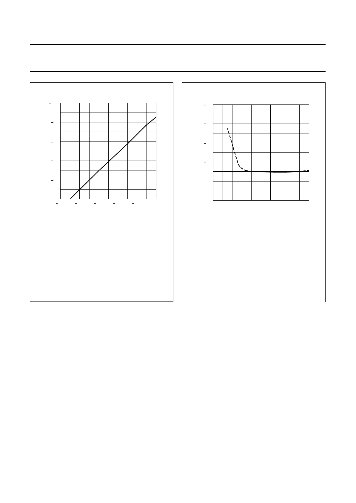
The sample frequency 4FS: 176.4 kHz
The graphs are constructed from average values of a small amount
of engineering samples therefore no guarantee for typical values is
implied
80 60 40 20
signal level (dB)
MGA055
V (V)
DD
MGA056
50
handbook, halfpage
THD
(dB)
60
70
80
90
100
16
(1) Measured within the specified operating supply voltage range
(2) Measured outside the specified operating supply voltage range
The sample frequency 4FS: 176.4 kHz
The graphs are constructed from average values of a small
amount of engineering samples therefore no guarantee for
typical values is implied
(2)
(1)
2345
Fig.7 Total harmonic distortion as a function of
signal level (4FS).
Fig.8 Total harmonic distortion as a function of
supply voltage VDD (4FS).
March 1993 13
Page 14
Philips Semiconductors Preliminary specification
Stereo continuous calibration DAC TDA1545A
PACKAGE OUTLINES
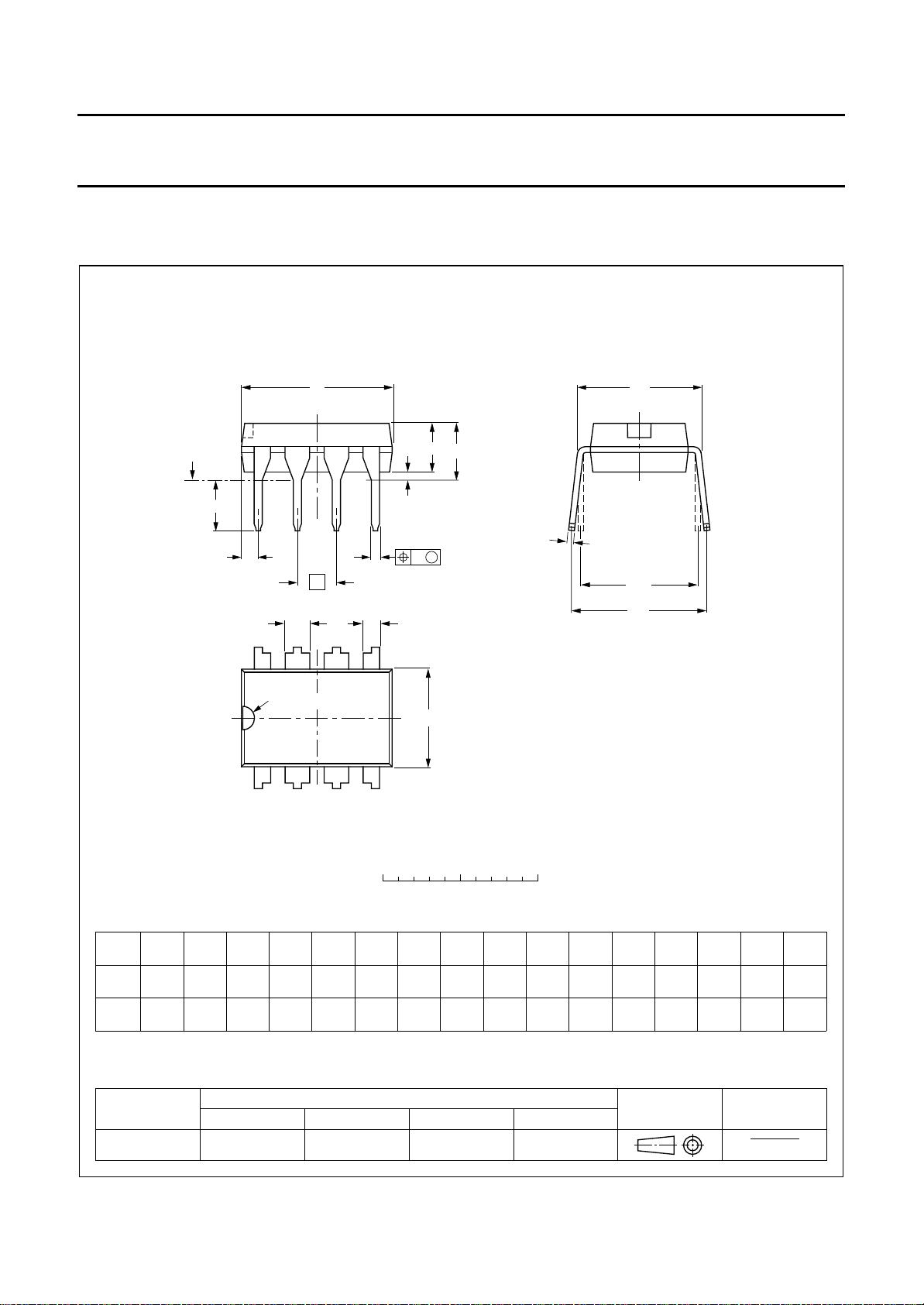
DIP8: plastic dual in-line package; 8 leads (300 mil)
D
seating plane
A
L
Z
e
b
8
pin 1 index
1
w M
b
1
b
2
5
SOT97-1
M
E
A
2
A
c
(e )
1
M
H
E
1
DIMENSIONS (inch dimensions are derived from the original mm dimensions)
A
A
A
UNIT
max.
mm
inches
Note
1. Plastic or metal protrusions of 0.25 mm maximum per side are not included.
OUTLINE
VERSION
SOT97-1
12
min.
max.
050G01 MO-001AN
b
1.73
1.14
0.068
0.045
IEC JEDEC EIAJ
0.53
0.38
0.021
0.015
b
1
1.07
0.89
0.042
0.035
4
0 5 10 mm
scale
b
cD E e M
2
0.36
9.8
0.23
9.2
0.014
0.39
0.009
0.36
REFERENCES
March 1993 14
(1) (1)
6.48
6.20
0.26
0.24
L
3.60
8.25
3.05
7.80
0.14
0.32
0.12
0.31
EUROPEAN
PROJECTION
M
E
10.0
0.39
0.33
e
1
H
8.3
w
max.
0.2542.54 7.62
1.154.2 0.51 3.2
0.010.10 0.30
0.0450.17 0.020 0.13
ISSUE DATE
92-11-17
95-02-04
(1)
Z
Page 15
Philips Semiconductors Preliminary specification
Stereo continuous calibration DAC TDA1545A
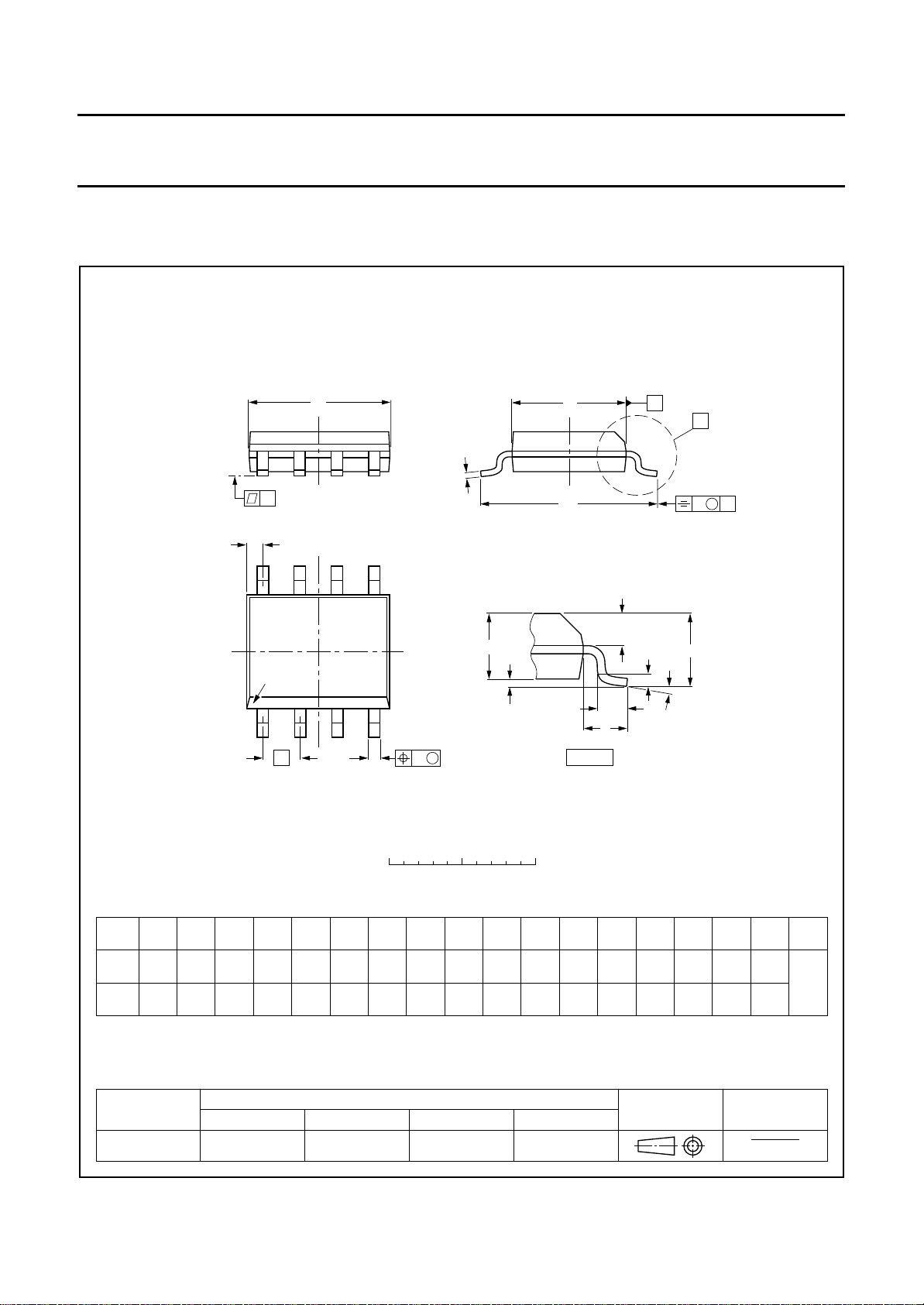
SO8: plastic small outline package; 8 leads; body width 3.9 mm
D
c
y
Z
8
pin 1 index
1
e
5
A
2
A
4
b
w M
p
SOT96-1
E
H
E
1
L
detail X
A
X
v M
A
Q
(A )
L
p
A
3
θ
DIMENSIONS (inch dimensions are derived from the original mm dimensions)
mm
OUTLINE
VERSION
SOT96-1
A
max.
1.75
0.069
A
1
0.25
0.10
0.0098
0.0039
UNIT
inches
Notes
1. Plastic or metal protrusions of 0.15 mm maximum per side are not included.
2. Plastic or metal protrusions of 0.25 mm maximum per side are not included.
March 1993 15
0 2.5 5 mm
A2A
1.45
1.25
0.057
0.049
IEC JEDEC EIAJ
076E03S MS-012AA
0.25
0.01
b
3
p
0.49
0.25
0.36
0.19
0.019
0.0098
0.014
0.0075
(1)E(2)
cD
5.0
4.8
0.20
0.19
REFERENCES
0.16
0.15
scale
eHELLpQZywv θ
4.0
3.8
1.27
0.050
6.2
5.8
0.24
0.23
1.05
1.0
0.4
0.039
0.016
0.7
0.6
0.028
0.024
0.25 0.10.25
0.010.010.041 0.004
EUROPEAN
PROJECTION
(1)
0.7
0.3
0.028
0.012
ISSUE DATE
92-11-17
95-02-04
o
8
o
0
Page 16

Philips Semiconductors Preliminary specification
Stereo continuous calibration DAC TDA1545A
SOLDERING
Introduction
There is no soldering method that is ideal for all IC
packages. Wave soldering is often preferred when
through-hole and surface mounted components are mixed
on one printed-circuit board. However, wave soldering is
not always suitable for surface mounted ICs, or for
printed-circuits with high population densities. In these
situations reflow soldering is often used.
This text gives a very brief insight to a complex technology.
A more in-depth account of soldering ICs can be found in
“IC Package Databook”
our
(order code 9398 652 90011).
DIP
OLDERING BY DIPPING OR BY WAVE
S
The maximum permissible temperature of the solder is
260 °C; solder at this temperature must not be in contact
with the joint for more than 5 seconds. The total contact
time of successive solder waves must not exceed
5 seconds.
The device may be mounted up to the seating plane, but
the temperature of the plastic body must not exceed the
specified maximum storage temperature (T
stg max
). If the
printed-circuit board has been pre-heated, forced cooling
may be necessary immediately after soldering to keep the
temperature within the permissible limit.
R
EPAIRING SOLDERED JOINTS
Apply a low voltage soldering iron (less than 24 V) to the
lead(s) of the package, below the seating plane or not
more than 2 mm above it. If the temperature of the
soldering iron bit is less than 300 °C it may remain in
contact for up to 10 seconds. If the bit temperature is
between 300 and 400 °C, contact may be up to 5 seconds.
to the printed-circuit board by screen printing, stencilling or
pressure-syringe dispensing before package placement.
Several techniques exist for reflowing; for example,
thermal conduction by heated belt. Dwell times vary
between 50 and 300 seconds depending on heating
method. Typical reflow temperatures range from
215 to 250 °C.
Preheating is necessary to dry the paste and evaporate
the binding agent. Preheating duration: 45 minutes at
45 °C.
AVE SOLDERING
W
Wave soldering techniques can be used for all SO
packages if the following conditions are observed:
• A double-wave (a turbulent wave with high upward
pressure followed by a smooth laminar wave) soldering
technique should be used.
• The longitudinal axis of the package footprint must be
parallel to the solder flow.
• The package footprint must incorporate solder thieves at
the downstream end.
During placement and before soldering, the package must
be fixed with a droplet of adhesive. The adhesive can be
applied by screen printing, pin transfer or syringe
dispensing. The package can be soldered after the
adhesive is cured.
Maximum permissible solder temperature is 260 °C, and
maximum duration of package immersion in solder is
10 seconds, if cooled to less than 150 °C within
6 seconds. Typical dwell time is 4 seconds at 250 °C.
A mildly-activated flux will eliminate the need for removal
of corrosive residues in most applications.
EPAIRING SOLDERED JOINTS
R
SO
REFLOW SOLDERING
Reflow soldering techniques are suitable for all SO
packages.
Reflow soldering requires solder paste (a suspension of
fine solder particles, flux and binding agent) to be applied
March 1993 16
Fix the component by first soldering two diagonallyopposite end leads. Use only a low voltage soldering iron
(less than 24 V) applied to the flat part of the lead. Contact
time must be limited to 10 seconds at up to 300 °C. When
using a dedicated tool, all other leads can be soldered in
one operation within 2 to 5 seconds between
270 and 320 °C.
Page 17

Philips Semiconductors Preliminary specification
Stereo continuous calibration DAC TDA1545A
DEFINITIONS
Data sheet status
Objective specification This data sheet contains target or goal specifications for product development.
Preliminary specification This data sheet contains preliminary data; supplementary data may be published later.
Product specification This data sheet contains final product specifications.
Limiting values
Limiting values given are in accordance with the Absolute Maximum Rating System (IEC 134). Stress above one or
more of the limiting values may cause permanent damage to the device. These are stress ratings only and operation
of the device at these or at any other conditions above those given in the Characteristics sections of the specification
is not implied. Exposure to limiting values for extended periods may affect device reliability.
Application information
Where application information is given, it is advisory and does not form part of the specification.
LIFE SUPPORT APPLICATIONS
These products are not designed for use in life support appliances, devices, or systems where malfunction of these
products can reasonably be expected to result in personal injury. Philips customers using or selling these products for
use in such applications do so at their own risk and agree to fully indemnify Philips for any damages resulting from such
improper use or sale.
March 1993 17
 Loading...