

Page 1
TOSHIBA BIPOLAR DIGITAL INTEGRATED CIRCUIT SILICON MONOLITHIC
TD62783AP,TD62783F,TD62783AF
TD62784AP,TD62784F,TD62784AF
8CH HIGH−VOLTAGE SOURCE DRIVER
The TD62783AP / F / AF Series are comprised of eight source
current Transistor Array.
These drivers are specifically designed for fluorescent display
applications.
Applications include relay, hammer and lamp drivers.
FEATURES
l High output voltage Type−AP, AF : VCC = 50 V MIN.
Type−F : VCC = 35 V MIN.
l Output current (single output) I
l Output clamp diodes
l Single supply voltage
l Input compatible with various types of logic
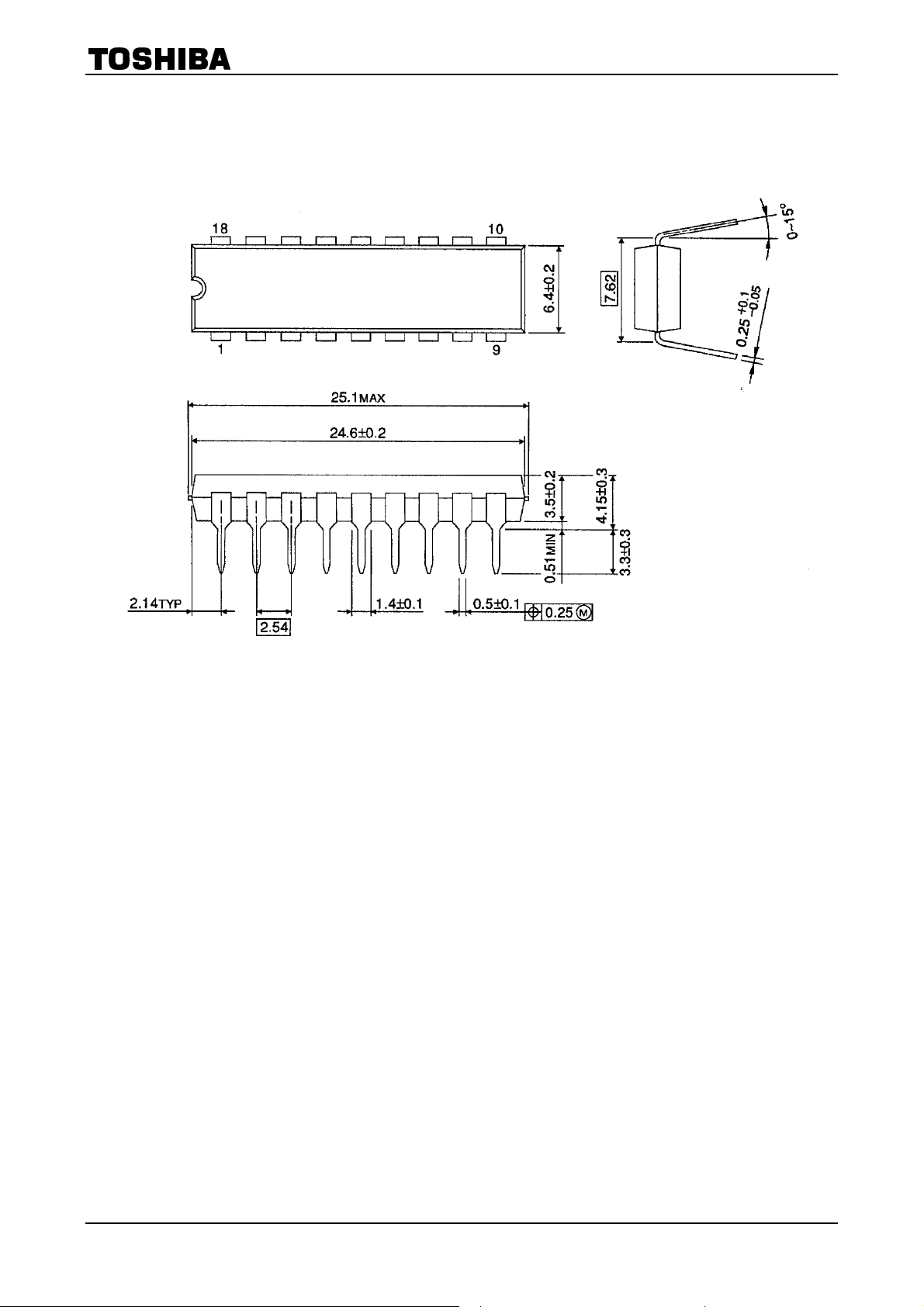
l Package Type−AP : DIP−18 pin
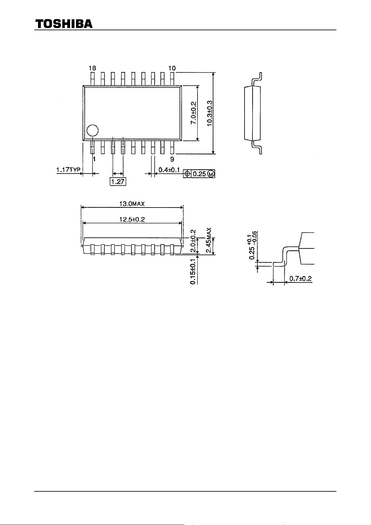
l Package Type−F, AF : SOP−18 pin
= −500 mA MIN.
OUT
TD62783,784AP/F/AF
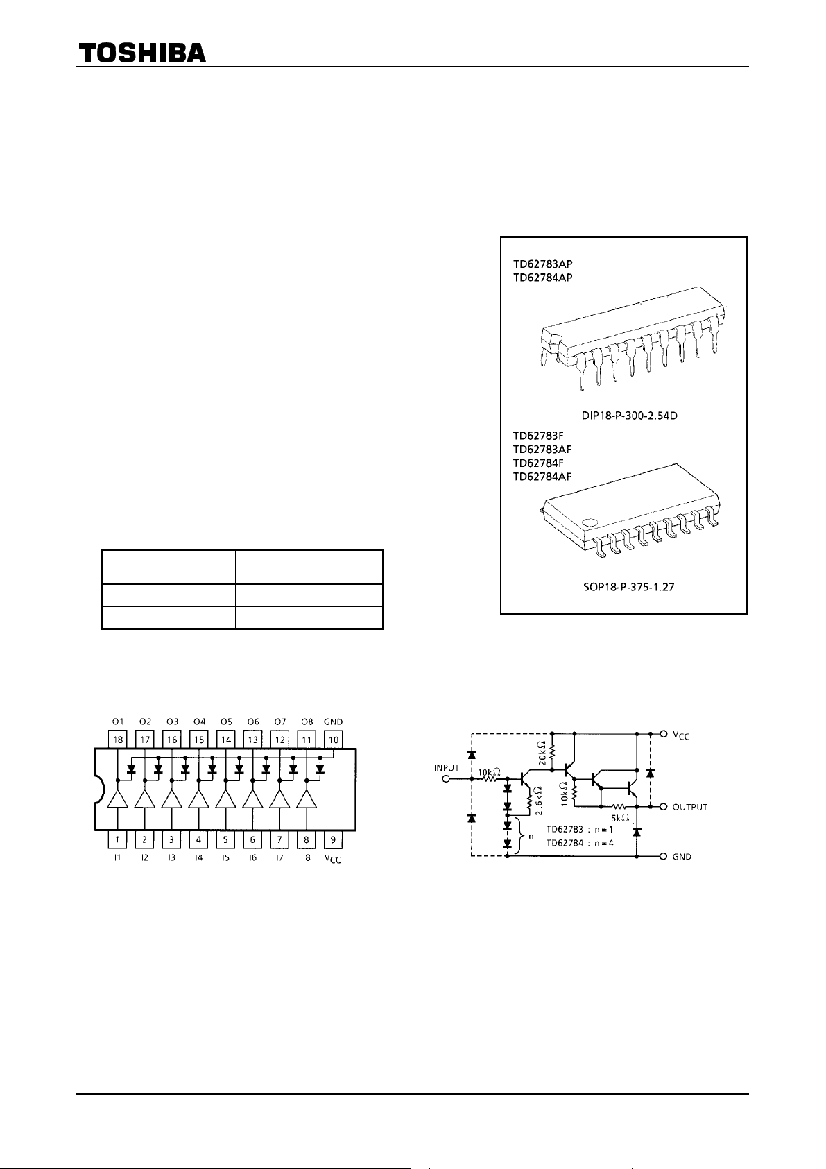
TYPE DESIGNATION
TD62783AP / F / AF TTL, 5 V CMOS
TD62784AP / F / AF 6~15 V PMOS, CMOS
PIN CONNECTION
(TOP VIEW)
Weight
DIP18−P−300−2.54D : 1.47 g (Typ.)
SOP18−P−375−1.27 : 0.41 g (Typ.)
SCHEMATICS
Note: The input and output parasitic diodes cannot
be used as clamp diodes.
(EACH DRIVER)
1
2001-07-05
Page 2
TD62783,784AP/F/AF
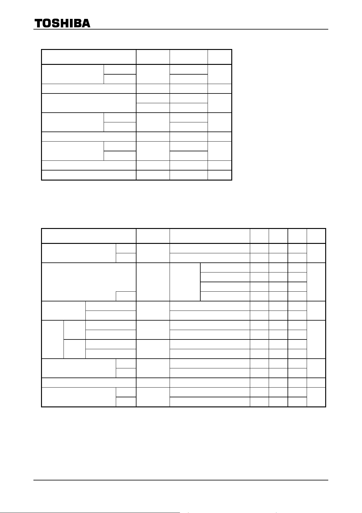
MAXIMUM RATINGS
CHARACTERISTIC SYMBOL RATING UNIT
Supply Voltage
Output Current I
Input Voltage
Clamp Diode Reverse
Voltage
Clamp Diode Forward Current I
Power Dissipation
Operating Temperature T
Storage Temperature T
(Ta = 25°C)
AP, AF 50
F
AP, AF 50
F
AP 1.47
F, AF
V
CC
OUT
VIN (Note 1) 15
(Note 2) 30
V
IN
V
R
F
PD (Note 3)
opr
stg
35
−500 mA / ch
35
500 mA
0.96
−40~85 °C
−55~150 °C
V
V
V
W
Note 1: Only TD62783AP / F / AF
Note 2: Only TD62784AP / F / AF
Note 3: Delated above 25°C in the proportion of 11.7 W / °C (AP Type), 7.7 W / °C (F, AF Type)
RECOMMENDED OPERATING CONDITIONS
(Ta = −40~85°C)
CHARACTERISTIC SYMBOL TEST CONDITION MIN TYP. MAX UNIT
Supply Voltage
Output Current
AF, F
Input Voltage
Output
Input
Voltage
Clamp Diode Reverse
Voltage
Clamp Diode Forward Current I
Power Dissipation
On
Output
Off
TD62783AP / F / AF ― ― ― 12
TD62784AP / F / AF
TD62783AP / F / AF ― 2.0 5.0 15
TD62784AP / F / AF
TD62783AP / F / AF ― 0 ― 0.8
TD62784AP / F / AF
AP, AF ― ― ― 50
F
AP ― ― ― 50
F, AF
AP ― ― ― 0.52
F, AF
V
I
OUT
V
V
IN (ON)
V
IN (OFF)
V
P
CC
IN
R
F
D
Ta = 85°C
Tj = 120°C
T
= 25ms
pw
― ― ― 35
Duty = 10% 8Circuits ― ― −260
Duty = 50% 8Circuits ― ― −59
Duty = 10% 8Circuits ― ― −180
Duty = 50% 8Circuits ― ― −38
― ― ― 24
― 4.5 12.0 30
― 0 ― 2.0
― ― ― 35
―
― ― ― 0.35
― ― 400 mA
V
mA /
ch
V
V
V
W
2
2001-07-05
Page 3
TD62783,784AP/F/AF
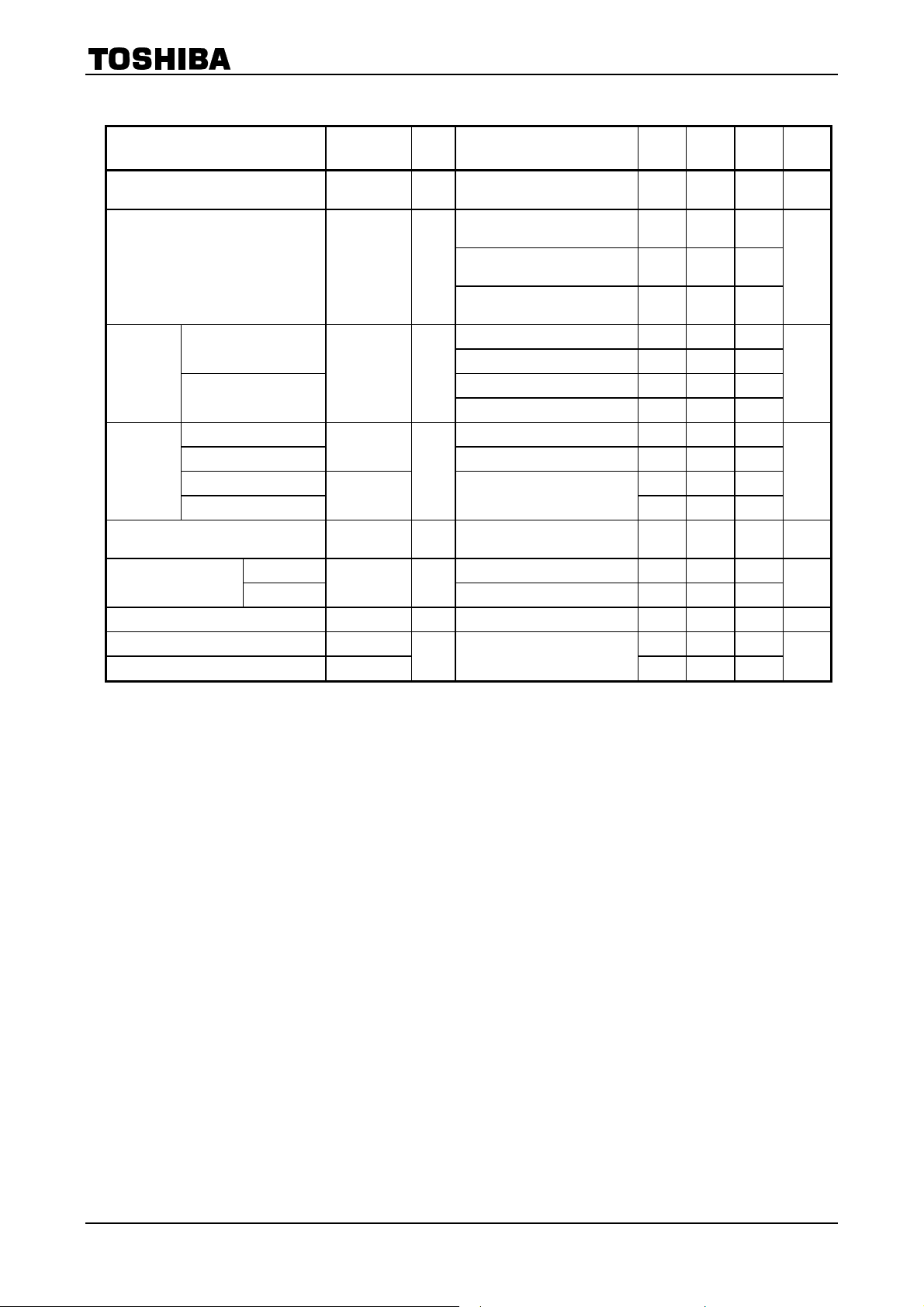
ELECTRICAL CHARACTERISTICS
CHARACTERISTIC SYMBOL
Output Leakage Current I
Output Saturation Voltage V
TD62783AP / F / AF
Input
Current
TD62784AP / F / AF
TD62783AP / F / AF VCE = 2.0 V ― ― 2.0
Input
Voltage
TD62784AP / F / AF
TD62783AP / F / AF 0.8 ― ―
TD62784AP / F / AF
Supply Current I
Clamp Diode
Reverse Current
AP, AF VR = 50 V ― ― 50
F
Clamp Diode Forward Voltage V
Turn−On Delay t
Turn−Off Delay t
CEX
CE (sat)
I
IN (ON)
V
IN (ON)
V
IN (OFF)
CC (ON)
I
R
F
ON
OFF
(Ta = 25°C)
TEST
CIR−
TEST CONDITION MIN TYP. MAX UNIT
CUIT
1
2
= V
V
CC
= −350 mA
OUT
= −225 mA
OUT
= V
IN
= −100 mA
OUT
CC MAX. VIN
IN (ON)
IN (ON)
IN (ON)
Ta = 25°C
VIN = V
I
VIN = V
I
V
I
= 0.4 V
,
,
,
― ― 100 µA
― ― 2.0
― ― 1.9
― ― 1.8
VIN = 2.4 V ― 36 52
= 3.85 V ― 180 260
V
IN
3
VIN = 5 V ― 92 130
= 12 V ― 790 1130
V
IN
I
= −350 mA ― ― 4.5
OUT
4
I
= −500 µA
OUT
3 VIN = V
2.0 ― ―
, VCC = 50 V ― ― 2.5
IN (ON)
5
= 35 V ― ― 50
V
R
6 IF = 350 mA ― ― 2.0 V
= VCC
V
CC
7
C
= 15 pF, RL = 88 Ω (F)
L
MAX. RL
= 125 Ω
― 0.15 ―
― 1.8 ―
V
µA
V
mA /
ch
µA
µs
3
2001-07-05
Page 4
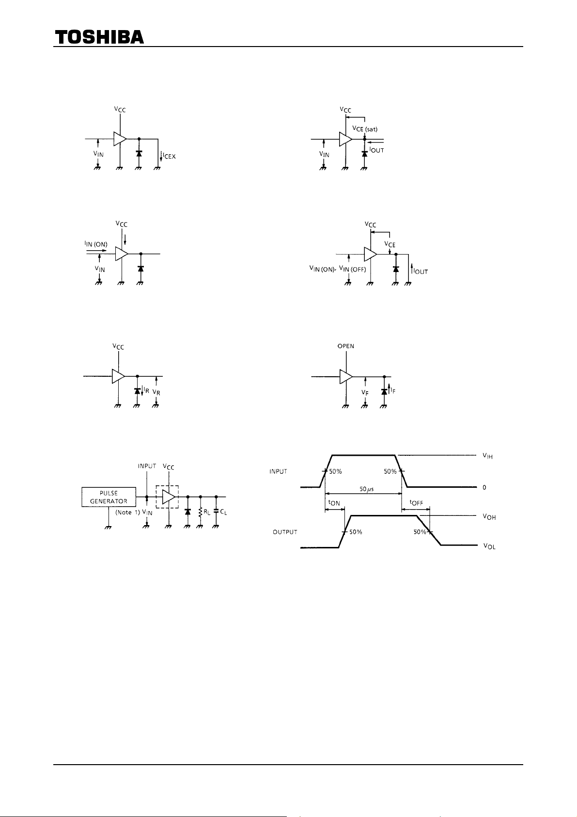
TEST CIRCUIT
TD62783,784AP/F/AF
1. I
3. I
5. I
CEX
IN (ON)
R
, I
CC
2. V
CE (sat)
4. V
IN (ON)
, V
IN (OFF)
6. VF
7. tON, t
Note 1: Pulse width 50 µs, duty cycle 10%
Output impedance 50 Ω, t
Note 2: C
OFF
≤ 5 ns, tf ≤ 10 ns
r
includes probe and jig capacitance
L
PRECAUTIONS for USING
This IC does not integrate protection circuits such as overcurrent and overvoltage protectors.
Thus, if excess current or voltage is applied to the IC, the IC may be damaged. Please design the IC so that
excess current or voltage will not be applied to the IC.
Utmost care is necessary in the design of the output line, V
short−circuit between outputs, air contamination fault, or fault by improper grounding.
and GND line since IC may be destroyed due to
CC
4
2001-07-05
Page 5
TD62783,784AP/F/AF
5
2001-07-05
Page 6
TD62783,784AP/F/AF
6
2001-07-05
Page 7
TD62783,784AP/F/AF
PACKAGE DIMENSIONS
DIP18−P−300−2.54D Unit: mm
Weight: 1.47 g (Typ.)
7
2001-07-05
Page 8
TD62783,784AP/F/AF
PACKAGE DIMENSIONS
SOP18−P−375−1.27 Unit: mm
Weight: 0.41 g (Typ.)
8
2001-07-05
Page 9
TD62783,784AP/F/AF
A
RESTRICTIONS ON PRODUCT USE
· TOSHIBA is continually working to improve the quality and reliability of its products. Nevertheless, semiconductor
devices in general can malfunction or fail due to their inherent electrical sensitivity and vulnerability to physical
stress. It is the responsibility of the buyer, when utilizing TOSHIBA products, to comply with the standards of
safety in making a safe design for the entire system, and to avoid situations in which a malfunction or failure of
such TOSHIBA products could cause loss of human life, bodily injury or damage to property.
In developing your designs, please ensure that TOSHIBA products are used within specified operating ranges as
set forth in the most recent TOSHIBA products specifications. Also, please keep in mind the precautions and
conditions set forth in the “Handling Guide for Semiconductor Devices,” or “TOSHIBA Semiconductor Reliability
Handbook” etc..
· The TOSHIBA products listed in this document are intended for usage in general electronics applications
(computer, personal equipment, office equipment, measuring equipment, industrial robotics, domestic appliances,
etc.). These TOSHIBA products are neither intended nor warranted for usage in equipment that requires
extraordinarily high quality and/or reliability or a malfunction or failure of which may cause loss of human life or
bodily injury (“Unintended Usage”). Unintended Usage include atomic energy control instruments, airplane or
spaceship instruments, transportation instruments, traffic signal instruments, combustion control instruments,
medical instruments, all types of safety devices, etc.. Unintended Usage of TOSHIBA products listed in this
document shall be made at the customer’s own risk.
· The products described in this document are subject to the foreign exchange and foreign trade laws.
· The information contained herein is presented only as a guide for the applications of our products. No
responsibility is assumed by TOSHIBA CORPORATION for any infringements of intellectual property or other
rights of the third parties which may result from its use. No license is granted by implication or otherwise under
any intellectual property or other rights of TOSHIBA CORPORATION or others.
000707EB
· The information contained herein is subject to change without notice.
9
2001-07-05
Page 10

This datasheet has been download from:
www.datasheetcatalog.com
Datasheets for electronics components.
 Loading...