

Page 1
TD350
Advanced IGBT/MOSFET Driver
■ 0.75A source/1.2A sink min gate drive
■ Active Miller clamp feature
■ Two steps turn-off with adjustable level
and delay
■ Desaturation detection
■ Fault status output
■ Negative gate drive ability
■ Input compatible with pulse transformer or
optocoupler
■ Separate sink and source outputs for easy
gate dr i ve
■ UVLO protection
■ 2kV ESD protection
Description
TD350 is an advanced gate driver for IGBT and
power MOSFET. Control and protection functions
are included and allow the design of high reliability
systems.
Innovative active Miller clamp function avoids the
need of negative gate drive in most applications
and allows th e use of a simple bo otstrap supply
for the high side driver
TD350 includes a two-level turn-off feature with
adjustable level and delay. This function protects
against excessive overvoltag e at turn-off in case
of overcurrent or short-circuit condition. Same
delay is applied at turn-on to prevent pulse width
distortion.
TD350 also includes an IGBT desaturation
protection and a FAULT status output.
TD350 is compat ible with both pulse transformer
and optocoupler signals.
Applications
■ 1200V 3-Phase Inverter
■ Motor C
ontrol
■ UPS Systems
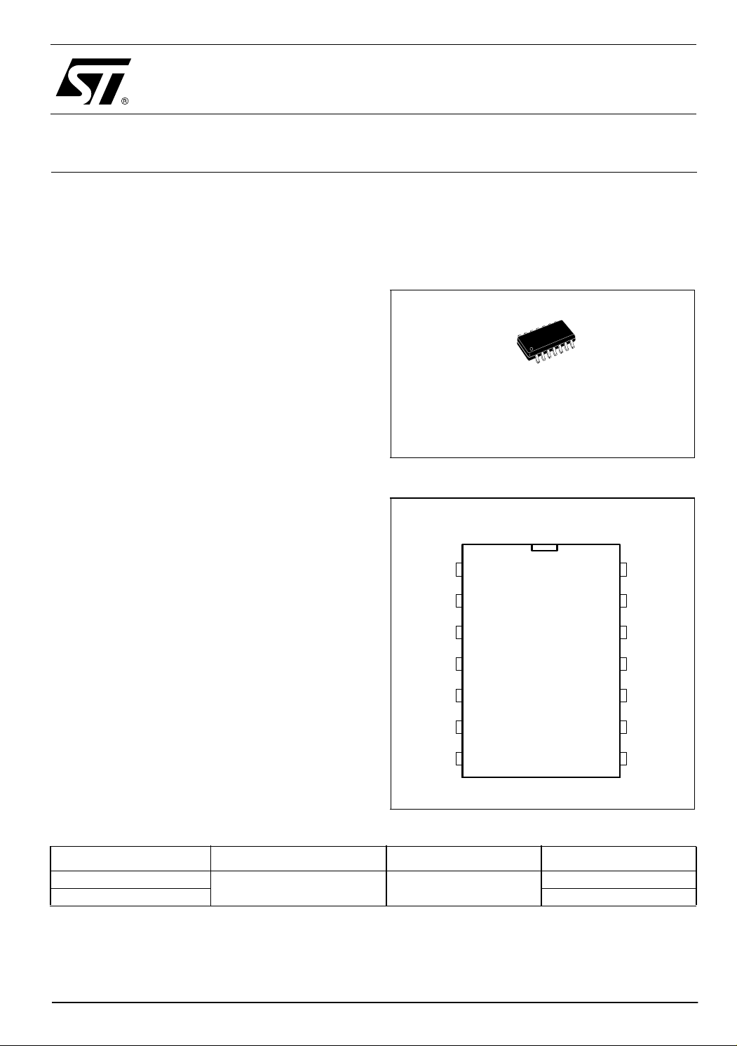
D
SO-14
(Plastic MicroPacka ge)
Pin Connections (top view )
1
IN
VREF
FAULT
NC
COFF
NC
LVOFF
2
3
4
5
6
7
TD350
14
11
13
12
10
DESAT
VH
OUTH
OUTL
VL
9
CLAMP
8
GND
Order Codes
Part Number Temperature Range Package Packaging
TD350ID
TD350IDT Tape & Reel
August 2004 Revision 1 1/11
-40, +125°C SO
Tube
Page 2
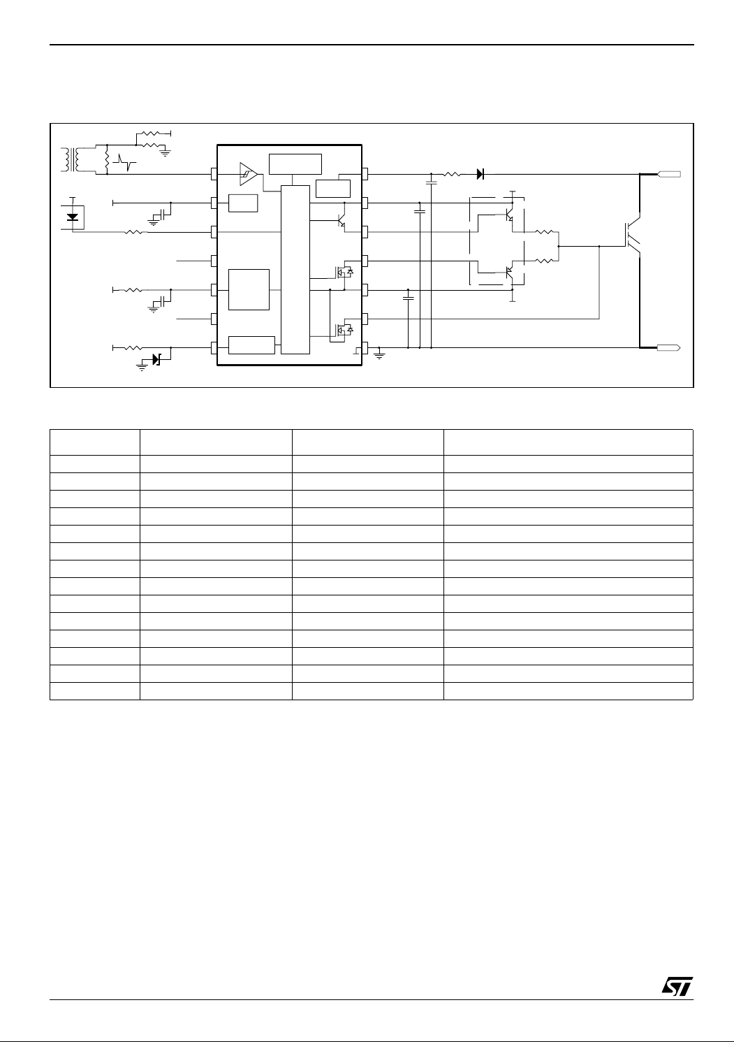
TD350 Block Diagram
1 Block Diagram
Figure 1: Sche m atic block diagram
Vref
Off
UVLO
DESAT
Desat
Control Block
VH
OUTH
OUTL
VL
CLAMP
GND
16V
Optionnal
-10V
Pulse Transformer
VH
Vref
Vref
VH
IN
VREF
FAULT
NC
COFF
NC
LVOFF
Vref
delay
Off Level
TD350
Table 1: Pin description
Name Pin Number Type Function
IN 1 Analog input Input
VREF 2 Analog output +5V reference voltage
FAULT 3 Digital output Fault status output
NC 4 Not connected
COFF 5 Timing capacitor Turn off delay
NC 6 Not connected
LVOFF 7 Analog input Turn off level
GND 8 Power supply Signal ground
CLAMP 9 Analog output Miller clamp
VL 10 Power supply Negative supply
OUTL 11 Analog output Gate drive output (sink)
OUTH 12 Analog output Gate drive output (source)
VH 13 Power supply Positive supply
DESAT 14 Analog input Desaturation protection
2/11
Page 3
Absolute Maximum Ratin gs TD350
2 Absolute Maximum Rat ings
Table 2: Key parameters and their absolute maximum ratings
Symbol Parameter Value Unit
VHL Maximum Supply Voltage (VH - VL) 28 V
VH Maximum VH voltage vs. GND 28 V
VL Minimum VL voltage vs. GND -12 V
Vout Voltage on OUTH, OUTL, CLAMP pins VL-0.3 to VH+0.3 V
Vdes Voltage on DESAT, FAULT, LVOFF pin -0.3 to VH+0.3 V
Vter Voltage on other pins (IN, COFF, VREF) -0.3 to 7 V
Pd Power dissipation 500 mW
Tstg Storage temperature -55 to 150 °C
Tj Maximum Junction Temperature 150 °C
Rhja Thermal Resis tance Junction-A mbie nt 125 °C/W
Rhjc The rmal Resis tance Junction-C ase 22 °C/W
ESD Electrostatic discharge 2 kV
Table 3: Operat in g conditions
Symbol Parameter Value Unit
VH Positive Supply Voltage vs. GND UVLO to 26 V
VL Negative Supply Voltage vs. GND 0 to -10 V
VH-VL Maximum Total Supply Voltage 26 V
Toper Operating Free Air Temperature Range -40 to 125 °C
3/11
Page 4

TD350 Electrical Characteristics
3 Electrical Characteristics
Table 4: T
Symbol Parameter Test Condi t io n Min Ty p Max Unit
Input
Vton IN turn-on threshold voltage 0.8 1.0 V
Vtoff IN turn-off threshold voltage 4.0 4.2 V
tonmin Minimum pulse width 100 135 220 ns
Iinp IN Input current 1
Voltage reference - note
Vref Voltage reference
Iref Maximum output current 10 mA
Desaturation protection
Vdes Desaturation threshold 6.5 7.2 7.9 V
Ides Source current 250
Fault output
tfault Delay for fault detection 500 ns
VFL FAULT low voltage Ifsink=10mA 1 V
Clamp
Vtclamp CLAMP pin voltage threshold 2.0 V
VCL Clamp low voltage at Icsink=500mA
Off Delay
Vtdel Voltage threshold 2.35 2.50 2.65 V
Rdel Disch arge resisto r I=1mA 500
Off Levels
Iblvoff LVOFF peak input current (sink) LVOFF=12V 120 200
Violv Offset voltage LVOFF=12V -0.3 -0.15 0 V
Outputs
VOL1 Output low voltage at Iosink=20mA VL+0.35 V
VOL2 Output low voltage at Iosink=200mA
VOL3 Output low voltage at Iosink=500mA
VOH1 Output high voltage 1 Iosource=20mA VH-2.5 V
VOH2 Output high voltage 2 Iosource=200mA VH-3.0 V
VOH3 Output high voltage 3 Iosource=500mA VH-4.0 V
tr Rise time
tf
tpd
∆tw Input to output pulse distortion 10% output change 10 60 110 ns
Under Voltage Lockout (UVLO)
UVLOH UVLO top threshold 10 11 12 V
UVLOL UVLO bottom threshold 9 10 11 V
Vhyst UVLO hysteresis UVH-UVL 0.5 1 V
Supply current
Iin Quiescent current output=0V, no load 5 mA
1) Recommended capac itor range on VR E F pi n i s 10nF to 100nF.
4/11
= -20 to 125°C, VH=16V, VL=-10V (unless otherwise spe cified)
amb
1
T=25°C
Tmin<T<Tmax
T=25°C
Tmin<T<Tmax
T=25°C
Tmin<T<Tmax
T=25°C
Tmin<T<Tmax
CL=1nF, 10% to 90%
VL=0
VL=-10V
Fall time
(2 step turn-off disabled)
Input to output propagation delay at
turn-on (2 step delay disabled)
CL=1nF, 90% to 10%
VL=0
VL=-10V
10% output change
4.85
4.77
270 800 ns
5.00 5.15
5.22
VL+2.5
VL+3.0
VL+1.0
VL+1.5
VL+2.5
VL+3.0
130
175
75
90
µA
V
V
µA
V
V
Ω
µA
V
V
V
V
ns
ns
ns
ns
Page 5

Functional Description TD350
4 Functional Description
4.1 Input
The input is compatible with optocouplers or pulse
transformers. The input is triggered by the signal
edge and allows the use of low-sized, low-cost
pulse transformer. Input is active low (output is
high when input is low) to ease the use of
optocoupler. When driven by a pulse transformer,
the input pulse (positive and negative) width must
be larger than the minimum pule width t
onmin
.
4.2 Voltage reference
A voltage reference is used to create accurate
timing for the two-level turn-off with external
resistor and capacitor.
4.3 Desaturation protection
Desaturation protection e nsures the protection of
the IGBT in the event of overcurrent. When the
DESAT voltage goes higher that 7V, the output is
driven low (w ith 2 -le vel t urn- off if a pp licable ). T he
FAULT output is activated. The FAULT state is
exited at the next falling edge of IN input.
A programmable blanking time is used to allow
enough time for IGBT saturation. Blanking time is
provided by an internal current source and
external capacitor.
DESAT input can also be used with an external
comparator for overcurrent or over temperature
detection.
4.4 Active Miller clamp
A Miller clamp allows the control of the Miller
current during a high dV/dt situation and can avoid
the use of a negative supply voltage.
During turn-off, the gate voltage is monitored a nd
the clamp output is activated when g ate voltage
goes below 2V (relative to GND). The clamp
voltage is VL+3V max for a Miller current up to
500mA. The cla mp is disabled w hen the IN input
is triggered again.
4.5 Two level turn-off
The two-level turn-off is used to increase the
reliability of the application.
During turn-off, gate voltage can be reduc ed to a
programmable leve l in order to reduce the IGBT
current (in the event of over-current). This action
avoids both dangerous overvoltage across the
IGBT, and RBSOA problems, especially at short
circuit turn-off.
Turn-off (T
) delay is programmable through an
a
external resistor and capacitor for accurate timing.
Turn-off delay (T
) is also used to delay t he input
a
signal to prevent distortion of input pulse width.
4.6 Minimum ON t ime
In order to ensure the proper operation of the 2level turn-off function, the input ON time (T
must be greater than the T
T
winmin=Ta
R
is the internal discharge resistor and C
del
+2*R
del*Coff
winmin
value:
off
win
is
the external timing capacitor.
Input signals smaller than Ta are ignored. Input
signals larger than T
output stage after the T
width distortion (
∆T
w=Twout-Twin
For an input signal width T
T
T
, the output width T
winmin
(pulse distortion) and the IGBT could be
win
are transmitted to the
winmin
delay with minimum
a
).
between Ta and
win
is reduced below
wout
partially turned on. These input signa ls should be
avoided during normal operation.
4.7 Output
The output stage is able to sink 2.3A and source
1.5A typical at 25°C (1.2A/0.75A minimum over
the full temperature range). Separated sink and
source outputs allow independent gate charge
and discharge control without an extra external
diode.
)
5/11
Page 6

TD350 Functional Description
4.8 Fault status output
Fault output is used to signal a fault event
(desaturation, UVLO) to a controller. The fault pin
is designed to drive an optocoupler.
4.9 Undervoltage protection
Undervoltage detection protects t he application in
the event of a low VH supply voltage (during startup or a fault situation). During undervoltage, the
OUTH pin is open and the OUTL pin is driven l ow
(active pull-down for VH>2V, passive pull-down
Figure 2: Detailed Internal Schematic
IN
Comp_Input
Delay
1V-4V
for VH<2V). Fault output s ignals the und ervo ltage
state and is reset only when undervoltage state
disappears.
VH
OUT
FAULT
UVLO
UVH
Vref
VH
250uA
VREF
UVL
Vccmin
2V
COFF
LVOFF
Comp_Desat
7.2V
DESAT
Control Block
Vref
Comp_DelayOff
2.5V
S2
VH
Comp_Clamp
2V
2-level OF F driver
FAULT
CLAMP
VH
OUTH
OUTL
VL
GND
6/11
rev. 3
Page 7

Timing Diagrams TD350
5 Timing Diagrams
Figure 3: Turn-on and turn-off
IN
COFF
Ta
OUT
CLAMP
Vge
Vce
VL level
Figure 4: Minim um ON time
Tin<Ta Tin>Twinmin
IN
2.5V
COFF
Ta<Tin<Twinmin
Twin
Ta
VH level
Twout
Open
VH level
Miller plateau
Ta
Ta Ta
VH level
LVOFF
VL level
Clamp threshold
LVOFF
OUT
CLAMP
Figure 5: Desaturation fault
IN
COFF
OUT
DESAT
FAULT
Ta
Open
2.5V
Ta
Desat Blanking Time
VL level
Ta
VH level
LVOFF
VL level
7V
open
7/11
Page 8

TD350 Typical Performance Curves
6 Typical Performance Curves
Figure 6: Supply current vs temperature
5.0
4.0
3.0
In (mA)
2.0
1.0
0.0
-50-250 255075100125
Temp (°C)
Figu re 7: Lo w le vel output v oltag e v s te mp.
3.0
3.0
2.0
2.0
Iosink=500mA
Iosink=500mA
VOL-VL (V)
VOL-VL (V)
1.0
1.0
Iosink=200mA
Iosink=200mA
Figure 9: Voltage reference vs temper ature
5.20
5.10
5.00
Vref (V)
4.90
4.80
-50 -25 0 25 50 75 100 125
Temp (°C)
Figure 10: High level output voltage vs temp.
4.0
4.0
3.0
3.0
Iosource=500mA
Iosource=500mA
2.0
2.0
VH-VOH ( V)
VH-VOH ( V)
1.0
1.0
Iosource=200mA
Iosource=200mA
Iosource=20mA
Iosource=20mA
Iosink=20mA
0.0
0.0
-50 -25 0 25 50 75 100 125
-50 -25 0 25 50 75 100 125
Temp (°C)
Temp (°C)
Iosink=20mA
Figure 8: Desaturation threshold vs
temperature
10
9
8
Vdes (V)
7
6
5
-50 -25 0 25 50 75 100 125
Temp (°C)
8/11
0.0
0.0
-50 -25 0 25 50 75 100 125
-50 -25 0 25 50 75 100 125
Temp (°C)
Temp (°C)
Figure 11: Desaturation source current vs
temp.
500
400
300
200
Ides (uA)
100
0
-50 -25 0 25 50 75 100 125
Temp (°C)
Page 9

Application Diagrams TD350 7 Application Diagrams
Figure 12: Single supply IGBT drive with active Miller clamp and 2-level turn-off
VH
Vref
VH
5.1V
Vref
IN
VREF
FAULT
NC
COFF
NC
LVOFF
Vref
Off Level
Off
delay
UVLO
DESAT
Desat
Control Block
VH
OUTH
OUTL
VL
CLAMP
GND
16V
TD350
Figure 13: Large IGBT drive with negative gate drive and desaturation detection
Vref
Off
delay
UVLO
DESAT
Desat
Control Block
VH
OUTH
OUTL
VL
CLAMP
16V
-10V
Pulse Transform er
VH
Vref
Vref
IN
VREF
FAULT
NC
COFF
NC
Vref
VH
LVOFF
Off Level
GND
TD350
Figure 14: Use of DESAT input for direct overcurrent detection
Vref
Off
delay
UVLO
TD350
DESAT
Desat
Control Block
VH
OUTH
OUTL
VL
CLAMP
GND
16V
Pulse Transform er
VH
Vref
VH
Vref
IN
VREF
FAULT
NC
COFF
NC
LVOFF
Vref
Off Level
Vref
9/11
Page 10

TD350 PACKAGE MECHANICAL DATA
8 PACKAGE MECHANICAL DATA
SO-14 MECHANICAL DATA
DIM.
A 1.75 0.068
a1 0.1 0.2 0.003 0.007
a2 1.65 0.064
b 0.35 0.46 0.013 0.018
b1 0.19 0.25 0.007 0.010
C 0.5 0.019
c1 45˚ (typ.)
D 8.55 8.75 0.336 0.344
E 5.8 6.2 0.228 0.244
e 1.27 0.050
e3 7.62 0.300
F 3.8 4.0 0.149 0.157
G 4.6 5.3 0.181 0.208
L 0.5 1.27 0.019 0.050
M 0.68 0.026
S˚ (max.)
MIN. TYP MAX. MIN. TYP. MAX.
mm. inch
8
10/11
PO13G
Page 11

Revision History TD350
9 Revision History
Date Revision Description of Changes
01 August 2004 1 First Release
Information furnished is believed to be accurate and reliable. However, STMicroelectronics assumes no responsibility for the consequences
of use of such information nor for any infringement of patents or other rights of third parties which may result from its use. No li cens e is g r ante d
by impl i cation or otherwise under any p atent or patent rights of STMicroelectroni cs. Specif i cations mentioned in this publi cation are subject
to change without notice. This publication supersedes and replaces all information previously supplied. STMicroelectronics produc ts are not
authori zed for use as cr i tical components in life support devices or systems without express written approval of S T M i croelectronics.
The ST logo is a registered trademark of STMicroelectronics
All other na m es are the prop ert y of their res pective owners
© 2004 STM i croelectr onics - All rig hts reserved
Australi a - Belgium - B razil - Canad a - China - Czech Repubic - Fi nl and - France - Germany - Hong Kong - Ind ia - Is rael - Italy - Japan -
Malaysia - M a lta - Morocc o - Singapore - S pai n - Sweden - Switzerland - United King dom - United St ates of America
STMicroelectronic s gr oup of companies
www.st.com
11/11
 Loading...