

Page 1

H-BRIDGE QUAD POWER MOSFET DRIVER
■ QUAD N-CHANNEL MOSFET DRIVE
■ INTEGRATED CHARGE PUMPFOR HIGH
SIDE MOSFET DRIVING
■ VERY LOW GROUND EMI NOISE
■ MOTOR SPEED AND DIRECTION CON-
TROL (LOW SIDE PWM)
■ INTERNAL OR EXTERNAL PWM SOURCE
■ 25kHz SWITCHING FREQUENCY ABILITY
■ SYNCHRONOUS HIGH SIDE RECTIFICA-
TION
■ REVERSED BATTERY ACTIVE PROTEC-
TION ABILITY
■ INTEGRATED 5V POWER SUPPLY FOR
MICROCONTROLLER
■ INTEGRATED SECURITY CIRCUITS:
UVLO, OVLO, WATCHDOG
■ 60V MAX RATING
DESCRIPTION
The TD340 integrated circuit allows N-Channel
Power Mosfets driving in a full H-bridge
configuration and is best suited for DC Motor
Control Applications. The four drivers outputs are
designed to allow 25kHz MOSFET switching.
The speedand direction of the motor are to be set
by twopins. Voltage across the motor is controlled
by low side Pulse Width Modulation (PWM). This
PWM feature can be made internally when the
input pinis connectedto an analog signal, or it can
be given directly from a digital source.
An internal charge pump allows proper upper
MOS driving for fullstatic operation (100% PWM).
TD340 achieves very low EMI noise thanks to its
balanced charge pump structure and its drivers
moderate slew rate.
To avoid excessive heating due to free wheeling,
appropriate synchronous rectification is achieved
on the corresponding High Side MOSFET.
Moreover, TD340 integrates a 5V voltage
regulator suitable as a power supply output forthe
microcontroller, a Reset circuit and a Watchdog
circuit.
Security functions disable the TD340 (MOS off)
when abnormal conditions occur like overvoltage,
undervoltage or CPU loss of control (watchdog).
TD340 withstands transients as met in automotive
field without special protection devices thanks to
its 60V BCD technology.
TD340
FOR DC MOTOR CONTROL
PRELIMINARY DATA
D
SO20
(Plastic Micropackage)
ORDER CODE
20
19
18
17
16
15
14
13
12
11
Package
D
OSC
CB1
H1
S1
CB2
H2
S2
L2
L1
Part Number Temperature Range
TD340ID -40°C, +125°C •
D=Small Outline Package (SO) - also available in Tape & Reel (DT)
PIN CONNECTIONS (top view)
VBATT
VOUT
RESET
CWD
WD
STBY
TEMP
IN1
IN2
1
2
3
4
5
6
7
8
9
CF GND
10
May 2000
This is preliminary information on anew product now in development or undergoing evaluation. Details are subject to change without notice.
1/21
Page 2

SYSTEM AND INTERNAL BLOCK DIAGRAM
TD340
BATT+
5V
µCONTROLLER
0V
VBATT
VOUT
SUPPLY
UVLO
OVLO
RESET
CWD
RESET
WATCHDOG
WD
STBY
TEMP
IN1
T°
PWM
LOGIC
PWM
IN2
CF GND
TD340
OSC
CB1
H1
S1
CB2
H2
S2
L2
L1
Q2H
Q2L
Q1H
M
Q1L
BATT-
PIN DESCRIPTION
Name Pin Type Function
VBATT 1 Power Input Power Supply
GND 11 Ground Ground
L1 12 Push Pull Output Low Side Drive - Gate 1
L2 13 Push Pull Output Low Side Drive - Gate 2
H1 18 Push Pull Output High Side Drive - Gate 1
H2 15 Push Pull Output High Side Drive - Gate 2
S1 17 Analog Input High Side Drive - Source 1
S2 17 Analog Input High Side Drive - Source 2
CB1 19 Analog Input High Side Drive - Bootstrap Capacitor 1
CB2 16 Analog Input High Side Drive - Bootstrap Capacitor 2
CF 10 Analog Input External Capacitor to set the PWM Switching Frequency
IN1 8 Analog or Digital Input
IN2 9 Digital Input Direction to the Motor’s Rotation
STBY 6 Digital Input Standby Mode
TEMP 7 Analog Output Analog Indicator of Temperature
VOUT 2 Power Output Regulated Power Supply Output for the Microcontroller - 5V
RESET 3 Open Drain Output Reset Signal for the Microcontroller
WD 5 Digital Input Watchdog Signal from the Μicrocontroller
CWD 4 Analog Input External Capacitor to set Watchdog Timeout
OSC 20 Digital Output Oscillator Output
Analog Level of PWM (0 to 100%) if CF connected to a capacitor,
or PWM Signal if CF connected to ground
2/21
Page 3

TD340
ABSOLUTE MAXIMUM RATINGS
Symbol Parameter Value Unit
V
Batt
P
T
stg
ESD Electrostatic Discharge 2 kV
V
digital
V
lowgate
V
power
V
osc
T
R
hja
Notes:
1. The duration of the 60V voltage must be limited to 1 second if current is drained from the Vout regulator. Supply voltage in steady state
must be limited to ensure that dissipation rating is not exceeded.
2. The magnitude of input and output voltages must never exceed Vbatt+0.3V or 60V, whichever is less, except for H1 and H2: Vbatt+15V
or 60V, whichever is less.
OPERATING CONDITIONS
Positive Supply Voltage - Note 1 60 V
Power Dissipation 500 mW
d
Storage Temperature -55 to +150
Voltage on pins: IN1, IN2, STBY,WD, CWD, CF,TEMP,VOUT,
RESET
-0.3 to 7 V
Voltage on pins: L1, L2 -0.3 to 15 V
Voltage on pins: H1, H2, S1, S2, CB1, CB2 - Note 2 -0.3 to 60 V
Voltage on pin OSC Vbatt-6.5 to Vbatt V
Maximum Junction Temperature 150 °C
j
Thermal Resistance Junction-Ambient 85 °C/W
o
C
Symbol Parameter Value Unit
V
T
Positive Supply Voltage 6.5 to 18.5 V
batt
Operating Free Air Temperature Range -40 to +125 °C
oper
3/21
Page 4

TD340
ELECTRICAL CHARACTERISTICS
Vbatt= 12V, Tamb=-40°C to 125°C (unless otherwise specified)
Symbol Parameter Test Condition Min. Typ. Max. Unit
TotalSupply Current
I
CC
T
min.<Tamb<Tmax.
I
stdby
Standby
Standby
UVLO
OVLO
Supply Current in Standby Mode
STDBY Pin Voltage for Standby OFF 0.8 V
H
STDBY Pin Voltage for Standby ON 2 V
L
Under Voltage Lockout - when
Vbatt<UVLO all buffer outputs are low
Under Voltage Lockout - when
Vbatt>OVLO all buffer outputs are low
DRIVERS - Cbootstrap=47nF
V
V
Freq Switching Frequency of PWM Cf = 270pF 20 25 30 kHz
I
I
Static Gate-Source High Side Mosfet Volt-
gs
age (charge pump)
Dynamic Gate-Source High Side Mosfet
gsd
Voltage (bootstrap)
Dead Time for secure Synchronous
t
d
Rectification
Output Current Capability - Low Side
Source
outl
Sink
Output Current Capability - High Side
Source
outh
Sink
OSCILLATOR - Rosc=5.6k - Note 1
F
V
Frequency of internal Step up converter
osc
Oscillator
Oscillator Swing - note 7
osc
T=25°C
-40°C < T < 125°C
T=25°C
-40°C < T < 125°C
Vbatt decreasing
Hyst. = 100mV typ.
Vbatt decreasing
Hyst. = 300mV
5.8 6.2 6.5 V
18.5 20 21.5 V
4.557
10mAmA
180 300
350µAµA
No Bootstrap Cap 8 11 15 V
9V
Cf=270nF,IN1=2.4V
No Load
Cload=4nF
T=25°C
40°C < T < 125°C
T=25°C
40°C < T < 125°C
T=25°C
40°C < T < 125°C
T=25°C
40°C < T < 125°C
T=25°C
40°C < T < 125°C
Vbatt = 12V
Vbatt = 9V
Vbatt > UVLO
2.1 2.8
30
25
60
50
30
25
60
50
0.6
0.5
6.25
6.25
5.1
1.5
50
50
100
100
50
50
100
100
111.4
3.5 µs
100
100
150
150
100
100
150
150
1.5
12
12
12.5
µs
mA
mA
mA
mA
mA
mA
mA
mA
MHz
MHz
V
V
V
4/21
Page 5

TD340
ELECTRICAL CHARACTERISTICS (continued)
Vbatt= 12V, Tamb=-40°C to 125°C (unless otherwise specified)
Symbol Parameter Test Condition Min. Typ. Max. Unit
VOLTAGE REGULATOR - Co=220nF - note 2
V
Line
Reg
Load
Reg
Output Voltage
out
Line Regulation
Load Regulation
I
Maximum Output Current
o
I
Output Current Short Circuit Vout=0 100 200 mA
os
RESET SUPERVISORY CIRCUIT - note 3
Vt
V
V
Threshold Voltage Vout Increasing
hi
Threshold Voltage Vout Decreasing
thd
k
Linearity coefficient (Vthi = ki Vout) 0.86
i
k
Linearity coefficient (Vthd = kd Vout) 0.84
d
Hysteresis Threshold Voltage 50 100 200 mV
hys
t
Response Time High to Low 5 µs
phl
WATCHDOG CIRCUIT
t
Watchdog Time Out Period
wd
t
t
reset
Watchdog Input Pulse Width for Proper
ipw
Retrigger
Watchdog Input Rise Time for Proper
t
ipr
Retrigger
Reset Pulse Width 10 20 40 µs
TEMPERATURE OUTPUT
V
Output Voltage
T
∆V
Notes :
1. For proper operation, a 5.6k resistor needs to be connected between OSC and GND.
2. 220nF is the optimized value for the voltage regulator
3. The reset thresholds (Vout increasing and decreasing) are proportional to Vout, (coefficients kiand kd). ki and kd vary in the same direction with temperature.
4. Watchdog capacitor Cwd should be placed as close as possible to CWD pin.
Output Temperature Drift -7 -7.5 -7.8
T
Io=20mA
T=25°C
40°C < T < 125°C
6V < Vbatt < 16V,Io=20mA
T=25°C
40°C < T < 125°C
0 ≤ Io ≤ 40mA
T=25°C
40°C < T < 125°C
Vbatt = 12V
6V < Vbatt < 16V
T=25°C
40°C < T < 125°C
T=25°C
40°C < T < 125°C
No ext. capacitor
Cwd = 47nF - note 4
o
T= 25
C
4.6
4.5
5
5
5.4
5.5
100
150mVmV
2040mV
mV
40
20
4.0
3.9
3.9
3.8
0.5
0.7
4.3 4.5
4.2 4.4
1
1
4.6
4.5
2
1.5
mA
mA
ms
0.1 µs
0.1 µs
2.58 2.68 2.78 V
mV/oC
V
V
V
V
V
V
s
5/21
Page 6

INTERNAL ELECTRICAL SCHEMATIC AND APPLICATION ENVIRONMENT
TD340
BATT +
S1
H1
CB1
OSC
CB2
Q1H
Q2H
H2
Q1L
+
A
M
-
Q2L
L1
L2
S2
BATT -
GND
UVLO/ OVLO
OSC
filter
-
+
TD340
6/21
5V REGULATOR
VOUT
VBATT
5V
RESET
RESET
WATCHDOG
WD
CWD
STBY
STBY
T°
TEMP
1.2V
IN1
µCONTROLLER
+
-
3.6V
CF
IN2
0V
Page 7
TD340
FUNCTIONAL DESCRIPTION
Speed and Direction Control:
The TD340 IC provides the necessary interface between anH-Bridge DC-Motor Control configuration and
a micro controller. The speed and direction are given by two input signals coming from the
microprocessor.
Speed Control:
Speed control is achieved by Pulse Width Modulation (PWM).
The TD340 provides an internal PWM generator, but can accept an external PWM waveform.
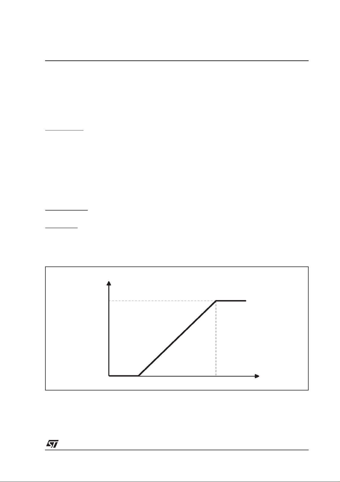
IN1 can accept two different types of inputs:
- an analog input between 0 and 5V (CF must be connected to set the PWM frequency) gives an analog
value of the Internal PWM duty cycle
- a digital input (CF must be grounded) gives directly the PWM
Figure 1 represents the Duty Cycle curve versus the IN1 analog voltage.
Figure 2 shows how to use the TD340 with an analog input or a digital input.
The speed control (or duty cycle) is achieved by the Low Side Drivers which impose the PWM function
while the cross-corresponding High Side MOSFETS is kept fully ON.
Direction Control:
IN2 accepts a digital value of the rotation direction.
Brake mode:
Brake mode is achieved by a zero level on the IN1 input.
The IN2 input selects low side or high side braking.
Brake mode is activated when the IN1 is at zero volt level for more than 200 us.
Figure 1 : Duty Cycle versus IN1 voltage
Duty Cycle
100%
0%
1.2V 3.6V IN1
Voltage
7/21
Page 8

Figure 2 : PWM Analog and Digital Modes
TD340
Vbatt
M
TD340
µP
5V
IN1
0V
ANALOG INPUT
+ CF (270pF)
PWM
PWM
CF
Vbatt
TD340
µP
M
PWM OUTPUT PWM OUTPUT
5V
IN1
0V
CF
DIGITALINPUT
+ CF GROUNDED
PWM
PWM
Active (synchronous) rectification for free-wheel current
A motor is an inductive load. When driven in PWM mode, motor current is switched on and off at the
25kHz frequency.When theMOS is switched off,currentcan not instantaneously dropto zero, a so-called
”free-wheel” current arises in the same direction than the power current. A path for this current must be
provided, otherwise high voltage could arise and destroy the component. The classical way to handle this
situation is to connect a diode in an anti-parallel configuration regarding to the MOS, so that current can
continue to flow through this diode, and finally vanishes by the means of ohmic dissipation, mainly in the
diode due to its 0.8V direct voltage. For high currents, dissipation can be an important issue (eg: 10A x
0.8V makes 8 W!). Furthermore, high speed diodes have to be used, and are expensive.
A more efficient way to handle this problem is to use the high side MOS as a synchronous rectifier. In this
mode, the upper MOS is switched ON when the lower one is switched OFF, and carries the free-wheel
current with much lower ohmic dissipation. Advantages are : one expensive component less (the fast
power diode), and more reliability due to the lower dissipation level.
However, we have to take care not to drive the two MOS simultaneously. To avoid transient problems
when the MOSare switched, a deadtime is inserted between the opening of one MOS, and the closing of
the otherone. In theTD340 device, the deadtimeis fixed to about 2.5 microseconds. Thisvalue is the time
between the commands of the gate drivers, not the deadtime between the actual MOS states because of
the rising and falling times of the gate voltages (due to capacitance), and the MOS characteristics. The
actual value of the deadtime for a typical configuration is about 1.5 microseconds.
Figure 3 shows the synchronous rectification principle
Table 1 summarizes the status of the Mosfets (and the speed and direction ofthe motor) according to the
Inputs (IN1 and IN2) status in analog and logic modes.
8/21
Page 9

TD340
Figure 3 : Synchronous Rectification Principle
ex1:
Speed: PWM=x%
No synchronousrectification
1-x%
FULL
OFF
PWM
M
x%
FULL
ON
FULL
OFF
HIGH DISSIPATION
THROUGH FREE WHEEL DIODE!
Table 1 : Function Table in Digital and Analog Modes
Stby
State
Disable
State
IN1 (V)
IN2
(V)
digital analog Q1L Q1H Q2L Q2H
Mosfets Status
ex2:
Speed: PWM=x%
With synchronousrectification - TD340
1-x%
PWM
FULL
ON
M
PWM
x%
LOW DISSIPATION
THROUGH LOW Rdson!
Comments
FULL
OFF
1 X X X X OFF OFF OFF OFF Motor Off in Standby Mode
X 1 X X X OFF OFF OFF OFF Motor Off in Disable Mode
0 0 0 idle 0 to 1.2 0 ON OFF ON OFF Motor Brake Low
0 0 0 idle 0 to 1.2 5 OFF ON OFF ON Motor Brake High
0 0 PWM 1.2 to 3.6 0 OFF ON PWM !PWM Motor x% Forward
0 0 PWM 1.2 to 3.6 5 PWM !PWM OFF ON Motor x% Backward
0 0 5 idle 3.6 to 5 0 OFF ON ON OFF Motor 100% Forward
0 0 5 idle 3.6 to 5 5 ON OFF OFF ON Motor 100% Backward
Notes:
- Standby state is active when STBY pin is pulled low
- Disable state is active when one of the following conditions is met: UVLO, OVLO, Reset, Watchdog Timeout.
9/21
Page 10

TD340
MOS drivers
Output drivers are designed to drive MOS with gate capacitance of up to 4 nF. A small resistor in serial
with gateinput is recommended to prevent spurious oscillations due to parasitic inductance inconjunction
with gate capacitance. Typical value of these resistors are from 10 to 100 ohms, depending on the MOS
characteristics.
Charge pump
To drivethehigh side MOS, theTD340 has to provide a voltage of about 10V higher that the power supply
voltage. The TD340 provides an internal charge pump which acts as a voltage tripling generator clamped
to 12V and allows the output of correct gate voltage with power voltage level as low as 6.5V. Its double
balanced structure ensures low EMI Ground Noise. The internal charge pump is used to achieve correct
voltage level at startup or static states.
An 5.6k resistor needs to be connected between OSC and GND for proper operation.
Bootstrap capacitors
To achieve dynamic driving up to 25kHz, it is necessary to support the internal charge pump with
bootstrap capacitors.
Bootstrap capacitorsare charged from Vbat when thelower MOS is ON. When the lower MOS isswitched
off and the upper one is switched ON, the bootstrap capacitor provides thenecessary current to the driver
in order to charge the gate capacitor to the right voltage level.
A design rule to select the bootstrap capacitor value is to choose ten times the gate capacitance.
For example, MOS with 4 nF gate capacitance will require bootstrap capacitors of about 47nF.
MOS gate discharge
The high side MOS are switched off with internal Gate to Source discharge (not Gate to Ground
discharge) to prevent the Gates from negative transient voltages.
Figure 4 : Typical waveforms on low and high side MOS gates.
Upper trace : High side MOS gate
Lower trace : Low side MOS gate
10/21
Page 11

TD340
Reversed battery active protection
In full H-bridge configuration, there is a risk in case of power voltage reversal due to the intrinsic diodes
inside the MOS. A passive protection solution is to wire a diode between the H-bridge and the power
supply. Disadvantages are voltage drop and power dissipation.
The TD340 provides support for reversed battery active protection.
An oscillator OSC output is available to allow proper command of a 5th MOS connected upside down.
The MOS must have low threshold voltage
In normal conditions, the MOS intrinsic diode supplies power to the driver at startup. When the TD340 is
started, the OSC output enables the MOS to switch on, providing lower voltage drop and lower power
dissipation.
In caseof reversed battery, the 5th MOS remains off, and no dangerous voltages can reach the driver nor
the power MOS.
The OSC oscillator can only supply a few mA. It must be loaded with a large impedance, typically 100pF
and 680k.
Figure 5 : Reversed Battery Active Protection Principle
because the oscillator output swing is about 6.5V.
Normal Conditions
Vbatt+6V
VbattOsc
1
2
3
TD340
4
VBATT
~Vbatt
2
M
3
REVERSED BATTERY
5
Driver isnot supplied
Vbatt
Osc
1
2
3
TD340
4
GND
MOSFET5
REMAINS
OFF
2
M
3
VBATT
GND
ALLMOSFETSAND DRIVERARE PROTECTED
UVLO and OVLO protections
The TD340 includes protections again overvoltage and undervoltage conditions.
Overvoltage is dangerous for the MOS and for the load due to possible excessive currents and power
dissipation.
Undervoltage is dangerous because MOS driving is no more reliable. MOS could be in linear mode with
high ohmic dissipation.
TD340 Under Voltage LockOut and Over Voltage LockOut features protect the system from no
operational power voltage. UVLO and OVLO thresholds are 6.2V and 20V. Hysteresis provides reliable
behavior near the thresholds.
During UVLO and OVLO, MOS are switched off (TD340 in disable state).
11/21
Page 12

TD340
Microcontroller support
For easy system integration, the TD340 provides the following functions:
- 5V regulator,
- reset circuit,
- watchdog circuit,
- standby mode,
- temperature indicator.
5V regulator
The TD340 provides a 5V regulated voltage at VOUT pin with amaximum current of 20mAover thewhole
Vbatt range (6.5 to 16V). Current can be up to 40 mA with nominal 12V Vbatt.
It is mandatory to connecta 220nF capacitor to the 5V output, even if the 5V output is not used, because
the 5V is internally used by the device. 220nF is the optimized value for the voltage regulator.
Reset circuit
The integratedsupervisor circuit resets themicro controller as soon as the voltage ofthe Micro Controller
decreases below 4.2V, and until the voltage of the micro controller has not passed above 4.3V.
RESET output is active low. It features an open drain with a internal 75k pull up resistor to internal 5V
which allows hardwired OR configuration.
Figure 6 : Reset Waveforms
Vout
Vthi
Vthd
Vccmin
Vreset
1V
zoom
tph l
t
t
12/21
Page 13

TD340
Watchdog circuit
An integrated Watchdog circuit resets the microcontroller when a periodic signal coming from the
microcontroller is missing after an externally adjustable Time out delay.
Watchdog timeout is adjustable by means of a capacitor Cwdbetween CWD pin and GND. This capacitor
should be placed as close as possible to the CWD pin.
Watchdog function can be inhibited by tying the CWD pin to ground.
Timeout range is from about 1ms to 1s, approximate value is given by:
Twd = 1 + (20 x Cwd) (Twd in ms, and Cwd in nF).
When the watchdog timeout triggers, the reset output is pulsed once low for 20 microseconds, and the
driver outputs are set to ground (MOS switched off). TD340 stays in disable state (MOS off) until pulses
appear again on WD pin.
Figure 7 : Watchdog waveforms
WDRESET
tip w
twd
treset
t
t
t
H1,H2,L1,L2
Temperature output
The TD340 provides a temperature indicator with the TEMP output.
TEMP voltage is 2.68V at 25°C with a temperature coefficient of -7.5mV/°C.
The goal of this function is to provide a rough temperature indication to the uP. It allows the system
designer to adapt the behavior of the application to the ambient temperature.
The TEMP output must be connected to a high impedance input. Maximum available current is 1uA.
13/21
Page 14

TD340
Standby mode
The TD340 can be put in standby mode under software control. When the STBY pin is driven low, the
MOS drivers are switched off and internal charge pump oscillator is stopped. The 5V regulator, the
watchdog and reset circuits are still active.
There is no pull up/down resistor on the STBY pin. STBY must not be left open.
Power consumption (not including the current drained from the 5V regulator) is reduced to about 200uA.
To achieve this standby current, the 5.6k resistor on the OSC pin has to be disconnected withan external
low power MOS controlled by the STBY signal (see figure 10 for an application example)
Standby mode should be only activated when IN1=IN2=0V and after that the motor is actually stopped
because thefour MOS are switched off. On exit from the standby mode, a delay of up to 20ms (depending
upon the bootstrap capacitor value) must be given before applying signals to the IN1 and IN2 inputs to
allow proper startup of the charge pump (it is also true for power-up). Figure 8 shows the voltage across
the Cb bootstrap capacitor at powerup or at standby exit as a function of time.
Figure 8 : Charge pump voltage at startup
Fig. 8a : Cb = 10nF
Fig. 8c : Cb = 100nF
Fig. 8b : Cb = 47nF
14/21
Page 15

TD340
PERFORMANCE CURVES
5V Regulator Voltage vs Output Current
5.1
5.0
Vbatt=16V
4.9
4.8
Vout(V)
4.7
Cout=22 0nF
4.6
4.5
0 102030405060
Vbatt=12V
Vbatt=8V
Vbatt= 6 V
Iout(mA)
Charge Pump Voltage vs Current
40
Vbatt=24 V
Vbatt=16V
Vbatt=12 V
Vcb (V)
35
30
25
20
5V Regulator Voltage vs Vbatt
5.1
5.0
4.9
4.8
Vout(V)
4.7
4.6
4.5
0 5 10 15 20 25
Vba tt (V)
Charge Pump Voltage vs Vbatt
40
35
30
25
ICb=0
Vcb (V)
20
Iload=20mA
Cout=220nF
15
10
Cb=10nF
5
0 20406080100120
Icb(µA)
High Side MOS Static Vgs vs Vbatt
13
12
11
10
Vgs (V)
9
8
7
6 8 10 12 14 16 18 20 22
Vbatt (V)
Vbatt= 6 .5V
15
10
5
5 10152025
ICb=60uA
Cb=10nF
Vbatt(V)
High Side MOS Static Vgs vs Temperature
12
11.5
11
Vgs (V)
10.5
10
-50 0 50 100 15 0
T(°C)
Vbatt=12V
15/21
Page 16

PERFORMANCE CURVES (continued) Vbatt= 12V, unless otherwise specified
TD340
Supply current
5
4.5
4
Icc (mA)
3.5
3
2.5
-50 0 50 100 150
T(°C)
Reset Threshold (decreasing)
4.4
4.3
4.2
Standby current
350
300
250
Istby(µA)
200
150
100
-50 0 50 100 15 0
T(°C)
Reset Threshold (increasing)
4.4
4.3
4.2
Vthd (V)
4.1
4.0
3.9
-50 0 50 100 150
Under Voltage Lockout
6.5
6.4
6.3
6.2
6.1
UVLO(V)
6.0
5.9
5.8
-50 0 50 100 150
T(°C)
T(°C)
Vthi (V)
4.1
4.0
3.9
-50 0 50 100 150
Over Voltage Lockout
22
21
20
OVLO(V)
19
18
-50 0 50 100 150
T(°C)
T(°C)
16/21
Page 17

TD340
PERFORMANCE CURVES (continued) Vbatt= 12V, unless otherwise specified
OSC Output Frequency
1.4
1.2
1.0
Fosc (MHz)
0.8
0.6
-50 0 50 100 150
T(°C)
High Side Driver output Current (source)
100
80
Deadtime between High and Low Drivers
3.8
3.6
3.4
no load
3.2
td (µs)
3
2.8
2.6
2.4
-50 0 50 100 150
T(°C)
Low Side Driver output Current (source)
100
80
60
Iouth_src (mA)
40
20
-50 0 50 100 150
T(°C)
High Side Driver output Current (sink)
14 0
12 0
10 0
Iouth_sink(mA)
80
60
-50 0 50 100 150
T(°C)
60
Ioutl_src (mA)
40
20
-50 0 50 100 15 0
T(°C)
Low Side Driver output Current (sink)
140
120
100
Ioutl_sink (mA)
80
60
-50 0 50 10 0 15 0
T(°C)
17/21
Page 18

TD340
APPLICATION CIRCUIT DIAGRAMS
The following schematics show typical application circuits. The first one is a simple,standalone system,
while the other one is µC driven and includes advanced features like standby mode and reversed battery
active protection.
Simple standalone system
Figure 9 shows a basic use of the TD340. The speed is controlled with a simple adjustable resistor.
Direction is controlled with a switch.
Internal PWM generator is used, frequency is set by the capacitor C3.
Note that the C2 capacitor (220nF) is included because it is needed by the internal TD340 circuit.
Interface lines for microcontroller are not used:
Standby is tied to 5V (Vout),
WD and CWD are tied to ground,
Reset and Temperature outputs are left unconnected.
Reversed battery protection is provided by the means of the diode D2.
Transistors Q1H, Q1L, Q2H, Q2L are to be chosen depending on the motor characteristics.
For example, STP30NE03L are 30V, 30A devices with gate capacitance of about 1nF. For these MOS,
22nF bootstrap capacitors are adequate.
Resistors R1 to R4 are used to control the rise and fall times on the MOS gates, and are also useful to
avoid oscillation of the gate voltage due to the parasitic inductance of lines in conjunction with the gate
capacitance. Typical values for resistors R1 to R4 are from 10 to 100 ohms.
Capacitor C6 is used to store energy and to filter the voltage across the bridge.
Applications:
Small domestic motorized equipments, battery-powered electrical tools, ...
Complete, µC driven system
The next schematic (figure 10) shows a complete system driven by a µC.
The auto-reload timer feature of ST6 µC family is used to easily generate the PWM command signal
(TD340 internal generator is not used, CF pin is connected to ground).
Transil diode D3 can be added as a security to avoid overvoltage transients if the MOS are all driven off
when the motor is running. For example, it can happen if TD340 is put in standby or disable state while
motor is running.
Applications:
- Automotive: advanced window lift systems, wiper systems, ...
- Industrial: battery-powered motor systems, electric door opening, ...
18/21
Page 19

TD340
Figure 9: Simple Standalone System
.
C6
470uF
+
+12V
Q1H
D1
MOSFET N
Load
Q2H
MOSFET N
C4 22nF
C5 22nF
R1 22
R2 22
Q1L
MOSFET N
GND
Q2L
MOSFET N
R3 22
R4 22
Q1L, Q1H, Q2L, Q2H: STP30NE03L
R5
5.6k
121113
14
15
16
17
18
19
20
Cb1
Osc
TD340
Vbat
Vout
12435
H1
Reset
S1
Cwd
H2
Cb2
Stby
Wd
6
7910
S2
Temp
8
L2
In1
L1
In2
Cf Gnd
U1
C3
270pF
C2
220nF
C1
+
10uF
S1
P1
10k
19/21
Page 20

Figure 10: Complete, µC Driven System
TD340
+Vbatt
Optionnal
R6
D1
680k
1N4148
Optionnal
Q3
MOSFET NC9
D2
1N4148
100pF
C4 47nF
D3
C6
470uF
+
Q1H
MOSFET N
Q2H
MOSFET N
C5 47nF
R1 100
R2 100
Motor
R3 100
Q1L
MOSFET N
GND
Q2L
MOSFET N
Q4
R4 100
5.6k
R5
BS170
Optionnal
Q3: STP60NE06L
Q1L, Q1H, Q2L, Q2H: STP60NE06
SW1
OPEN
SW2
CLOSE
121113
14151617181920
S1
H1
Cb1
Osc
TD340
Vbat
Vout
Reset
Cwd
12435
C1
10uF
+
Cb2
Stby
Wd
6
XT1
L1
L2S2H2
In1
In2
Temp
7910
8
Cf Gnd
U1
C3
100pF
C2
220nF
C8C7
XT1, C7, C8: see ST6252 datasheet
12111379
10
141516
NMI
PC3
PC2
ST6252
PB0
12435
Vpp/Test
PB2
Reset
PB3
OSCin
OSCout
PB7
PB6
6
PA5
Vdd
U2
Vss PA4
8
20/21
Page 21

TD340
PACKAGE MECHANICAL DATA
20 PINS - PLASTIC MICROPACKAGE (SO)
Dim.
Millimeters Inches
Min. Typ. Max. Min. Typ. Max.
a1 0.254 0.010
B 1.39 1.65 0.055 0.065
b 0.45 0.018
b1 0.25 0.010
D 25.4 1.000
E 8.5 0.335
e 2.54 0.100
e3 22.86 0.900
F 7.1 0.280
I 3.93 0.155
L 3.3 0.130
Z 1.34 0.053
Information furnished is believed to be accurate and reliable. However, STMicroelectronics assumes no responsibility for the
consequences of use of such information nor for any infringement of patents or other rights of third parties which may result from
its use. No license is granted by implication or otherwise under any patent or patent rights of STMicroelectronics. Specifications
mentioned in this publication are subject to change without notice. This publication supersedes and replaces all information
previously supplied. STMicroelectronics products are not authorized for use as critical components in life suppo rt devices or
systems withoutexpress written approval of STMicroelectronics.
Australia - Brazil - China - Finland - France - Germany - Hong Kong - India - Italy - Japan - Malaysia - Malta - Morocco
The ST logo is a registered trademark of STMicroelectronics
2000 STMicroelectronics - Printed in Italy - All Rights Reserved
STMicroelectronics GROUP OF COMPANIES
Singapore - Spain - Sweden - Switzerland - United Kingdom
http://www.st.com
21/21
 Loading...