

Page 1
®
.
THREE POWER IGBT/MOS OR PULSE
TRANSFORMER DRIVERS
.
CURRENT SENSE COMPARATOR WITH
1ms INHIBITION TIME FUNCTION
.
INSTANTANE OUS S IGNA L T RANSMI S SION
.
0.6 Amp PER CHANNEL PEAK OUTPUT
CURRENT CAPABILITY
.
LOW OUTPUT IMPEDANCE TYP : 7Ω at
200mA
.
CMOS/LSTTL COMPATIBLE INVERTING INPUT WITH HYSTERESIS
.
13V TO 16V SINGLE SUPPLY OPERATION
.
UNDER VOLTAG E LOCK OUT (12.5V)
.
CURRENT AMPLIFIER
.
LOW BIAS CURRENT TYP : 1.5mA
.
DURING POWER UP NO RANDOM OUTPUT
STATE
.
ENHANCED LATCH-UP IMMUNITY
.
CHANNEL PA RALLELING CAPA BILIT Y
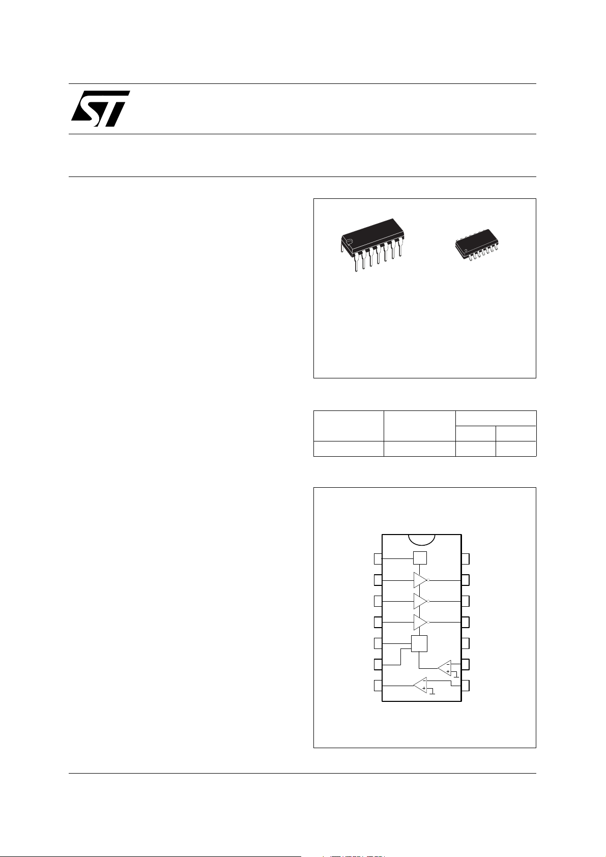
TD300
15V TRIPLE IGBT /MO S DRI VER
N
DIP14
(Plastic Package)
ORDER CO DES
Part Number
TD300I -40
(Plastic Micropackage)
Temperature
Range
o
C, +105oC ••
D
SO14
Package
ND
DESCRIPTIO N
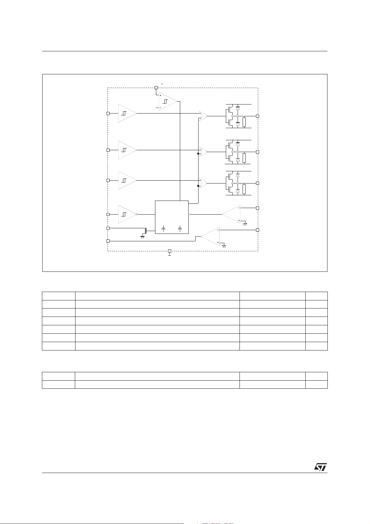
The TD300 is designed to drive one, two or three
Power IGBT/MOS and has driving capability for
pulse transformer. So it is perfectly suited to interface control IC with Power Switches in low side or
half-bridge configuration.
The typical application shown figure 1 implements
the TD300 in a pulse controlled half-bridge drive.
Positive and negative pulses are applied to the
pulse transformer to charge and discharge the
IGBT/MOS gate capacitance. More sophisticated
secondary circuits provide low impedance gate
drive and short-circuit prot ection as shown in application note AN461.
On Figure 2, TD300 is implemented as a low side
driver in a typical 3 phase motor drive.
Figure 3 presents a general purpos e low side gate
drive.
In both case, the current amplifier provides interfacing between a sense resistor and an A/D
converter .
June 1998
PIN CONNECTIONS
V
CC
Input A
Input B
Input C
Enable
Alarm
OA Output
1
+
2
3
4
5
6
7
14
13
12
11
10
9
8
N.C.
Output A
Output B
Output C
GND
Sense input
OA input
1/8
Page 2
TD300
BLOCK DIAG RAM
15V
V
CC
1
2 - Input A
3 - Input B
4 - Input C
5 - Enable
6 - Alarm
7 - Current
Output
12.5V
Control Unit
tsi tAI
10
GND
13 - Output A
12 - Output B
11 - Output C
9 - Sense input
0V
8 - Current Input
0V
ABSOLUTE MAXIMUM RATINGS
Symbol Parameter Value Unit
V
CC
V
V
is
T
T
amb
T
stg
Supply Voltage 18 V
Input Voltage 0 to V
i
Sense Input Voltage -0.3 to V
Operating Junction Temperature -40 to 150
j
Operating Ambient Temperature -40 to 105
Storage Temperature Range -65 to 150
CC
CC
V
V
o
C
o
C
o
C
OPERAT ING CONDIT IONS
Symbol Parameter Value Unit
V
CC
Supply Voltage 13 to 16 V
INSTRUCTIONS FOR USE
1 - The TD300 supply voltage must be decoupled with a 1µF min. capacitor.
2 - If the application involving TD300 requires maximum output current capability,
this current must be pulsed : pulse width 1µsec, duty cycle 1% at T
2/8
amb
.
Page 3

ELECTRICAL CHARACT ERISTICS
V
= 15V, T
CC
Symbol Parameter Min. Typ. Max. Unit
I
CC
V
IH
V
IL
I
IH
I
IL
t
dH,teL
t
dL,teH
t
Ii
t
dd
V
sod
V
sid
V
dem
R
opd
V
hys
V
st
I
s
I
sh
t
A
V
ios
t
Ai
t
s
t
si
V
shys
V
icm
V
io
I
io
I
o
V
OL
V
OH
GBP Gain Bandwidth Product 1 MHz
A
vd
SR Slew Rate at Unity Gain (R
= 25oC (unless otherwise specified)
amb
Supply Current with Inputs in High State 1.5 2 mA
LOGIC INPUT (all inputs)
High Input Voltage 2 V
Low Input Voltage 0.8 V
High Input Current 10 pA
Low Input Current 10 pA
Propagation Delay (10% input to 10% output)
Output Delay
Output Delay
≤ T
T
min.
amb
≤ T
200
60
max.
400
400
Input Inhibiting Time 100 ns
Differential Delay Time Between Channels 20 ns
OUTPUT DRIVERS
Sourcing Drop Voltage (A/B/C outputs)
= 200mA 3
I
source
Sinking Drop Voltage (A/B/C outputs)
I
= 200mA 5
sink
Demagnetising Drop Voltage (A/B/C outputs)
I
= 100mA 2
demag.
Output Pull Down Resistor 47 kΩ
UNDERVOLTAGE LOCKOUT
Threshold Hysteresis 0.8 V
Internal Start Threshold 11.7 13.3 V
ALARM OUTPUT
Low Level Sinking Current
= 0.8V 5 35
V
O
High Level Sinking Current 500 nA
Alarm Output : Delay Time to Alarm Fall if Sense Input Triggered 500 ns
SENSE INPUT
Input Offset Voltage 20 mV
Inhibition Time if Sense Input Triggered 1 ms
Delay Time to Output Fall if Sense Input Triggered
All outputs inhibited 600
Inhibition Time of Sense Input 300 ns
Sense Hysteresis 40 mV
OPERATIONAL AMPLIFIER
Common Mode Input Voltage Range 0 to V
+
- 1.5 V
CC
Input Offset Voltage 10 mV
Input Offset Current 1 pA
Output Short Circuit Current (V
Low Level Output Voltage (V
High Level Output Voltage (V
= 100mV, Vo = 0V) 60 mA
id
= -100mV) 20 mV
id
= 100mV, RL = 100kΩ) 8.9 V
id
Open Loop Gain 60 dB
= 100kΩ, CL = 100pF, Vi = 3 to 7V) 0.6 V/µs
L
TD300
ns
V
V
V
mA
ns
3/8
Page 4

TD300
TIMING DIAGRAM
TIMING 1
Input
A/B/C
tdH
Output
A/B/C
TIMING 2
Input
A/B/C
tli
tdL
Output
A/B/C
Sense
Alarm
Enable
Under
Voltage
ts
tAi
tA
teL
teH
4/8
Page 5

TYPICAL APPLICATIONS
Figure 1 : THREE PHA SE MO TO R HI GH AND LO W SIDE DRI VE
15V
1mF
MCU signals
TD300
Pulse transformer
1/3 Fil-Mag 42Z4056
or 23Z284SMD
TD300
High Voltage
ON
Pulse controlled inputs
OFF
Level controlled input
enable
interrupt
AD converter
alarm
CONTROL
UNIT
Vz = 15V
3 Phases motor
15V
Rsense
5/8
Page 6

TD300
Figure 2 : THREE PHASE MOTOR LOW SIDE DRIVE
Vd
KEYBOARD
DISPLAY
Figure 3 : LOW SIDE DRIVE
ST6
µ
T1
L6380
B
U
F
P
F
E
R
+15V
1mF
L6380
L6380
T
D
3
0
0
Load Load Load
T2
T3
T4
T5
MOTOR
T6
6/8
Rsense
Page 7

PACKAGE MECHANICAL DATA
14 PINS - PLASTIC DIP
TD300
Dimensions
a1 0.51 0.020
B 1.39 1.65 0.055 0.065
b 0.5 0.020
b1 0.25 0.010
D 20 0.787
E 8.5 0.335
e 2.54 0.100
e3 15.24 0.600
F 7.1 0.280
i 5.1 0.201
L 3.3 0.130
Z 1.27 2.54 0.050 0.100
Min. Typ. Max. Min. Typ. Max.
Millimeters Inches
7/8
Page 8

TD300
PACKAGE MECHANICAL DATA
14 PINS - PLASTIC MICRO PACKAGE (SO )
Dimensions
Min. Typ. Max. Min. Typ. Max.
Millimeters Inches
A 1.75 0.069
a1 0.1 0.2 0.004 0.008
a2 1.6 0.063
b 0.35 0.46 0.014 0.018
b1 0.19 0.25 0.007 0.010
C 0.5 0.020
c1 45
o
(typ.)
D 8.55 8.75 0.336 0.334
E 5.8 6.2 0.228 0.244
e 1.27 0.050
e3 7.62 0.300
F 3.8 4.0 0.150 0.157
G 4.6 5.3 0.181 0.208
L 0.5 1.27 0.020 0.050
M 0.68 0.027
S8
Information furnished is believed to be accurate and reliable. However, STMicroelectronics assumes no responsibility for the
consequences of use of such information nor for any infringement of patents or other rights of third parties which may result from
its use. No license is granted by implication or otherwise under any patent or patent rights of STMicroelectronics. Specifications
mentioned in this publication are subject to change without notice. This publication supersedes and replaces all information
previously supplied. STMicroelectronics products are not authorized for use as critical components in life support devices or systems
without express written approval of STMicroelectronics.
© The ST logo is a trademark of STMicroelectronics
o
(max.)
8/8
© 1998 STMicroelectronics – Printed in Italy – All Rights Reserved
STMicroelectronics GROUP OF COMPANIES
Australia - Brazil - Canada - China - France - Germany - Italy - Japan - Korea - Malaysia - Malta - Mexico - Morocco
The Netherlands - Singapore - Spain - Sweden - Switzerland - Taiwan - Thailand - United Kingdom - U.S.A.
 Loading...