

Page 1

NTE49 (NPN) & NTE50 (PNP)
Silicon Complementary Transistors
General Purpose, High Voltage Amp, Driver
Description:
The NTE49 (NPN) and NTE50 (PNP) are silicon complementary transistors in a TO202 type case
designed for general purpose, high voltage amplifier and driver applications.
Features:
D High Collector Breakdown Voltage: V
D High Power Dissipation: P
= 10W @ TC = +25C
D
(BR)CEO
Absolute Maximum Ratings:
Collector−Emitter Voltage, V
Collector−Base Voltage, V
Emitter−Base Voltage, V
Continuous Collector Current, I
Total Power Dissipation (T
CEO
CB
EB
C
= +25C), P
A
D
Derate Above 25C 8mW/C.......................................................
Total Power Dissipation (TC = +25C), P
D
Derate Above 25C 80mW/C......................................................
Operating Junction Temperature Range, T
Storage Temperature Range, T
stg
Thermal Resistance, Junction−to−Case, R
J
thJC
Thermal Resistance, Junction−to−Ambient, R
= 100V Min @ IC = 1mA
thJA
100V.....................................................
120V........................................................
4V...........................................................
2A......................................................
1W..............................................
10W............................................
−55 to +150C..................................
−55 to +150C..........................................
12.5C/W....................................
125C/W..................................
Rev. 5−13
Page 2
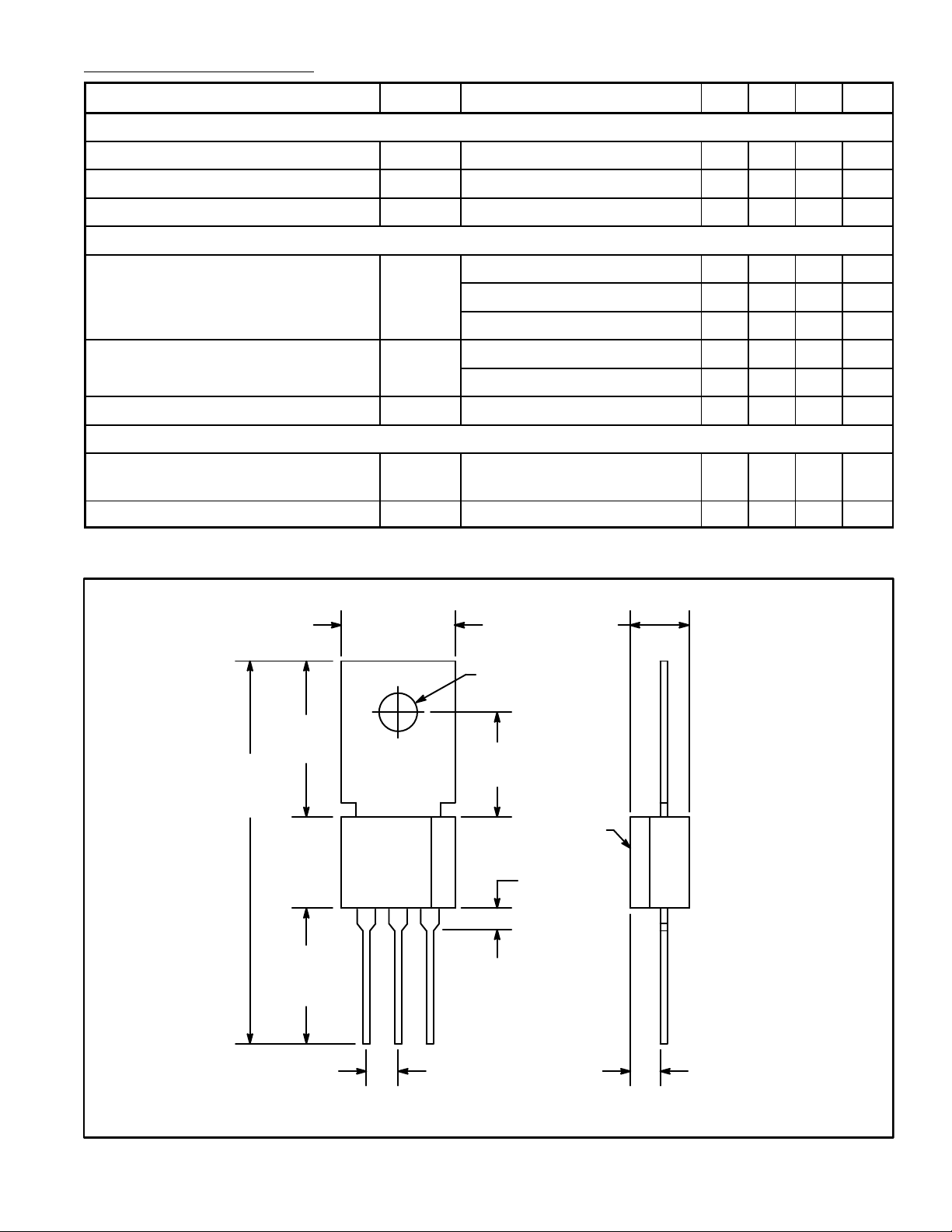
Electrical Characteristics: (TA = +25C unless otherwise specified)
Parameter Symbol Test Conditions Min Typ Max Unit
OFF Characteristics
Collector−Emitter Breakdown Voltage V
Emitter−Base Breakdown Voltage V
Collector Cutoff Current I
(BR)CEOIC
(BR)EBOIE
CBO
= 1mA, IB = 0 100 − − V
= 100A, IC = 0 4 − − V
VCB = 40V, IE = 0 − − 100 nA
ON Characteristics (Note 2)
DC Current Gain h
FE
IC = 50mA, VCE = 1V 80 125 −
IC = 250mA, VCE = 1V 60 100 −
IC = 500mA, VCE = 1V − 55 −
Collector−Emitter Saturation Voltage V
CE(sat)IC
= 250mA, IB = 10mA − 0.18 0.4 V
IC = 250mA, IB = 25mA − 0.1 − V
Base−Emitter ON Voltage V
BE(on)IC
= 250mA, VCE = 5V − 0.74 1.2 V
Small−Signal Characteristics
Current Gain−Bandwidth Product f
T
IC = 250mA, VCE = 5V,
f = 100MHz, Note 1
Output Capacitance C
ob
VCB = 10V, IE = 0, f = 100kHz − 6 12 pF
Note 2. Pulse Test: Pulse Width 300s, Duty Cycle 2%.
50 150 − MHz
C
.500
(12.7)
1.200
(30.48)
Ref
.300
(7.62)
.400
(10.16)
Min
EBC
.100 (2.54) .100 (2.54)
.132 (3.35) Dia
.325
(9.52)
.180 (4.57).380 (9.56)
.070 (1.78) x 45
Chamf
.050 (1.27)
 Loading...