

Page 1
TCA 305
TCA 355
Proximity Switch
Features
● Lower open-loop current consumption; IS < 1 mA
● Lower output saturation voltage
● The temperature dependence of the switching
distance is lower and compensation of the resonant
TC
circuit
● The sensitivity is higher, so that larger switching
distances are possible and coils of a lower quality can
be used
● The switching hysteresis remains constant as regards
temperature, supply voltage and switching distance
● The TCA 305 even functions without external
integrating capacitor. With an external capacitor (or
with RC combination) good noise immunity can be
achieved
(temperature coefficient) is easier
TCA 305
TCA 355
Bipolar IC
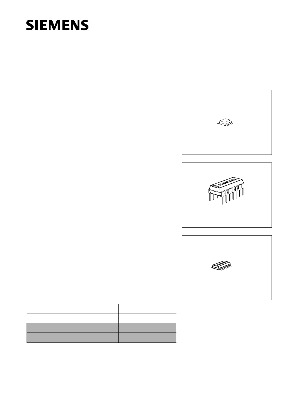
P-DSO-8-1
● The outputs are temporarily short-circuit proof (approx.
10 s to 1 min depending on package)
● The outputs are disabled when VS < approx. 4.5 V and
are enabled when the oscillator stabilizes
(from V
● Higher switching frequencies can be obtained
● Miniature package
Type Ordering Code
TCA 305 A Q67000-A2291
■
S min = 5 V)
Package
P-DIP-14-1
TCA 305 G Q67000-A2305 P-DSO-14-1 (SMD)
TCA 355 G Q67000-A2444 P-DSO-8-1 (SMD)
■ Not for new design
P-DIP-14-1
P-DSO-14-1
Semiconductor Group 1
01.96
Page 2
TCA 305
TCA 355
TCA 305 A
TCA 305 G
TCA 355 G
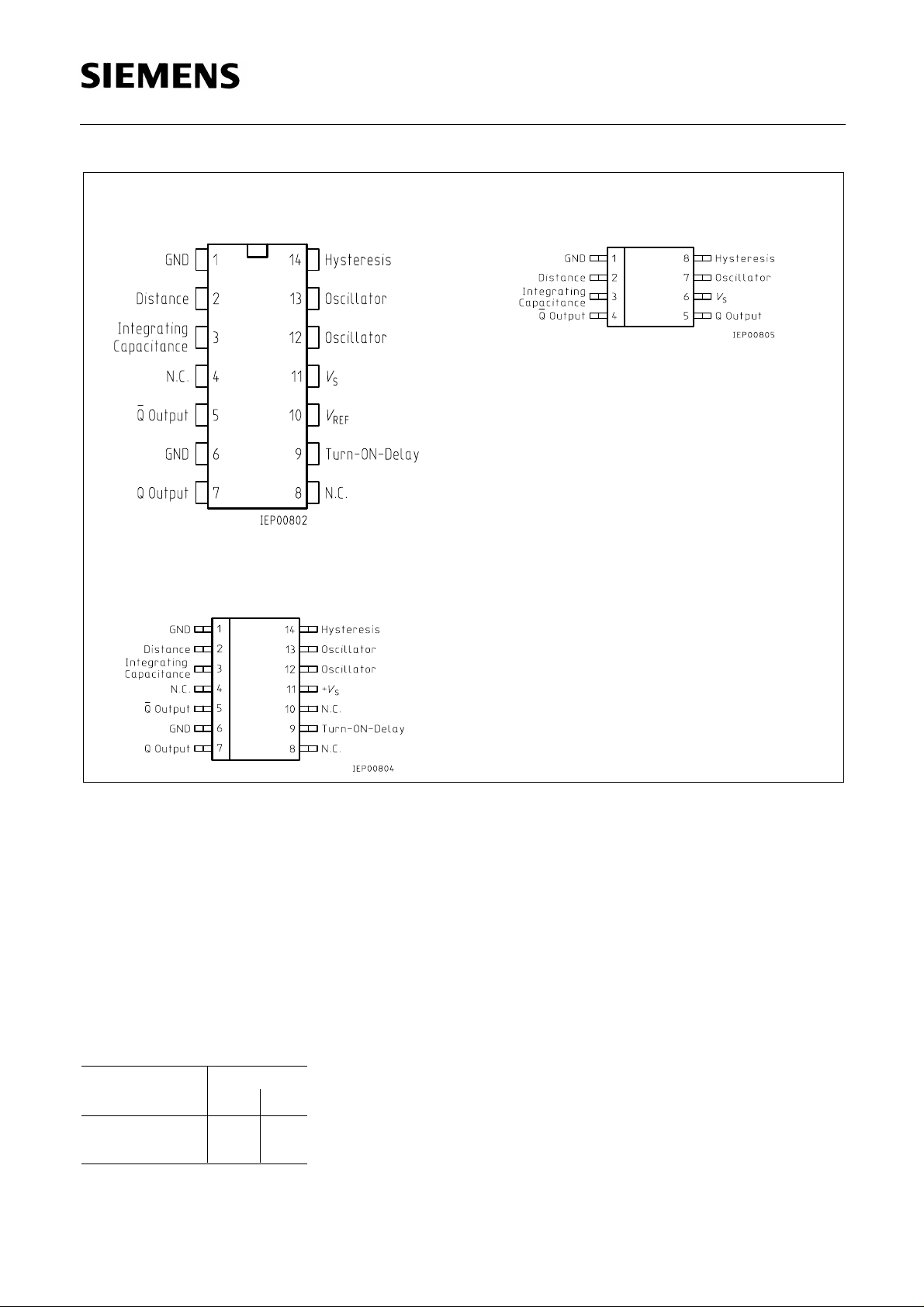
Pin Configurations (top view)
The devices TCA 305 and TCA 355 contain all the functions necessary to design inductive
proximity switches. By approaching a standard metal plate to the coil, the resonant circuit is
damped and the outputs are switched.
Operation Schematic: see TCA 205
The types TCA 305 and TCA 355 have been developed from the type TCA 205 and are outstanding for the following characteristics:
Logic Functions
Oscillator Outputs
Q
not damped
damped
H
L
L
H
Semiconductor Group 2
Page 3
TCA 305
TCA 355
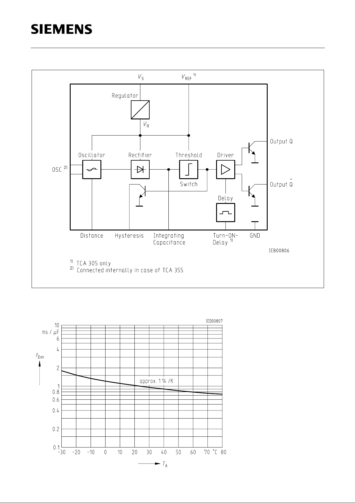
Block Diagram
Standard Turn-ON Delay Referred to T
A = 25 ˚C
Semiconductor Group 3
Page 4
TCA 305
Ω
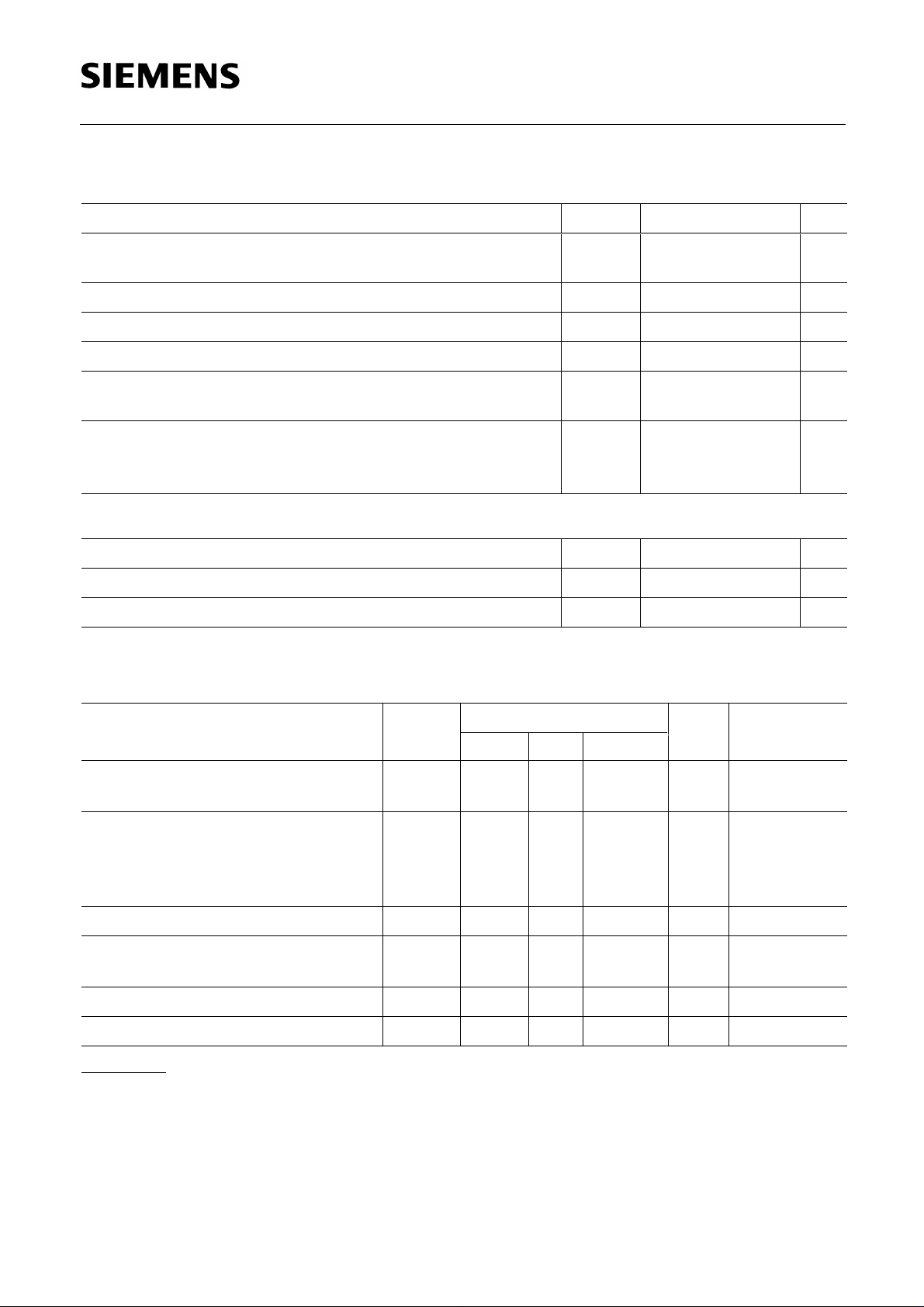
Absolute Maximum Ratings
Parameter Symbol UnitLimit Values
TCA 355
Supply voltage
Output voltage
VS
VQ
35
35
V
V
Output current IQ mA50
Distance, hysteresis resistance RDi, RHy Ω0
Capacitances C
Junction temperature
Storage temperature range
I, CD µF5
Tj
Tstg
150
– 55 to 125
˚C
˚C
Thermal resistance
system - air TCA 305 A
TCA 305 G
th SA
R
Rth SA
85 (135)
140 (200)
2)
2)
K/W
K/W
Operating Range
Supply voltage VS V
5 to 30
3)
Oscillator frequency fOSC MHz0.015 to 1.5
Ambient temperature TA ˚C– 25 to 85
Characteristics
S = 12 V, TA = – 25 to 85 ˚C
V
Parameter
Open-loop
current consumption
Reference voltage
1)
L-output voltage
per output
VREF
VQ L
VQ L
VQ L
Limit ValuesSymbol
typ.min. max.
0.6 0.9
3.2
0.04
0.10
0.22
(1.0)
0.15
0.35
0.75
2)
Unit Test
Condition
mA outputs openIS
V
V
V
V
REF< 10 µA
I
Q L = 5 mA
I
Q L = 25 mA
I
Q L = 50 mA
I
H-output current per output 10 µA VQ H = 30 VIQ H
Threshold at 3
Hysteresis at 3
Turn-ON delay
VS 3
VHy
1)
2.1
0.50.4 0.6
600– 25 % – 25 % ms/µF TA = 25 ˚CtD ON
V
V
Switching frequency w/o CI 5 kHzfS
1)
TCA 305 only
2)
Values in parenthesis apply to TCA 355 only
3)
Operation at voltages less than 5 V (between approx. 2.5 and 5 V) is possible, if VREF is connected to VS. In
this case VREF is no longer internally stabilized. Additionally, the pin "turn-on delay" is to be applied as follows:
If no turn-on delay is needed, this pin has to be connected to VS. If, however, a turn-on delay is required, the
charge current for DD has to be adjusted with an external resistor between this pin and VS (recommended
value 390 k ).
Semiconductor Group 4
Page 5
TCA 305
TCA 355
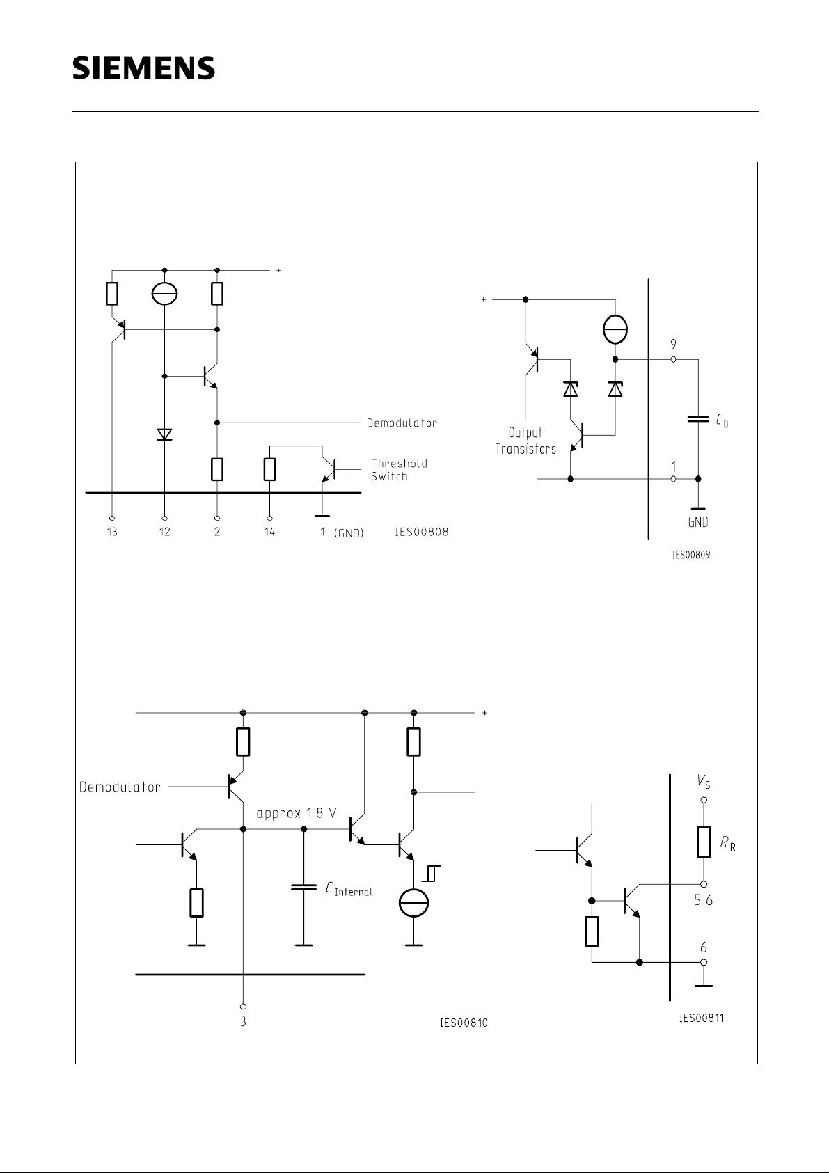
Oscilator
Turn-ON Delay for TCA 305 A; G
Integrating Capacitor Outputs
Schematic Circuit Diagram
Semiconductor Group 5
Page 6
TCA 305
TCA 355
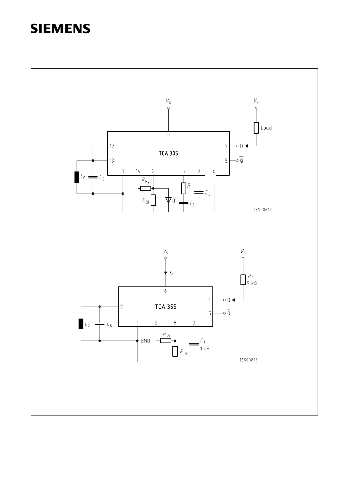
Application Circuit
Semiconductor Group 6
Page 7
TCA 305
Ω
L
R
Ω
Ω
Ω
Ω
Ω
TCA 355
L0, C0 Resonant circuit
Hy Hysteresis adjustment
R
Di Distance adjustment
R
D Temperature compensation of the resonant circuit; possibly with series
resistance for the purpose of adjustment. The diode is not absolutely necessary.
Whether it is used or not depends on the temperature coefficient of the resonant
circuit.
I; CI Integration element. At pin 3 (integrating capacitance) we recommend a
R
capacitor of typ. 1 nF. To increase noise immunity this capacitor can be
substituted by an RC circuit with, e.g., R
D Delay capacitor
C
Dimensioning Examples in Accordance with CENELEC Standard (flush)
I = 1 M and CI = 10 nF.
Ferrite pot core
Number of turns
Cross section of wire
0
C0 (STYROFLEX®)
OSC
f
Sn
A (Metal)
D
C
M 12 M 18 M 30
M 33 (7.35 × 3.6) mm
100
0.1 CuL
µH
206
1000 pF
appr. 350 kHz
4 mm
8.2 k + 330
100 nF
N 22 (14.4 × 7.5) mm
80
× 0.05
20
µH
268
1.2 nF
appr. 280 kHz
8 mm
33 k
100 nF
N 22 (25 × 8.9) mm
100
× 0.1
10
585
3.3 nF
appr. 115 kHz
15 mm
22 k + 2.7 k
100 nF
µH
Semiconductor Group 7
 Loading...