

Page 1
TC962
V
DD
1
2
3
4
5
6
7
8
16
13
12
11
10
9
NC
GND
C
OSC
NC
15
14
NC
NC
NC
TC962COE
NC
NC
Zener
Cathode
NC
FREQ x 2
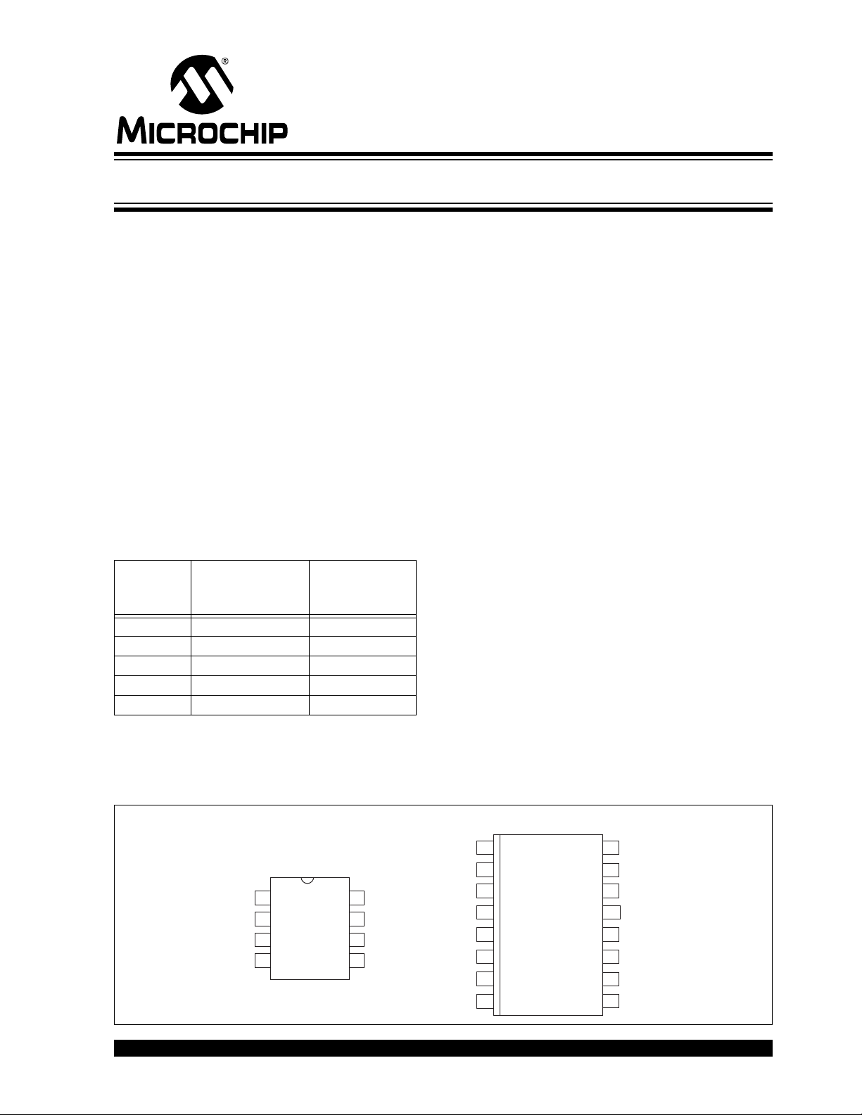
16-Pin SOIC Wide
C
+
C
–
V
OUT
1
2
3
4
8
7
6
5
FREQ x 2
GND
TC962CPA
TC962EPA
TC962IJA
TC962MJA
C
+
C
–
V
OUT
8-Pin CERDIP
8-Pin DIP
•
Zener
Cathode
C
OSC
V
DD
High Current Charge Pump DC-to-DC Converter
Features:
• Pin Compatible With TC7662/ICL7662/SI7661
• High Output Current 80 mA
• No External Diodes Required
• Wide Operating Range 3V to 18V
• Low Output Impedance 28 Typ.
• No Low Voltage Terminal Required
• Application Zener On-Chip
• OSC Frequency Doubling Pin Option for Smaller
Output Capacitors
Applications:
• Laptop Computers
•Disk Drives
• Process Instrumentation
• P-Based Controllers
Device Selection Table
Part
Number
Package
TC962COE 16-Pin SOIC Wide 0°C to +70°C
TC962CPA 8-Pin Plastic DIP 0°C to +70°C
TC962EPA 8-Pin Plastic DIP -40°C to +85°C
TC962IJA 8-Pin CERDIP -25°C to +85°C
TC962MJA 8-Pin CERDIP -55°C to +1 25°C
Operating
Temp.
Range
General Description:
The TC962 is an advanced version of the industry
standard TC7662 high voltage DC-to-DC converter.
Using improved design techniques and CMOS
construction, the TC96 2 can sourc e as much as 80 mA
versus the 7662’s 20 mA capability.
As an inverter, the TC962 can put out voltages as high
as 18V and as low as 3V without the need for external
diodes. The output impedance of the device is a low
28 (with the proper capacitors), voltage conversion
efficiency is 99.9%, and power conversion efficiency is
97%.
The low voltage terminal (pin 6) required in some
TC7662 applications has been eliminated. Grounding
this terminal will double the oscill ator frequency fro m 12
kHz to 24 kHz. This will allow the use of smaller
capacitors for the same output current and ripple, in
most applications. Only two external capacitors are
required for inverter applications. In the event an
external clock is needed to drive the TC962 (such as
paralleling), driving this pin directly will cause the
internal oscillator to sync to the external clock.
Pin 1, which is used as a test pin on the 7662, is a
voltage reference Zener on the TC962. This Zener (6.4V
at 5 mA) has a dynamic impedance of 12 and is
intended for use where the TC962 is supplying current to
external regulator circuitry and a reference is needed for
the regulator circuit. (See Section 3.0 “Applications
Information” Applications Information).
The TC962 is compatible with the LTC1044, SI7661
and ICL7662. It should be used in designs that require
greater power and/or less input to output voltage drop.
It offers superior performance over the ICL7660S.
Package Type
2001-2012 Microchip Technology Inc. DS21484D-page 1
Page 2
TC962
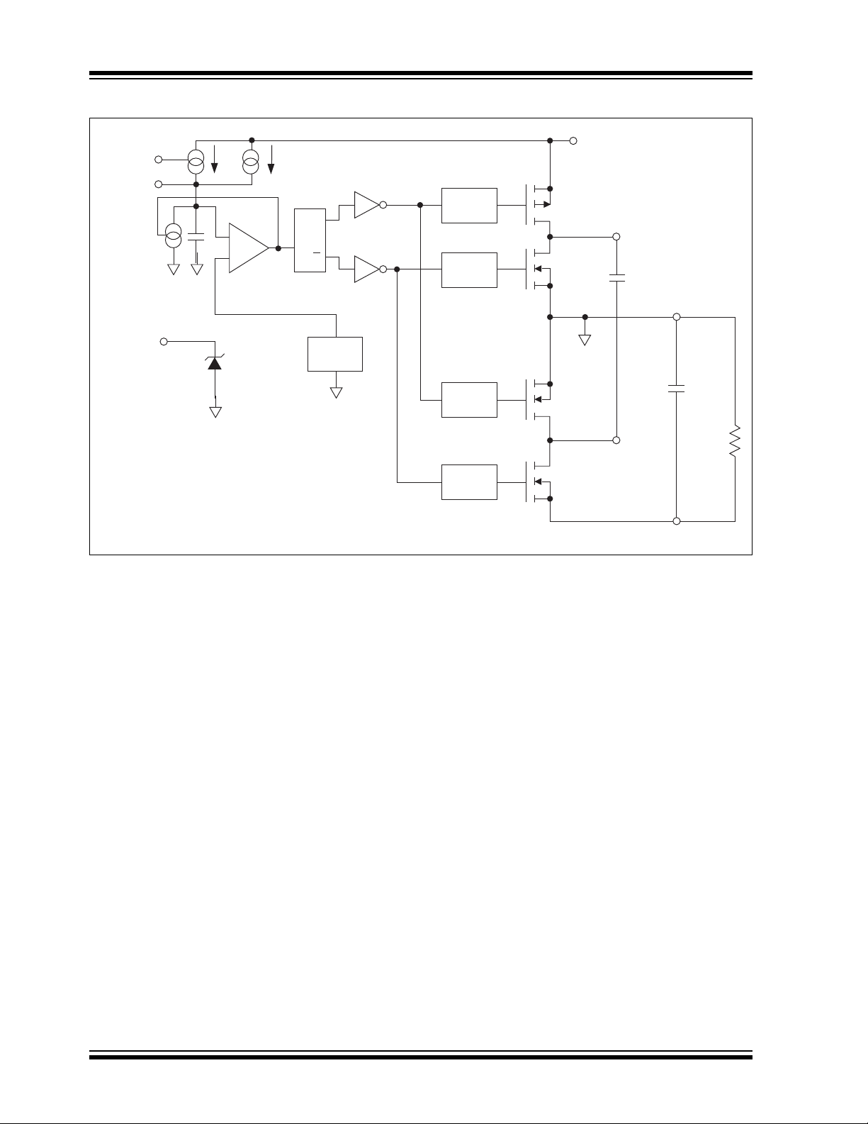
Functional Block Diagram
FREQ x 2
OSC/C
Timing
Zener
Cathode
6
–
7
I I
+
–
Comparator
with Hysteresis
1
6.4V
8
V
DD
TC962
Level
Q
F/F
C
Q
V
REF
Shift
Level
Shift
Level
Shift
P SW1
N SW4
N SW2
2
+
CAP
C
P
External
OUT
+
GND
3
+
C
R
EXT
Level
Shift
N SW3
4
CAP
–
5
V
OUT
R
L
DS21484D-page 2 2001-2012 Microchip Technology Inc.
Page 3
TC962
1.0 ELECTRICAL
CHARACTERISTICS
Absolute Maximum Ratings*
Supply Voltage (VDD to GND)..............................+18V
Input Voltage Any Pin
.........................(V
Current Into Any Pin...........................................10 mA
ESD Protection ................................................±2000V
Output Short Circuit ........... Continuous (at 5.5V Input)
Package Power Dissipation (T
SOIC.......................................................760 mW
PDIP........................................................730 mW
CERDIP ..................................................800 mW
Package Thermal Resistance
CERDIP, R
PDIP, R
J-A
............................................140°C/W
J-A
Operating Temperature Range
CPA, COE .......................................0°C to +70°C
IJA................................................-25°C to +85°C
EPA .............................................. -40°C to +85°C
MJA............................................-55°C to +125°C
Storage Temperature Range .............-65°C to +150°C
+0.3) to (VSS -0.3) (Note 1)
DD
70°C)
A
.........................................90°C/W
*Stresses above those listed under “Absolute
Maximum Ratings” may cause permanent damage to
the device. Thes e are stress ratin gs only and functional
operation of the devic e at these or an y other con ditions
above those indicated in the operation sections of the
specifications is not implied. Exposure to Absolute
Maximum Rating conditions for extended periods may
affect device reliability.
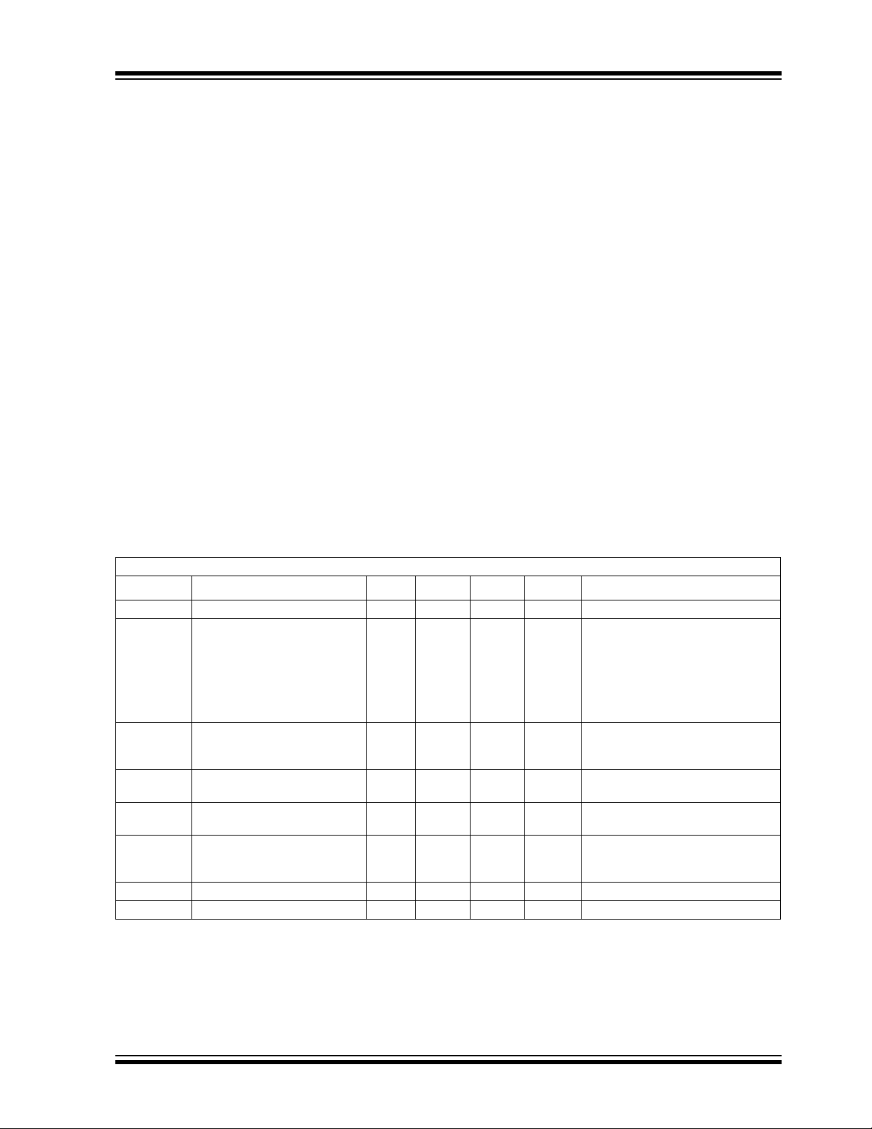
TC962 ELECTRICAL SPECIFICATIONS
Electrical Characteristics: VDD = 15V, TA = 25°C (See Figure ) unless otherwise noted.
Symbol Parameter Min Typ Max Units Tes t Conditions
V
DD
I
S
R
O
F
OSC
P
EFF
V
DEF
V
Z
Z
ZT
Note 1: Connecting any input terminal to voltages greater than V+ or less than GND may cause destructive latch-up. It is recommended that no
Supply Voltage 3 — 18 V
Supply Current
V
= 15V
DD
= 5V
V
DD
Output Source
Resistance
Oscillator Frequency —
Power Efficiency 93
Voltage Efficiency 99
Zener Voltage 6.0 6.2 6.4 V IZ = 5 mA
Zener Impedance — 12 — IL = 2.5 mA to 7.5 mA
inputs from sources operating from external supplies be applied prior to “power-up” of the TC962.
—
—
—
—
—
—
—
—
—
—
—
—
—
96
—
510
560
650
190
210
210
32
35
—
12
24
97
—
99.9
—
—
—
700
—
—
—
—
—
37
40
50
—
—
—
—
—
—
—
AR
I
kHz Pin 6 Open
%RL = 2 k
%RL =
=
L
T
= +25°C
A
70°C
0 T
A
= +25°C
70°C
A
125°C
A
125°C
A
-55°C T
T
A
0 T
-55°C T
= 20 mA, VDD = 15V
L
= 80 mA, VDD = 15V
I
L
= 3 mA, VDD = 5V
I
L
Pin 6 GND
Over temperature range
2001-2012 Microchip Technology Inc. DS21484D-page 3
Page 4
TC962
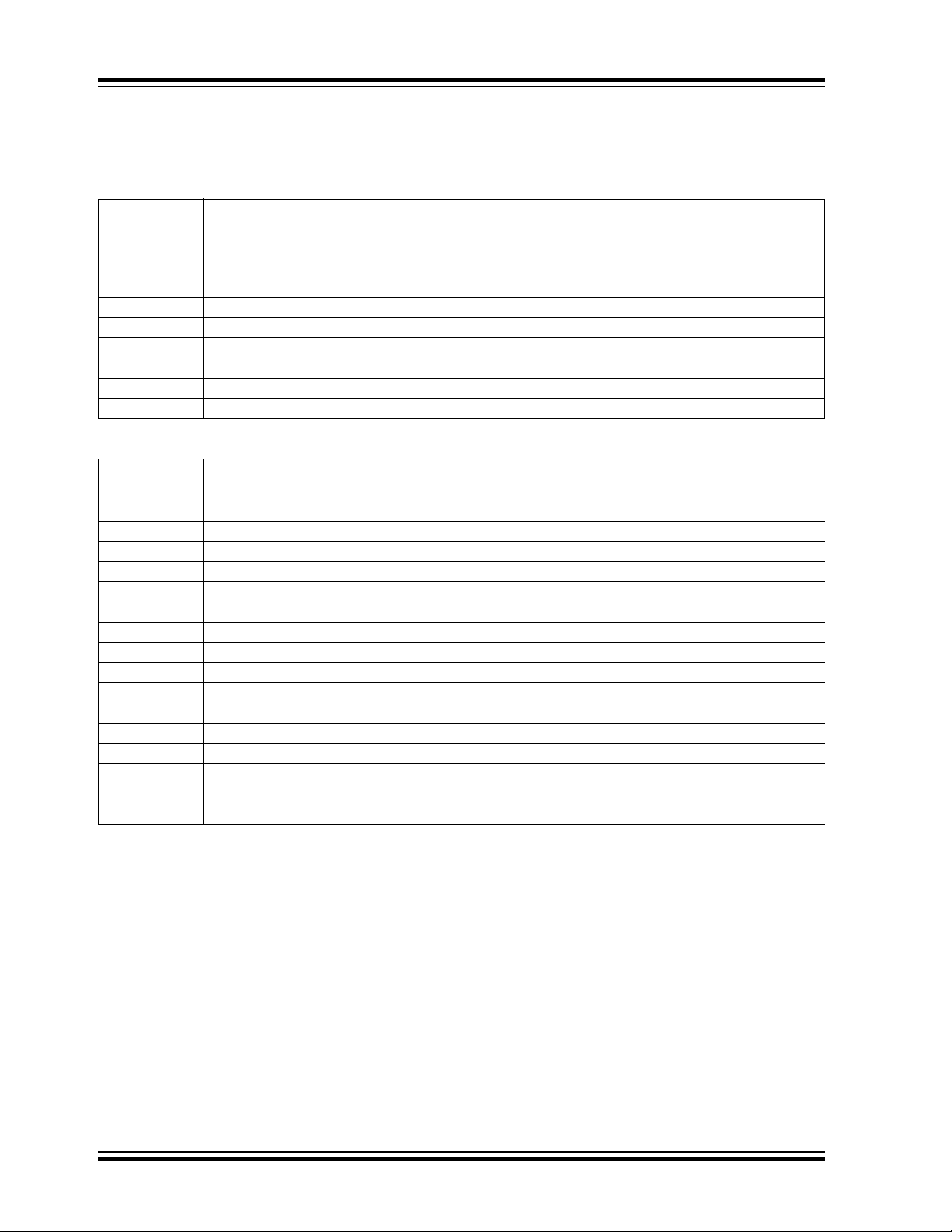
2.0 PIN DESCRIPTIONS
The descriptions of the pins are listed in Table 2-1.
TABLE 2-1: PIN FUNCTION TABLE
Pin No.
(8-Pin DIP)
(8-Pin CERDIP)
1 Zener Cathode Cathode of internal Zener diode.
2C
3 GND Ground terminal.
4C
5V
6 FREQ x 2 If grounded, frequency doubles.
7C
8V
Symbol Description
+
-
OUT
OSC
DD
Positive side of external CP capacitor (pump cap).
Negative side of external CP capacitor (pump cap).
Output voltage.
Capacitor to GND will decrease frequency.
Input voltage.
Pin No.
(16-Pin SOIC)
1 Zener Cathode Cathode of internal Zener diode.
2 NC No connect.
3C
4 NC No connect.
5 GND Ground terminal.
6 NC No connect.
7C
8 NC No connect.
9 NC No connect.
10 V
11 NC No connec t.
12 FREQ x 2 If grounded, frequency doubles.
13 NC No connect.
14 C
15 NC No connect.
16 V
Symbol Description
+
-
OUT
OSC
DD
Positive side of external CP capacitor (pump cap).
Negative side of external CP capacitor (pump cap).
Output voltage.
Capacitor to GND will decrease frequency.
Input voltage.
DS21484D-page 4 2001-2012 Microchip Technology Inc.
Page 5
TC962
TC962
1
2
3
4
8
690
7
5
C
P
+
10 μF
C
OSC
R
L
V
OUT
(–5V)
10 μF
C
R
I
L
I
S
V
(+5V)
+
NC
+
1
2
3
TC962
4
8
7
6
5
C
P2
C
P1
C
R1
10 μF
V
+
+
+
+
10 μF
V
OUT
= –V
+
V
D1
V
D2
V
OUT
=
+
10 μF
Combined Negative Converter and Positive Multiplier
+
C
P
10 μF
+
1
2
3
4
8
7
6
5
10 μF
C
R
+
V
OUT
=
V
2
+
Split V+ In Half
TC962
Positive Voltage MultiplierLowering Output Resistance by Paralleling Devices
2V –2V
D
TC962
1
2
3
4
8
7
6
5
10 μF
10 μF
V
OUT
=
+
V
D2
V
D1
++
V
+
C
P
C
P
2V –2V
D
C
P1
10 μF
+
C
P2
10 μF
+
TC962
TC962
1
2
3
4
8
7
6
5
1
2
3
4
8
7
6
5
+
V
+
V
OUT
10 μF
C
R
V
+
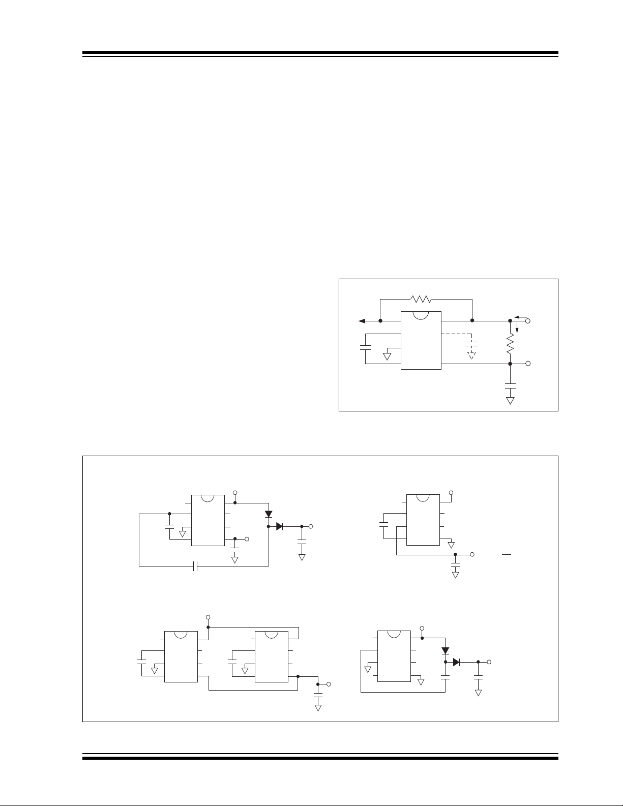
3.0 APPLICATIONS INFORMATION
3.1 Theory of Operation
The TC962 is a capacitive pump (sometimes called a
switched capacitor circuit), where four MOSFET
switches control the charge and discharge of a
capacitor.
The functional block diag ram sho w s how the switc hing
action works. SW1 and SW2 are turned on simultaneously, charging C
assumes that the on resistance of the MOSFETs in
series with the capacitor results in a charging time
(3 time constants) that is less than the on tim e provided
by the oscillator frequency as shown:
3 (R
DS(ON) CP
In the next cycle, SW1 and SW2 are turned off and af ter
a very short interval of all switches being off (this
prevents large currents from occurring due to cross
conduction), SW3 and SW4 are turn ed o n. Th e c harg e
is then transferred to CR, but with the polarity
in C
P
inverted. In this way, a negative voltage is now derived.
An oscillator supplies pulses to a flip-flop that is then
fed to a set of level shifters. These level shifters then
drive each set of switches at one-half the oscillator
frequency.
The oscillator has two pins that control the frequency of
oscillation. Pin 7 can have a capacitor added that is
returned to ground. This w ill lo w er th e freq uen cy of th e
oscillator by adding cap acit ance to th e timing c apa citor
internal to the TC962. Grounding pin 6 will turn on a
to the supply voltage, VIN. This
P
) < CP/(0.5 f
OSC
)
current source and double the frequency. This will
double the charge current going into the internal
capacitor, as well as any capacitor added to pin 7.
A Zener diode has been a dded to the TC962 fo r use as
a reference in building external regulators. This Zener
runs from pin 1 to ground.
3.2 Latch-Up
All CMOS structures contain a parasitic SCR. Care
must be taken to preven t any input from going ab ove or
below the supply rail, or latch-up will occur. The result
of latch-up is an effective short between V
Unless the power supply input has a current limit, this
latch-up phenomena will result in damage to the
device. (See AN763, Latch-up Protection for MOSFET
Drivers.)
FIGURE 3-1: Test Circuit
and VSS.
DD
FIGURE 3-2: Typical Applications
2001-2012 Microchip Technology Inc. DS21484D-page 5
Page 6
TC962
-60 -40 -20 0 20 40 60 80 100 120 140
TEMPERATURE (°C)
80
70
60
50
40
30
20
OUTPUT RESISTANCE ( )
Output Resistance vs. Temperature
10
Ω
50
4.5
ZENER VOLTAGE (V)
CURRENT (mA)
Current vs. Zener Voltage
4.0
5.5 6.0 6.5 7.0
40
30
20
10
0
100
LOAD CURRENT (mA)
POWER CONVERSION EFFICIENCY (%)
Power Conversion Efficiency vs. I
16 32 48 64 80
80
60
40
20
90
70
50
30
10
0
824405672
LOAD
150
120
90
60
30
135
105
75
45
15
0
SUPPLY CURRENT (mA)
V = 5V IL = 3 mA
+
V = 15V IL = 20 mA
+
TA = +25°C
TA = +25°C
EFFICIENCY
SUPPLY
CURRENT
100
INPUT VOLTAGE (V)
OUTPUT RESISTANCE (Ω)
Output Resistance vs. Input Voltage
4 8 12 16 20
80
60
40
20
90
70
50
30
10
2 6 10 14 180
110
TA = +25°C
3 μA
20 μA
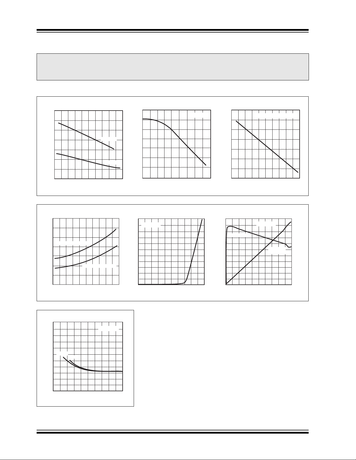
4.0 TYPICAL CHARACTERISTICS
Note: The graphs and tables provided following this note are a statistical summary based on a limit ed n um ber o f
samples and are provided for informational purposes only. The performance characteristics listed herein
are not tested or guaranteed. In some graphs or tables, the data presented may be outside the specified
operating range (e.g., outside specified power supply range) and therefore outside the warranted range.
Circuit of Figure , CP = CR = 10 F, C
PESR
C
RESR
1.
Supply Current vs. Temperature
700
600
500
+
400
300
200
SUPPLY CURRENT (μA)
100
0
-60 -40 -20 0 20 40 60 80 100 120 140
TEMPERATURE (°C)
V = 15V
+
V = 15V
Oscillator Frequency vs. C
10k
1k
100
FREQUENCY (Hz)
10
10 100 1000 10,000
1
CAPACITANCE (pF)
OSC
TA = +25°C
Frequency vs. Temperature
20
18
16
14
12
10
FREQUENCY (kHz)
8
6
-60 -40 -20 0 20 40 60 80 100 120 140
C
= FREQ x 2 = OPEN
OSC
TEMPERATURE (°C)
DS21484D-page 6 2001-2012 Microchip Technology Inc.
Page 7
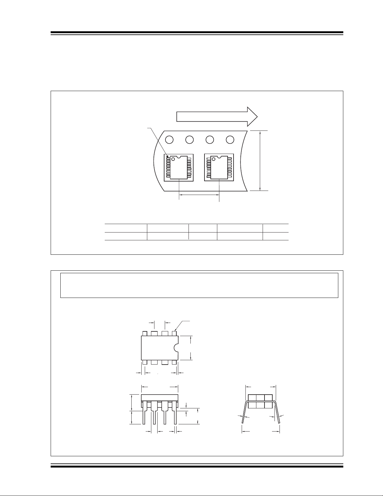
5.0 PACKAGING INFORMATION
Component Taping Orientation for 16-Pin SOIC (Wide) Devices
W
Pin 1
User Direction of Feed
Standard Reel Component Orientation
for 713 Suffix Device
P
Package Carrier Width (W) Pitch (P) Part Per Full Reel Reel Size
16-Pin SOIC (W) 16 mm 12 mm 1000 13 in
Carrier Tape, Number of Components Per Reel and Reel Size
.400 (10.16)
.370 (9.40)
.300 (7.62)
.230 (5.84)
.065 (1.65)
.045 (1.14)
.055 (1.40) Max.
.020 (0.51) Min.
Pin 1
.200 (5.08)
.160 (4.06)
.200 (5.08)
.125 (3.18)
.110 (2.79)
.090 (2.29)
.020 (0.51)
.016 (0.41)
.040 (1.02)
.020 (0.51)
.320 (8.13)
.290 (7.37)
.150 (3.81)
Min.
3° Min.
8-Pin CDIP (Narrow)
.015 (0.38)
.008 (0.20)
.400 (10.16)
.320 (8.13)
Dimensions: inches (mm)
Note: For the most current package drawings, please see the Microchip Packaging Specification located
at http://www.m ic roc hip.c om /p a ckagi ng
5.1 Package Marking Information
Package marking data not available at this time.
5.2 Taping Form
TC962
5.3 Package Dimensions
2001-2012 Microchip Technology Inc. DS21484D-page 7
Page 8
TC962
3° Min.
Pin 1
.260 (6.60)
.240 (6.10)
.045 (1.14)
.030 (0.76)
.070 (1.78)
.040 (1.02)
.400 (10.16)
.348 (8.84)
.200 (5.08)
.140 (3.56)
.150 (3.81)
.115 (2.92)
.110 (2.79)
.090 (2.29)
.022 (0.56)
.015 (0.38)
.040 (1.02)
.020 (0.51)
.015 (0.38)
.008 (0.20)
.310 (7.87)
.290 (7.37)
.400 (10.16)
.310 (7.87)
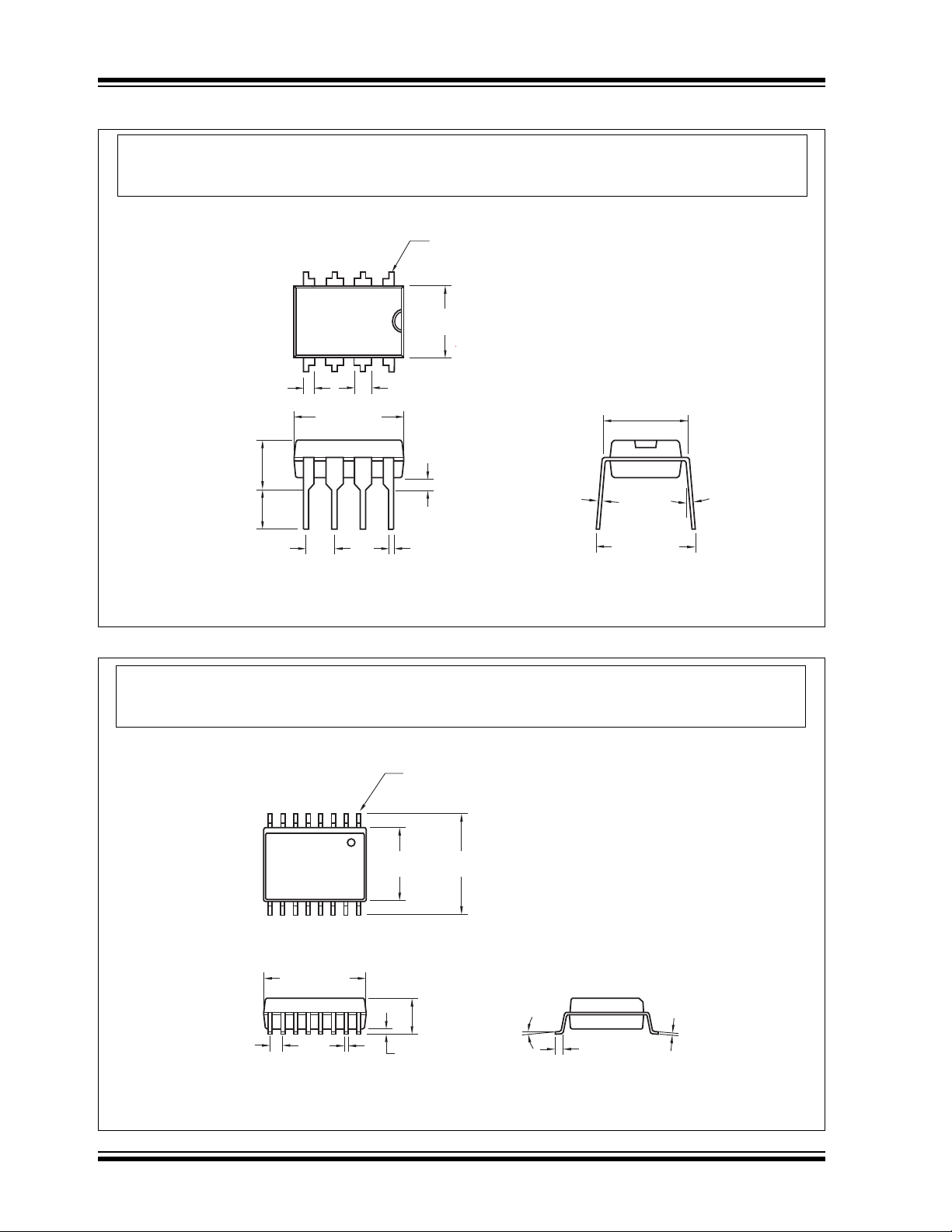
8-Pin Plastic DIP
Dimensions: inches (mm)
Note: For t he mo s t c ur re nt pac ka g e d raw in gs , pl ea se see th e M ic r oc hi p Pa c ka gi n g Specif ic ati on lo c at ed
at http://www.microchip.com/packaging
Note: For the most current package drawings, please see the Microchip Packaging Specification located
at http://www.microchip.com/packaging
Package Dimensions (Continued)
16-Pin SOIC (Wide)
Pin 1
.413 (10.49)
.050 (1.27) Typ.
DS21484D-page 8 2001-2012 Microchip Technology Inc.
.398 (10.10)
.019 (0.48)
.014 (0.36)
.299 (7.59)
.291 (7.40)
.419 (10.65)
.398 (10.10)
.104 (2.64)
.097 (2.46)
.012 (0.30)
.004 (0.10)
8°
Max.
.050 (1.27)
.016 (0.40)
Dimensions: inches (mm)
.013 (0.33)
.009 (0.23)
Page 9

6.0 REVISION HISTORY
Revision D (December 2012)
Added a note to each package outline drawing.
TC962
2001-2012 Microchip Technology Inc. DS21484D-page 9
Page 10

TC962
NOTES:
DS21484D-page 10 2001-2012 Microchip Technology Inc.
Page 11

TC962
THE MICROCHIP WEB SITE
Microchip provides onlin e support v ia our W WW site at
www.microchip.com. This web site is used as a m ean s
to make files and information easily available to
customers. Accessible by using your favorite Internet
browser, the web site contains the following
information:
• Product Support – Data sheets and errata,
application notes and sample programs, design
resources, user’s guides and hardware support
documents, latest software releases and archived
software
• General Technical Support – Frequently Asked
Questions (FAQ), technical support requests,
online discussion groups, Microchip consultant
program member listing
• Business of Microchip – Product selector and
ordering guides, latest Microchip press releases,
listing of s eminars and events, listings of
Microchip sales offices, distributors and factory
representatives
CUSTOMER CHANGE NOTIFICATION
SERVICE
CUSTOMER SUPPORT
Users of Microchip products can receive assistance
through several channels:
• Distributor or Representative
• Local Sales Office
• Field Application Engineer (FAE)
• Technical Support
Customers should contact their distributor,
representative or field application engineer (FAE) for
support. Local sales offices are also av ailable to help
customers. A listing of sales offices and locations is
included in the back of this document.
T echnic al suppo rt is avail able throug h the web si te
at: http://microchip.com/support
Microchip’s customer notification service helps keep
customers current on Microchip products. Subscribers
will receive e-mail notification whenever there are
changes, updates, revisions or errata related to a
specified produ ct family or develo pment tool of inte rest.
To register, access the Microchip web site at
www.microchip.com. Under “Support”, click on
“Customer Change Notification” and follow the
registration instructions.
2001-2012 Microchip Technology Inc. DS21484D-page 11
Page 12

TC962
TO: Technical Publications Manager
RE: Reader Response
Total Pages Sent ________
From:
Name
Company
Address
City / State / ZIP / Country
Telephone: (_______) _________ - _________
Application (optional):
Would you like a reply? Y N
Device: Literature Number:
Questions:
FAX: (______) _________ - _________
DS21484DTC962
READER RESPONSE
It is our intention to provide you with the best documentation possible to ensure successful use of your Microchip
product. If you wish to provide your comments on organization, clarity, subject matter, and ways in which our
documentation can better serve you, please FAX your comments to the Technical Publications Manager at
(480) 792-4150.
Please list the following information, and use this outline to provide us with your comments about this document.
1. What are the best features of this document?
2. How does this document meet your hardware and software development needs?
3. Do you find the organization of this document easy to follow? If not, why?
4. What additions to the document do you think would enhance the structure and subject?
5. What deletions from the document could be made without affecting the overall usefulness?
6. Is there any incorrect or misleading information (what and where)?
7. How would you improve this document?
DS21484D-page 12 2001-2012 Microchip Technology Inc.
Page 13

Note the following details of the code protection feature on Microchip devices:
YSTEM
CERTIFIED BY DNV
== ISO/TS 16949 ==
• Microchip products meet the specification contained in their particular Microchip Data Sheet.
• Microchip believes that its family of products is one of the most secure families of its kind on the market today, when used in the
intended manner and under normal conditions.
• There are dishonest and possibly illegal methods used to breach the code protection feature. All of these methods, to our
knowledge, require using the Microchip products in a manner outside the operating specifications contained in Microchip’s Data
Sheets. Most likely, the person doing so is engaged in theft of intellectual property.
• Microchip is willing to work with the customer who is concerned about the integrity of their code.
• Neither Microchip nor any other semiconductor manufacturer can guarantee the security of their code. Code protection does not
mean that we are guaranteeing the product as “unbreakable.”
Code protection is constantly evolving. We at Microchip are com mitted to continuously improving the c ode prot ection f eatures of our
products. Attempts to break Microchip’s code protection feature may be a violation of t he Digit al Mill ennium Copyright Act. If such act s
allow unauthorized access to your software or other copyrighted work, you may have a right to sue for relief under that Act.
Information contained in this publication regarding device
applications and t he lik e is provided only for your c onvenience
and may be su perseded by updates. It is y our responsibility to
ensure that your application meets with your specifications.
MICROCHIP MAKES NO REPRESENTATIONS OR
WARRANTIES OF ANY KIND WHETHER EXPRESS OR
IMPLIED, WRITTEN OR ORAL, STATUTORY OR
OTHERWISE, RELATED TO THE INFORMATION,
INCLUDING BUT NOT LIMITED TO ITS CONDITION,
QUALITY, PERFORMANCE, MERCHANTABILITY OR
FITNESS FOR PURPOSE. Microchip disclaims all liability
arising from this information and its use. Use of Microchip
devices in life supp ort and/or safety ap plications is entir ely at
the buyer’s risk, and the buyer agrees to defend, indemnify and
hold harmless M icrochip from any and all dama ges, claims,
suits, or expenses re sulting from such use. No licens es are
conveyed, implicitly or otherwise, under any Microchip
intellectual property rights.
Trademarks
The Microchip name and logo, the Microchip logo, dsPIC,
FlashFlex, K
PICSTART, PIC
and UNI/O are registered trademarks of Microchip T echnology
Incorporated in the U.S.A. and other countries.
FilterLab, Hampshire, HI-TECH C, Linear Active Thermistor,
MTP, SEEVAL and The Embedded Control Solutions
Company are registered trademarks of Microchip Technology
Incorporated in the U.S.A.
Silicon Storage Technology is a registered trademark of
Microchip Technology I nc. in other countries.
Analog-for-the-Digital Age, Application Maestro, BodyCom,
chipKIT, chipKIT logo, CodeGuard, dsPICDEM ,
dsPICDEM.net, dsPICworks, dsSPEAK, ECAN,
ECONOMONITOR, FanSense, HI-TIDE, In-Circuit Serial
Programming, ICSP, Mindi, MiWi, MPASM, MPF, MPLAB
Certified logo, MPLIB, MPLINK, mTouch, Omniscient Code
Generation, PICC, PICC-18, PICDEM, PICDEM.net, PICkit,
PICtail, REAL ICE, rfLAB, Select Mode, SQI, Serial Quad I/O,
Total Endurance, TSHARC, UniWinDriver, WiperLock, ZENA
and Z-Scale are trademarks of Microchip Technology
Incorporated in the U.S.A. and other countries.
SQTP is a service mark of Microchip T echnology Incorporated
in the U.S.A.
GestIC and ULPP are registered trademarks of Microchip
Technolo gy Germ any II GmbH & Co . & KG, a subsidiary of
Microchip T echnology Inc., in other countries.
All other trademarks mentioned herein are property of their
respective companies.
© 2001-2012, Microchip Technology Incorporated, Printed in
the U.S.A., All Rights Reserved.
Printed on recycled paper.
ISBN: 9781620768808
EELOQ, KEELOQ logo, MPLAB, PIC, PICmicro,
32
logo, rfPIC, SST, SS T Logo, SuperFlash
QUALITY MANAGEMENT S
2001-2012 Microchip Technology Inc. DS21484D-page 13
Microchip received ISO/TS-16949:2009 certification for its worldwide
headquarters, design and wafer fabrication facilities in Chandler and
Tempe, Arizona; Gresham, Oregon and design centers in California
and India. The Company’s quality system processes and procedures
are for its PIC
devices, Serial EEPROMs, microperipherals, nonvolatile memory and
analog products. In addition, Microchip’s quality system for the design
and manufacture of development systems is ISO 9001:2000 certified.
®
MCUs and dsPIC® DSCs, KEELOQ
®
code hopping
Page 14

Worldwide Sales and Service
AMERICAS
Corporate Office
2355 West Chandler Blvd.
Chandler, AZ 85224-6199
Tel: 480-792-7200
Fax: 480-792-7277
Techn ical Su pport:
http://www.microchip.com/
support
Web Address:
www.microchip.com
Atlanta
Duluth, GA
Tel: 678-957-9614
Fax: 678-957-1455
Boston
Westborough, MA
Tel: 774-760-0087
Fax: 774-760-0088
Chicago
Itasca, IL
Tel: 630-285-0071
Fax: 630-285-0075
Cleveland
Independence, OH
Tel: 216-447-0464
Fax: 216-447-0643
Dallas
Addison, TX
Tel: 972-818-7423
Fax: 972-818-2924
Detroit
Farmington Hills, MI
Tel: 248-538-2250
Fax: 248-538-2260
Indianapolis
Noblesville, IN
Tel: 317-773-8323
Fax: 317-773-5453
Los Angeles
Mission Viejo, CA
Tel: 949-462-9523
Fax: 949-462-9608
Santa Clara
Santa Clara, CA
Tel: 408-961-6444
Fax: 408-961-6445
Toronto
Mississauga, Ontario,
Canada
Tel: 905-673-0699
Fax: 905-673-6509
ASIA/PACIFIC
Asia Pacific Office
Suites 3707-14, 37th Floor
Tower 6, The Gateway
Harbour City, Kowloon
Hong Kong
Tel: 852-2401-1200
Fax: 852-2401-3431
Australia - Sydney
Tel: 61-2-9868-67 33
Fax: 61-2-9868-6755
China - Beijing
Tel: 86-10-8569-7 000
Fax: 86-10-8528-2104
China - Chengdu
Tel: 86-28-8665-5 511
Fax: 86-28-8665-7889
China - Chongqing
Tel: 86-23-8980-9 588
Fax: 86-23-8980-9500
China - Hangzhou
Tel: 86-571-2819- 3187
Fax: 86-571-2819-3189
China - Hong Kong SAR
Tel: 852-2943-5100
Fax: 852-2401-3431
China - Nanjing
Tel: 86-25-8473-2 460
Fax: 86-25-8473-2470
China - Qingdao
Tel: 86-532-8502- 7355
Fax: 86-532-8502-7205
China - Shanghai
Tel: 86-21-5407-5 533
Fax: 86-21-5407-5066
China - Shenyang
Tel: 86-24-2334-2 829
Fax: 86-24-2334-2393
China - Shenzhen
Tel: 86-755-8864- 2200
Fax: 86-755-8203-1760
China - Wuhan
Tel: 86-27-5980-5 300
Fax: 86-27-5980-5118
China - Xian
Tel: 86-29-8833-7 252
Fax: 86-29-8833-7256
China - Xiamen
Tel: 86-592-2388138
Fax: 86-592-2388130
China - Zhuhai
Tel: 86-756-3210040
Fax: 86-756-3210049
ASIA/PACIFIC
India - Bangalore
Tel: 91-80-3090-4444
Fax: 91-80-3090-4123
India - New Delhi
Tel: 91-11-4160-8631
Fax: 91-11-4160-8632
India - Pune
Tel: 91-20-2566-1512
Fax: 91-20-2566-1513
Japan - Osaka
Tel: 81-6-6152-7160
Fax: 81-6-6152-9310
Japan - Tokyo
Tel: 81-3-6880- 3770
Fax: 81-3-6880-3771
Korea - Daegu
Tel: 82-53-744-4301
Fax: 82-53-744-4302
Korea - Seoul
Tel: 82-2-554-7200
Fax: 82-2-558-5932 or
82-2-558-5934
Malaysia - Kuala Lumpur
Tel: 60-3-6201-9857
Fax: 60-3-6201-9859
Malaysia - Penang
Tel: 60-4-227-8870
Fax: 60-4-227-4068
Philippines - Manila
Tel: 63-2-634-9065
Fax: 63-2-634-9069
Singapore
Tel: 65-6334-8870
Fax: 65-6334-8850
Tai wan - Hsin Chu
Tel: 886-3-5778-366
Fax: 886-3-5770-955
Taiwan - Kaohsiung
Tel: 886-7-213-7828
Fax: 886-7-330-9305
Taiwan - Taipei
Tel: 886-2-2508-8600
Fax: 886-2-2508-0102
Thailand - Bangkok
Tel: 66-2-694-1351
Fax: 66-2-694-1350
EUROPE
Austria - Wels
Tel: 43-7242-2244-39
Fax: 43-7242-2244-393
Denmark - Copenhagen
Tel: 45-4450-2828
Fax: 45-4485-2829
France - Paris
Tel: 33-1-69-53 -63-20
Fax: 33-1-69-30-90-79
Germany - Munich
Tel: 49-89-627- 144-0
Fax: 49-89-627-144-44
Italy - Milan
Tel: 39-0331-742611
Fax: 39-0331-466781
Netherlands - Drunen
Tel: 31-416-690399
Fax: 31-416-690340
Spain - Madrid
Tel: 34-91-708- 08-90
Fax: 34-91-708-08-91
UK - Wokingham
Tel: 44-118-921-5869
Fax: 44-118-921-5820
11/29/12
DS21484D-page 14 2001-2012 Microchip Technology Inc.
 Loading...