

Page 1

TC9208M
Preliminary Dat
8
-
P
o
r
t
10/100/1000 S
m
a
r
t
E
t
h
e
r
n
e
t
S
w
i
t
c
h
a
Sheet
Features
Stand Alone Switch On A Chip
8 Ethernet 10/100/1000 ports
MII/GMII interface for all ports
Trunk group support
s of Service (CoS) sele
Four Cl
each port and/or checked via IP Header and
802.1Q VLAN Tag
Eight port-based VLANs
Maximum throughp
blocking architecture
Em
8K MAC address table
Each
100 full/half duplex and 1000 full duplex mode
Flow-control ability is able to set for both full
and half duplex mode
Broadcast throttling
Port Mirroring
S
MDIO master for PHY configuration / polling
0.18 micron technology
2V and 3.3V dual voltage power supply
Packaged in PBGA 292
27 MHz crystal input only
asse
ut, non hea
bedded SSRAM packet
configurable to
s
port i
rial EEPROM Interface, EEPROM is optional
e
ctab
d-o
buffer/address
10 full/half d
le for
-line
f
table
uplex,
General Description
,
whi
00
c
h
rt 10/100/10
a
cket buf
fer
s for each
.
ted 8 po
be
ds p
a fully integra
08M is
TC92
smart Ethernet switch controller designed for low
cost and high performance solutions. The chip
embeds necessary SSRAM for packet buffering
and MAC address table. It provides MII / GMII
interface for all port
A store-and-forward switching method using a
non-blocking architecture is implemented within
TC9208M to improve the availability and
band
wi
d
t
h. The chip em
s no
it suppo
transmission port.
TC9208M provides evolved CoS with four levels
of priority. The priority can be checked via layer 2
(802.1Q VLAN Tagging) and/or layer 3 (IP Header
TOS bits) packets. Port based priority is also
provided to ensure transmission with precedence
for all packets incoming from selected port(s).
rt
s
rmal and priority queue
This feature allows improved support for
c to im
8K add
an
earnin
nfig
ram
plement flow
ss-loo
re
, and a
g
cellent add
x
nterface
uration i
configuration
s
ng. A virtua
mi
terface in the
s for
control for
rol for full
table
kup
tic agi
a
tom
u
ress sp
compri
ses 40
n
terface, the
l internal
abse
ng,
ace
n
ce
multimedia applications.
s IEEE 802.3 MAC function
cessa
handle
n
chi
r
nfiguration i
c
e to
bed
y logi
r
s
g, self-l
ed and e
spe
pin co
rog
mming in
The chip em
each port and these functions support full and half
duplex modes for both 10 and 100 Mbits/s data
rates and full duplex for 1000 Mbit/s. Each port
includes dedicated receive and transmit FIFOs
with ne
both full and half duplex modes. TC9208M uses
IEEE 802.3x frame based flow cont
duplex and backpressure for half duplex.
08M
TC92
with sea
at very high
coverage. Forwarding rules are implemented
according to IEEE 802.1D specifications. Filtering
capabilities for bad packets and packets with
Reserved Group Address DA are also provided.
Increased interconnection bandwidth can be
achieved by using TC9208M’s trunking
capabilities. Several load-balancing schemes are
provided through pin and EEPROM configuration.
A port mirror feature, which it includes bad frames
optionally, can be used for debugging network
problems.
The pin co
configurations, which are shared with GMII output
pins by latching the configuration data during
reset. An external EEPROM device can also be
used to configure the TC9208M at power-up. With
referen
EEPROM extends the chip’
capability with new features and enables a
jumper-less configuration mode using a parallel
interface for rep
EEPROM mode is also provided to enable the
use of the progra
of external EEPROM. TC9208M can make
effective use by most of its features using only the
pin configuration interface.
TC9208M includes a physical layer configuration /
polling entity, which it is use to configure the phy
functions and to monitor the physical layer
transceiver’s speed, duplex mode, link status and
full duplex flow control ability for each port. The
chip provides four modes for phy configurations,
Confidential.
Copyright © 2003, IC Plus Corp. TC9208M-DS-R06
1/53
August 1, 2003
Page 2
which these modes include auto-negotiation
disable procedure for 10/100 speed modes. The
phy configuration information is stored in
EEPROM setting.
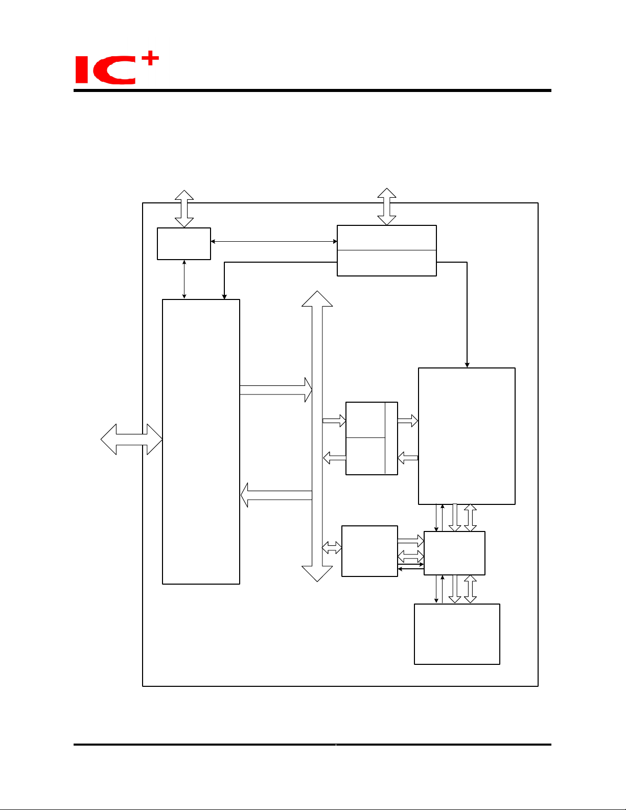
Block Diagram
TC9208M
Preliminary Data Sheet
The chip requires 27 MHz system clock, dual 2V
and 3.3V power supply and is packaged in PBGA
292.
External PHY's
MDIO
interface
8 GM II/MII
RX/TX MAC's
Fro m RX MAC
To TX MA C
EEprom Interface
Configuration
Register
Rx FIFO
Control
Tx FIFO
Address
LoockUp
&
Reso lution
Unit
Queue
Management
Memory
Inte rface
&
Arbiter
Inte rna l
TC9208M
SSRAM
Buffer
Block Diagram
Confidential.
Copyright © 2003, IC Plus Corp. TC9208M-DS-R06
2/53
August 1, 2003
Page 3

TC9208M
Preliminary Data Sheet
Table Of Contents
Features ..............................................................................................................................................................1
General Description ............................................................................................................................................ 1
Block Diagram.....................................................................................................................................................2
Table Of Contents...............................................................................................................................................3
Revision History .................................................................................................................................................. 4
Pins Placement...................................................................................................................................................5
Pin Listing (PBGA 292)...............................................................................................................................6
1
2 Ethernet Media Access Controller ............................................................................................................17
2.1 Receive MAC .....................................................................................................................17
2.2
Transmit MAC ....................................................................................................................18
3 MAC Address Handling.............................................................................................................................19
4 Queue Management.................................................................................................................................19
5
Classes of Service ....................................................................................................................................20
Trunk Configuration...................................................................................................................................22
6
7
Flow Control ..............................................................................................................................................22
8 Broadcast Throttling ..................................................................................................................................24
9 Port Mirroring.............................................................................................................................................24
10 Physical Layer Configuration / Polling......................................................................................................25
11 EEPROM Interface ...................................................................................................................................26
11.1 Reprogramming the EEPROM for reconfiguration ............................................................ 26
11.2 EEPROM Address Map ..................................................................................................... 27
11.3 Register Description........................................................................................................... 29
11.3.1 Validation Register ................................................................................................ 29
11.3.2 Port [X] Configuration Register ............................................................................. 31
11.3.3 Port [X] IFG Configuration Register ...................................................................... 33
11.3.4 Flow Control Register ........................................................................................... 34
11.3.5 Backpressure Time Value Register....................................................................... 35
11.3.6 Flow Control Port Base Address Register ............................................................ 36
11.3.7 Trunk Configuration Register................................................................................ 36
11.3.8 Broadcast Configuration Register......................................................................... 37
11.3.9 IP Priority Mapping Register ................................................................................. 38
11.3.10 VLAN Priority Mapping Register ........................................................................... 39
11.3.11
11.3.12
11.3.13
11.3.14
11.3.15
11.3.16
11.3.17
11.4 Writing / Reading PHY management registers via EEPROM interface............................. 46
11.4.1 Data Write Register............................................................................................... 46
11.4.2
11.4.3 Physical Layer’s Register Address Register ......................................................... 47
11.4.4 IO Status Control Register.................................................................................... 47
11.4.5
12 Timing Requirements................................................................................................................................49
12.1 GMII / MII Receive Timing Requirements.......................................................................... 49
12.2
GMII / MII Transmit Timing................................................................................................. 49
12.3 PHY Management (MDIO) Timing ..................................................................................... 50
12.4 EEPROM Timing................................................................................................................ 51
13
Electrical Specifications ............................................................................................................................52
CoS Bandwidth Register....................................................................................... 40
Reserved Register ................................................................................................ 40
CoS Configuration Register .................................................................................. 41
Port Mirroring Register.......................................................................................... 42
General Configuration Register ............................................................................ 43
Port VLAN Enable Register .................................................................................. 44
VLAN [Y] Register................................................................................................. 45
Physical Layer Device Address Register .............................................................. 46
Data Read Register .............................................................................................. 48
Confidential.
Copyright © 2003, IC Plus Corp. TC9208M-DS-R06
3/53
August 1, 2003
Page 4

TC9208M
Preliminary Data Sheet
13.1
ABSOLUTE MAXIMUM RATINGS..................................................................................... 52
13.2
RECOMMENDED OPERATING CONDITIONS ................................................................ 52
13.3 DC CHARACTERISTICS................................................................................................... 52
Package Detail ..........................................................................................................................................53
14
Revision History
Revision # Change Description
TC9208-DS-R05
TC9208-DS-R06 1. Modify The “Pin Latched” field in Class of Service section and the “Pin Latched”
field in Trunk Configuration.
2. Correct the register map of “Broadcast Configuration Register”
3. Correct the junction temperature limit.
Confidential.
Copyright © 2003, IC Plus Corp. TC9208M-DS-R06
4/53
August 1, 2003
Page 5

Pins Placement
TC9208M
Preliminary Data Sheet
1234
RXD00 CRS0 COL0 TXD76 TXD73 TXD70 RXDV7 RXER7 RXD74 RXD73 RXD70 TXER6 TXD66 TXD63 TXD60 RXER6 RXD65 RXD64 RXD63 RXD62
A
RXD03 RXD02 RXD01 TXD77 TXD74 TXD71 RXD75 RX D72 CRS7 TXEN6 TXD65 TXD62 RXD66 RXD61 RXD60 CRS6
B
RXD06 RXD05 RXD04 TXER7 TXD75 TXD72 RXD77 RXD76 RXD71 COL7 TXD67 TXD64 TXD61 RXDV6 RXD67 COL6 SDA
C
RXDV0 RXD07 RXER0 T XEN7 VSS2.0 VDD3.3 VDD2.0 VSS2.0 VSS3.3 VSS3.3 VSS2.0 V DD2.0 VDD3.3 VSS3.3 VSS3.3 VSS2.0 SCL MDIO MDC
D
TXD00 VSS3.3 TXER5 TXEN5 TXD57 TXD56
E
TXD03 TXD02 TXD01 VSS3.3 VSS2.0 TXD55 TXD54 TXD53
F
TXD06 TXD05 TXD04 VDD3.3 VDD3.3 TXD50 TXD51 TXD52
G
TXER0 TXEN0 TXD07 VDD2.0 VDD2.0 RXER5 RXDV5
H
RXD10 CRS1 COL1 VDD3.3 RXD57 RXD56
J
RXD13 RXD12 RXD11 VSS2.0 VDD3.3 RXD55 RXD54 RXD53
K
RXD17 RXD16 RXD15 RXD14 VSS3.3 RXD52 RXD51 RXD50
L
RXDV1 VDD3.3 VDD3.3 TXEN4 COL5 CRS5
M
RXER1 TXD10 VDD2.0 VDD2.0 TXD46 TXD47 TXER4
N
RXCLK0
GTXCLK0TXCLK0
GTXCLK1RXCLK1
TXCLK1
5
7891011
6
RXCLK7
GTXCLK7
TXCLK7
GND GND GND GND GND GND
GND GND GND GND GND GND
GND GND GND GND GND GND
GND GND GND GND GND GND
GND GND GND GND GND GND
GND GND GND GND GND GND
12
13
14 15 16 17 18 19
RXCLK6TXCLK6
GTXCLK6
TXCLK5
GTXCLK5RXCLK5
TESTINT
20
A
B
C
D
E
F
G
H
J
K
L
M
N
TXD11 TXD12 TXD13 VDD3.3 VDD3.3 TXD43 TXD44 TXD45
P
TXD16 TXD15 TXD14 VSS3.3 VSS2.0 TXD40 TXD41 TXD42
R
TXD17 TXER1 TXEN1 VSS2.0 RXDV4
T
SELSCK
GTXCK RESET
U
VDD18PLL
V
CRS2 RXD20 COL2 RXD25 RXDV2 TXD21 TXD24 TXD27 CRS3 RXD31 RXD34 RXD37 TXD30 TXD33 TXD36 TXEN3 RXD40 RXD43
W
RXD21 RXD22 RXD23 RXD26 RXER2 TXD20 TXD25 TXD26 TXER2 RXD32 RXD33 RXDV3 RXER3 TXD34 TXD37 T XER3 RXD41 RXD42
Y
SYSCK VSS3.3 VSS3.3 VDD3.3 VDD2.0 VDD3.3 VSS3.3 VSS3.3 VDD3.3 VDD2.0 VDD3.3 VSS3.3 VSS2.0 RXD45 RXD46 RXD47 RXER4
D
D
E
E
L
L
T
S
C
B
RXD24 RX D27 TXD22 TXD23 T XEN2 COL3 RXD30 RXD35 RXD36 TXD31 TXD32 TXD35 COL4 CRS4 RXD44
N
U
V
O
RXCLK2
TXCLK2
RXCLK3
TXCLK3GTXCLK2
GTXCLK3
RXCLK4
12345678910111213141516171819
Top View
GTXCLK4
TXCLK4
20
P
R
T
U
V
W
Y
Confidential.
5/53
August 1, 2003
Copyright © 2003, IC Plus Corp. TC9208M-DS-R06
Page 6

1 Pin Listing (PBGA 292)
TC9208M
Preliminary Data Sheet
I ⇒ digital input
I
⇒ schmitt trigger digital input
s
⇒ digital input with internal pull down
I
pd
I/O ⇒ digital bi-directional
⇒ digital bi-directional with internal pull up
I/O
pu
O ⇒ digital output
P ⇒ power
G ⇒ ground
I/Opd ⇒ digital bi-directional with internal pull down
No. Pin label Typ e Description
G4 Vdd 3.3 P Digital +3.3V power supply for I/O
C12 TxData6_7 O GMII transmit data - bits 7
A13 TxData6_6 O GMII transmit data - bits 6
B13 TxData6_5 O GMII transmit data - bits 5
E4 Vss 3.3 G Digital ground for I/O
C13 TxData6_4 O GMII transmit data - bits 4
A14 TxData6_3 O GMII/MII transmit data - bits 3
B14 TxData6_2 O GMII/MII transmit data - bits 2
J4 Vdd 3.3 P Digital +3.3V power supply for I/O
TxData6_1 GMII/MII transmit data - bit 1 C14
PriClass6_1
TxData6_0 GMII/MII transmit data - least significant bit A15
Priclass6_0
I/Opd
Priority class - most significant bit.
I/Opu
Priority class - least significant bit. Sets priority level per port basis.
PriClass[6] - '00' - port 6 low priority
PriClass[6] - '01' - port 6 has normal priority
PriClass[6] - '10' - port 6 has high priority
PriClass[6] - '11' - port 6 has very high priority
PriClass[6] is latched on reset
B12 TxEn6 O GMII/MII transmit enable
C15 GTxClk6 O GMII transmit clock
F4 Vss 3.3 G Digital ground for I/O
A12 TxEr6 TxEr6 I/Opd Transmit Error
B15 TxClk6 I MII transmit clock
B20 Crs6 Is MII carrier sense indication
C18 Col6 Is MII collision indication
A16 RxEr6 Is Receive Error
H4 Vdd 2.0 P Digital +2.0V power supply for core
B16 RxClk6 I MII receive clock
C16 RxDv6 Is GMII/MII data valid
B19 RxData6_0 Is GMII receive data - least significant nibble.
MII receive data
B18 RxData6_1 Is GMII receive data - least significant nibble.
MII receive data
A20 RxData6_2 Is GMII receive data - least significant nibble.
MII receive data
K4 Vss 2.0 G Digital ground for core
A19 RxData6_3 Is GMII receive data - least significant nibble.
MII receive data
Confidential.
Copyright © 2003, IC Plus Corp. TC9208M-DS-R06
6/53
August 1, 2003
Page 7

Pin Listing (continued)
No. Pin label Typ e Description
A18 RxData6_4 Is GMII receive data - most significant nibble
A17 RxData6_5 Is GMII receive data - most significant nibble
B17 RxData6_6 Is GMII receive data - most significant nibble
C17 RxData6_7 Is GMII receive data - most significant nibble
M4 Vdd 3.3 P Digital +3.3V power supply for I/O
R4 Vss 3.3 G Digital ground for I/O
B4 TxData7_7 O GMII transmit data – bits 7
A4 TxData7_6 O GMII transmit data – bits 6
C5 TxData7_5 O GMII transmit data – bits 5
N4 Vdd 2.0 P Digital +2.0V power supply for core
B5 TxData7_4 O GMII transmit data – bits 4
A5 TxData7_3 O GMII/MII transmit data - bits 3
C6 TxData7_2 O GMII/MII transmit data - bits 2
T4 Vss 2.0 G Digital ground for core
TxData7_1 GMII/MII transmit data - bit 1 B6
PriClass7_1
TxData7_0 GMII/MII transmit data - least significant bit A6
PriClass7_0
D5 TxEn7 O GMII/MII transmit enable
B7 GTxClk7 O GMII transmit clock
P4 Vdd 3.3 P Digital +3.3V power supply for I/O
C4 TxEr7 I/Opd Transmit Error
C7 TxClk7 I MII transmit clock
B11 Crs7 Is MII carrier sense indication
C11 Col7 Is MII collision indication
A8 RxEr7 Is Receiver Error
U5 Vss 3.3 G Digital ground for I/O
B8 RxClk7 I MII receive clock
A7 RxDv7 Is GMII/MII data valid
A11 RxData7_0 Is GMII receive data - least significant nibble.
C10 RxData7_1 Is GMII receive data - least significant nibble.
B10 RxData7_2 Is GMII receive data - least significant nibble.
U7 Vdd 3.3 P Digital +3.3V power supply for I/O
A10 RxData7_3 Is GMII receive data - least significant nibble.
A9 RxData7_4 Is GMII receive data - most significant nibble
I/Opd
Priority class - most significant bit.
I/Opu
Priority class - least significant bit. Sets priority level per port basis.
PriClass[7] - '00' - port 7 low priority
PriClass[7] - '01' - port 7 has normal priority
PriClass[7] - '10' - port 7 has high priority
PriClass[7] - '11' - port 7 has very high priority
PriClass[7] is latched on reset
MII receive data
MII receive data
MII receive data
MII receive data
TC9208M
Preliminary Data Sheet
Confidential.
Copyright © 2003, IC Plus Corp. TC9208M-DS-R06
7/53
August 1, 2003
Page 8

Pin Listing (continued)
No. Pin label Typ e Description
B9 RxData7_5 Is GMII receive data - most significant nibble
C9 RxData7_6 Is GMII receive data - most significant nibble
C8 RxData7_7 Is GMII receive data - most significant nibble
U6 Vss 3.3 G Digital ground for I/O
U9 Vdd 3.3 P Digital +3.3V power supply for I/O
H3 TxData0_7 O GMII transmit data - bits 7
G1 TxData0_6 O GMII transmit data - bits 6
G2 TxData0_5 O GMII transmit data - bits 5
U10 Vss 3.3 G Digital ground for I/O
G3 TxData0_4 O GMII transmit data - bits 4
F1 TxData0_3 O GMII/MII transmit data - bits 3
F2 TxData0_2 O GMII/MII transmit data - bits 2
U12 Vdd 3.3 P Digital +3.3V power supply for I/O
TxData0_1 GMII/MII transmit data - bit 1 F3
PriClass0_1
TxData0_0 GMII/MII transmit data - least significant bit E1
PriClass0_0
H2 TxEn0 O GMII/MII transmit enable
E3 GTxClk0 O GMII transmit clock
U11 Vss 3.3 G Digital ground for I/O
H1 TxEr0 I/Opd Transmit Error
E2 TxClk0 I MII transmit clock
A2 Crs0 Is MII carrier sense indication
A3 Col0 Is MII collision indication
D4 RxEr0 Is Receive Error
U8 Vdd 2.0 P Digital +2.0V power supply for core
D3 RxClk0 I MII receive clock
D1 RxDv0 Is GMII/MII data valid
A1 RxData0_0 Is GMII receive data - least significant nibble.
B3 RxData0_1 Is GMII receive data - least significant nibble.
B2 RxData0_2 Is GMII receive data - least significant nibble.
U16 Vss 2.0 G Digital ground for core
B1 RxData0_3 Is GMII receive data - least significant nibble.
C3 RxData0_4 Is GMII receive data - most significant nibble
I/Opd
Priority class - most significant bit.
I/Opu
Priority class - least significant bit. Sets priority level per port basis.
PriClass[0] - '00' - port 0 has low priority
PriClass[0] - '01' - port 0 has normal priority
PriClass[0] - '10' - port 0 has high priority
PriClass[0] - '11' - port 0 has very high priority
PriClass[0] is latched on reset
MII receive data
MII receive data
MII receive data
MII receive data
TC9208M
Preliminary Data Sheet
Confidential.
Copyright © 2003, IC Plus Corp. TC9208M-DS-R06
8/53
August 1, 2003
Page 9

Pin Listing (continued)
No. Pin label Typ e Description
C2 RxData0_5 Is GMII receive data - most significant nibble
C1 RxData0_6 Is GMII receive data - most significant nibble
D2 RxData0_7 Is GMII receive data - most significant nibble
U14 Vdd 3.3 P Digital +3.3V power supply for I/O
U15 Vss 3.3 G Digital ground for I/O
T1 TxData1_7 O GMII transmit data - bits 7
R1 TxData1_6 O GMII transmit data - bits 6
R2 TxData1_5 O GMII transmit data - bits 5
U13 Vdd 2.0 P Digital +2.0V power supply for core
R3 TxData1_4 O GMII transmit data - bits 4
P3 TxData1_3 O GMII/MII transmit data - bits 3
P2 TxData1_2 O GMII/MII transmit data - bits 2
R17 Vss 2.0 G Digital ground for core
TxData1_1 GMII/MII transmit data - bit 1 P1
Priclass1_1
TxData1_0 GMII/MII transmit data - least significant bit N3
PriClass1_0
T3 TxEn1 O GMII/MII transmit enable
M3 GTxClk1 O GMII transmit clock
P17 Vdd 3.3 P Digital +3.3V power supply for I/O
T2 TxEr1 I/Opd Transmit Error
N2 TxClk1 I MII transmit clock
J2 Crs1 Is MII carrier sense indication
J3 Col1 Is MII collision indication
N1 RxEr1 Is Receive Error
L17 Vss 3.3 G Digital ground for I/O
M2 RxClk1 I MII receive clock
M1 RxDv1 Is GMII/MII data valid
J1 RxData1_0 Is GMII receive data - least significant nibble.
K3 RxData1_1 Is GMII receive data - least significant nibble.
K2 RxData1_2 Is GMII receive data - least significant nibble.
M17 Vdd 3.3 P Digital +3.3V power supply for I/O
K1 RxData1_3 Is GMII receive data - least significant nibble.
I/Opd
Priority class - most significant bit.
PriClass[1] is latched on reset
I/Opu
Priority class - least significant bit. Sets priority level per port basis.
PriClass[1] - '00' - port 1 low priority
PriClass[1] - '01' - port 1 has normal priority
PriClass[1] - '10' - port 1 has high priority
PriClass[1] - '11' - port 1 has very high priority
PriClass[1] is latched on reset
MII receive data
MII receive data
MII receive data
MII receive data
TC9208M
Preliminary Data Sheet
Confidential.
Copyright © 2003, IC Plus Corp. TC9208M-DS-R06
9/53
August 1, 2003
Page 10

TC9208M
Preliminary Data Sheet
Pin Listing (continued)
No. Pin label Typ e Description
L4 RxData1_4 Is GMII receive data - most significant nibble
L3 RxData1_5 Is GMII receive data - most significant nibble
L2 RxData1_6 Is GMII receive data - most significant nibble
L1 RxData1_7 Is GMII receive data - most significant nibble
U4 selsck Is Selects the source for the system clock.
selsck - ‘1’ - sysck is driven by a 27Mhz external clock.
U1 Gtxck I The 125Mhz reference clock for 1000Mbps operating mode. This
clock is used as a reference clock for the GMII transmission clock for
every port.
V1 Vdd 2.0 P Digital +2.0V power supply for core
V2 BcstLED I/Opd The led can signal filtering of broadcast frames Also the led remains
lit if the POST test fails, which indicates a faulty chip.
V3 OvUnLED O The led is lit whenever a unicast packets overflow condition is reached
and some frames are dropped by the buffer management engine.
D9 Vss 2.0 G Digital ground for core
U3 sysck I The 27Mhz system clock.
U2 reset I
TxData2_7 GMII transmit data - most significant bit W9
TrunkA
Y9 TxData2_6 I/Opd GMII transmit data - bit 6
TxData2_5 GMII transmit data - bit 5 Y8
TnkMod1
TxData2_4 GMII transmit data - bit 4 W8
TnkMod0
TxData2_3 GMII/MII transmit data - bit 3 V8
PriBndw1
N17 Vdd 2.0 P Digital +2.0V power supply for core
General reset.
pus
I/Opd
Trunk channel A configuration pin.
TrunkA - '0' - trunk channel A disabled
TrunkA - '1' - trunk channel A enabled
Trunk channel A is comprised from ports 0 and 1.
TrunkA is latched on reset
I/Opd
Trunk Balance Mode Select
TnkMod(1) is latched on reset
I/Opd
Trunk Balance Mode Select
TnkMod - '00' - Only the source port is used to select the transmission
TnkMod(0) is latched on reset
I/Opd
Priority bandwidth configuration pins.
PriBndw(1)is latched on reset
port inside the trunk.
- '01' -Transmission port is selected using the source address.
- '10' -Transmission port is selected using the source and
destination addresses
- '11'- not used
Confidential.
Copyright © 2003, IC Plus Corp. TC9208M-DS-R06
10/53
August 1, 2003
Page 11

Pin Listing (continued)
No. Pin label Typ e Description
TxData2_2 GMII/MII transmit data - bit 2 V7
PriBndw0
TxData2_1 GMII/MII transmit data - bit 1
W7
PriClass2_1
TxData2_0 GMII/MII transmit data - least significant bit Y7
PriClass0_0
V9 TxEn2 O GMII/MII transmit enable
W6 GTxClk2 O GMII transmit clock
F17 Vss 2.0 G Digital ground for core
Y10 TxEr2 I/Opd Transmit Error
Y6 TxClk2 I MII transmit clock
W1 Crs2 Is MII carrier sense indication
W3 Col2 Is MII collision indication
Y5 RxEr2 Is Receive Error
K17 Vdd 3.3 P Digital +3.3V power supply for I/O
V6 RxClk2 I MII receive clock
W5 RxDv2 Is GMII/MII data valid
W2 RxData2_0 Is GMII receive data - least significant nibble.
Y1 RxData2_1 Is GMII receive data - least significant nibble.
Y2 RxData2_2 Is GMII receive data - least significant nibble.
D16 Vss 3.3 G Digital ground for I/O
Y3 RxData2_3 Is GMII receive data - least significant nibble.
V4 RxData2_4 Is GMII receive data - most significant nibble
W4 RxData2_5 Is GMII receive data - most significant nibble
Y4 RxData2_6 Is GMII receive data - most significant nibble
V5 RxData2_7 Is GMII receive data - most significant nibble
I/Opu
Priority bandwidth configuration pins. These configuration pins allow
the bandwidth percentage assigned to a priority packet queue to be
modified to certain hardwired levels. PriBndw chooses between 4
hardwired spreading percentage schemes among the 4 priority
queues of each port.
PriBndw(0)is latched on reset
I/Opd
PriClass[2] is latched on reset
Priority class - most significant bit.
I/Opu
Priority class - least significant bit. Sets priority level per port basis.
PriClass[2] - '00' - port 2 low priority
PriClass[2] - '01' - port 2 has normal priority
PriClass[2] - '10' - port 2 has high priority
PriClass[2] - '11' - port 2 has very high priority
PriClass[2] is latched on reset
MII receive data
MII receive data
MII receive data
MII receive data
TC9208M
Preliminary Data Sheet
Confidential.
Copyright © 2003, IC Plus Corp. TC9208M-DS-R06
11/53
August 1, 2003
Page 12

TC9208M
Preliminary Data Sheet
Pin Listing (continued)
No. Pin label Typ e Description
TxData3_7 GMII transmit data - bit 7 Y17
EnIPPr
TxData3_6 GMII transmit data - bit 6 W17
IPTosMap1
TxData3_5 GMII transmit data - bit 5 V17
IPTosMap0
TxData3_4 GMII/MII transmit data - bit 4 Y16
EnVLANPr
TxData3_3 GMII/MII transmit data - bit 3 W16
VLANPrMap1
G17 Vdd 3.3 P Digital +3.3V power supply for I/O
TxData3_2 GMII/MII transmit data - bit 2 V16
VLANPrMap0
TxData3_1 GMII/MII transmit data - bit 1 V15
PriClass3_1
TxData3_0 GMII/MII transmit data - least significant bit W15
PriClass3_0
Confidential.
Copyright © 2003, IC Plus Corp. TC9208M-DS-R06
I/Opd
I/Opd
I/Opu
I/Opu
I/Opd
I/Opu
I/Opd
I/Opu
Enables IP prioritization. CoS resolution will consider TOS
Precedence bits from IP Header.
‘1’ – IP priority will be taken into consideration
‘0’ – IP priority will be neglected
EnIPPr is latched on reset
IP type of service mapping - the most significant bit
IPTosMap(1) is latched on reset
IP type of service mapping - the least significant bit. This
configuration chooses between 4 hard-wired mapping schemes for
the associations of IP priority within the received packet and one of
the 4 priority level set by PriClass.
In case the receiving port already has a priority level assigned by
PriClass configuration, or the VLAN prioritization is also active, a
resolution function is used for the final priority class.
IPTosMap(0) is latched on reset.
Enables VLAN prioritization. CoS resolution will consider user priority
bits (TCI field) from 802.1Q VLAN Tag Header.
‘1’ – VLAN priority will be taken into consideration
‘0’ – VLAN priority will be neglected
EnVLANPr is latched on reset
VLAN priority mapping
VLANPrMap(1)is latched on reset.
VLAN priority mapping
This configuration chooses between 4 hard-wired mapping schemes
for the associations of VLAN priority within the received packet and
one of the 4 priority levels set by PriClass.
In case the receiving port already has a priority level assigned by
PriClass configuration, or the IP prioritization is also active, a
resolution function is used for the final priority class.
VLANPrMap(0)is latched on reset.
Priority class - most significant bit.
PriClass[3] is latched on reset
Priority class - least significant bit. Sets priority level per port basis.
PriClass[3] - '00' - port 3 low priority
PriClass[3] - '01' - port 3 has normal priority
PriClass[3] - '10' - port 3 has high priority
PriClass[3] - '11' - port 3 has very high priority
PriClass[3] is latched on reset
12/53
August 1, 2003
Page 13

Pin Listing (continued)
No. Pin label Typ e Description
W18 TxEn3 O GMII/MII transmit enable
Y14 GTxClk3 O GMII transmit clock
D15 Vss 3.3 G Digital ground for I/O
Y18 TxEr3 I/Opd Transmit Error
W14 TxClk3 I MII transmit clock
W10 Crs3 Is MII carrier sense indication
V10 Col3 Is MII collision indication
Y15 RxEr3 Is Receive Error
H17 Vdd 2.0 P Digital +2.0V power supply for core
V14 RxClk3 I MII receive clock
Y13 RxDv3 Is GMII/MII data valid
V11 RxData3_0 Is GMII receive data - least significant nibble.
MII receive data
W11 RxData3_1 Is GMII receive data - least significant nibble.
MII receive data
Y11 RxData3_2 Is GMII receive data - least significant nibble.
MII receive data
Y12 RxData3_3 Is GMII receive data - least significant nibble.
MII receive data
W12 RxData3_4 Is GMII receive data - most significant nibble
V12 RxData3_5 Is GMII receive data - most significant nibble
V13 RxData3_6 Is GMII receive data - most significant nibble
W13 RxData3_7 Is GMII receive data - most significant nibble
TxData4_7 GMII transmit data - bit 7 N19
BcstThrot
TxData4_6 GMII transmit data - bit 6 N18
OBMTest
TxData4_5 GMII transmit data - bit 5 P20
FcBcstMode
I/Opd
Enables broadcast throttling.
'1' – Enable
'0' – Disable
BcstThrot is latched on reset.
I/Opd
Sets the switch into a special test mode. This test mode require
crossover loopbacks cables to be placed on the pair ports: 1 & 2,2 &
3, 3 & 4, 4 & 5,5 & 6 while ports 0 and 7 will be accessible to the test
machine.
'1' – enabled
'0' – disabled
OBMTest is latched on reset.
I/Opd
Changes the way flow control threshold is handled while in broadcast
situations.
'1' – only the flow control threshold on the broadcast queue is considered
'0' – flow control thresholds associated to each source port originating
the broadcast frames are considered
FCBcstMode is latched on reset.
TC9208M
Preliminary Data Sheet
Confidential.
Copyright © 2003, IC Plus Corp. TC9208M-DS-R06
13/53
August 1, 2003
Page 14

Pin Listing (continued)
No. Pin label Typ e Description
TxData4_4 GMII transmit data - bit 4 P19
FcBcstEn
P18 TxData4_3 I/Opd GMII/MII transmit data - bit 3
D17 Vss 2.0 G Digital ground for core
R20 TxData4_2 I/Opd GMII/MII transmit data - bit 2
TxData4_1 GMII/MII transmit data - bit 1 R19
PriClass4_1
TxData4_0 GMII/MII transmit data - least significant bit R18
PriClass4_0
TxEn4 GMII/MII transmit enable M18
RejRDA
T19 GTxClk4 O GMII transmit clock
D7 Vdd 3.3 P Digital +3.3V power supply for I/O
N20 TxEr4 I/Opd Transmit Error
T20 TxClk4 I MII transmit clock
V19 Crs4 Is MII carrier sense indication
V18 Col4 Is MII collision indication
U20 RxEr4 Is Receive Error
D11 Vss 3.3 G Digital ground for I/O
T17 RxClk4 I MII receive clock
T18 RxDv4 Is GMII/MII data valid
W19 RxData4_0 Is GMII receive data - least significant nibble.
Y19 RxData4_1 Is GMII receive data - least significant nibble.
Y20 RxData4_2 Is GMII receive data - least significant nibble.
W20 RxData4_3 Is GMII receive data - least significant nibble.
V20 RxData4_4 Is GMII receive data - most significant nibble
U17 RxData4_5 Is GMII receive data - most significant nibble
I/Opd
Enables/disables flow control for broadcast packets.
'1' – enabled
'0' – disabled
FcBcstEn is latched on reset.
I/Opd
Priority class - most significant bit.
PriClass[4] is latched on reset.
I/Opu
Priority class - least significant bit. Sets priority level per port basis.
PriClass[4] - '00' - port 4 low priority
PriClass[4] - '01' - port 4 has normal priority
PriClass[4] - '10' - port 4 has high priority
PriClass[4] - '11' - port 4 has very high priority
PriClass[4] is latched on reset
I/Opd
If this pin is set to '1' then all frames with 802.1D Reserved Group
Address or 802.3x Full Duplex PAUSE operation DA will be filtered
out. This setting is provided for testing purposes only and it is
recommended to be set high in normal operation.
RejRDA is latched on reset.
MII receive data
MII receive data
MII receive data
MII receive data
TC9208M
Preliminary Data Sheet
Confidential.
Copyright © 2003, IC Plus Corp. TC9208M-DS-R06
14/53
August 1, 2003
Page 15

Pin Listing (continued)
No. Pin label Typ e Description
U18 RxData4_6 Is GMII receive data - most significant nibble
U19 RxData4_7 Is GMII receive data - most significant nibble
D14 Vdd 3.3 P Digital +3.3V power supply for I/O
TxData5_7 GMII transmit data - bit 7 E19
FullBp
TxData5_6 GMII transmit data - bit 6 E20
CarrBp
TxData5_5 GMII transmit data - bit 5 F18
DisBkPr
F19 TxData5_4 I/Opd GMII transmit data - bit 4
TxData5_3 GMII/MII transmit data - bit 3 F20
FrcFdFc
D10 Vss 3.3 G Digital ground for I/O
TxData5_2 GMII/MII transmit data - bit 2 G20
DisFdFc
TxData5_1 GMII/MII transmit data - bit 1 G19
PriClass5_1
TxData5_0 GMII/MII transmit data - least significant bit G18
PriClass5_0
TxEn5 GMII/MII transmit enable E18
DisBPBk
I/Opd
In normal operation the backpressure process is executed until flow
control condition disappears or until the time limit for backpressure is
reached. This limit is based on EEPROM’s BPTimeValue register.
When this configuration is ‘0’ the backpressure process will be also
limited from exceeding 28 consecutive collisions. The default value
(28) can be changed by EEPROM settings.
FullBp is latched on reset
I/Opu
Enable / disable carrier based backpressure for half -duplex mode.
'1' – Carrier based backpressure
‘0' – Collision based backpressure.
CarrBp is latched on reset
I/Opd
Setting this pin to ‘1’ will disable backpressure procedure for all half
duplex ports. DisBkPr is latched on reset.
I/Opd
Setting this bit to ‘1’ will force flow control execution for 10/100Mbps,
no matter the auto negotiation result. FrcFdFc is latched on reset.
I/Opd
Setting this bit to '1' will disable flow-control for full-duplex mode
(transmission of pause frames).
DisFdFc is latched on reset.
I/Opd
Priority class - most significant bit.
PriClass[5] is latched on reset
I/Opu
Priority class - least significant bit. Sets priority level per port basis.
PriClass[5] - '00' - port 5 low priority
PriClass[5] - '01' - port 5 has normal priority
PriClass[5] - '10' - port 5 has high priority
PriClass[5] - '11' - port 5 has very high priority
PriClass[5] is latched on reset
I/Opd
Enable / disable backoff during backpressure.
'1' – No backoff executed. Another collision will be forced again after
one minimum IFG time following previous collision if carrier
sense is observed.
'0' – The MAC randomly chooses between 0 and 1 slot times of
backoff. DisBkBp is latched on reset.
TC9208M
Preliminary Data Sheet
Confidential.
Copyright © 2003, IC Plus Corp. TC9208M-DS-R06
15/53
August 1, 2003
Page 16

Pin Listing (continued)
No. Pin label Typ e Description
J18 GTxClk5 O GMII transmit clock
D13 Vdd 2.0 P Digital +2.0V power supply for core
E17 TxEr5 I/Opd Transmit Error
H18 TxClk5 I MII transmit clock
M20 Crs5 Is MII carrier sense indication
M19 Col5 Is MII collision indication
H19 RxEr5 Is Receive Error
D12 Vss 2.0 G Digital ground for core
J17 RxClk5 I MII receive clock
H20 RxDv5 Is GMII/MII data valid
L20 RxData5_0 Is GMII receive data - least significant nibble.
MII receive data
L19 RxData5_1 Is GMII receive data - least significant nibble.
MII receive data
L18 RxData5_2 Is GMII receive data - least significant nibble.
MII receive data
K20 RxData5_3 Is GMII receive data - least significant nibble.
MII receive data
K19 RxData5_4 Is GMII receive data - most significant nibble
K18 RxData5_5 Is GMII receive data - most significant nibble
J20 RxData5_6 Is GMII receive data - most significant nibble
J19 RxData5_7 Is GMII receive data - most significant nibble
D8 Vdd 2.0 P Digital +2.0V power supply for core
D20 MDC O MDIO Clock.
D19 MDIO I/Opu MDIO Data.
D6 Vss 2.0 G Digital ground for core
D18 SCL I/Opu EEPROM's serial clock.
C20 SDA I/Opu EEPROM's serial data.
C19 TestInt Ipd TestInt - '0' - switch normal mode(default)
TestInt -'1' - internal memory test mode.
TC9208M
Preliminary Data Sheet
Confidential.
Copyright © 2003, IC Plus Corp. TC9208M-DS-R06
16/53
August 1, 2003
Page 17

TC9208M
Preliminary Data Sheet
2 Ethernet Media Access Controller
The TC9208M’s Ethernet Media Access Controller (MAC) contains IEEE 802.3 MAC functions for 8 ports.
It is able to operate in 10/100/1000 full duplex and 10/100 half duplex modes for all ports. Each port has
its dedicated receive and transmit FIFO with necessary logic to implement flow control for both duplex
modes. The MAC functions are specially designed for high speed and flexible interfacing.
2.1 Receive MAC
When a frame is received from the Ethernet media through the MII interface, it is stored first in a
dedicated receive FIFO. This FIFO acts as a temporary buffer between the Receive MAC section and
switch core interface.
The Receive MAC layer extracts the valid ethernet information by stripping off the preamble sequence
and SFD of the received frame, which the frame was acquired from the PHY layer via either GMII or MII
interface. The Receive MAC then sends packets with valid information to the receive FIFO.
TC9208M determines the validity of each received packet by checking the CRC and packet length. The
bad packets will be dropped either by the MAC or by the queue manager. Oversized packets are
truncated to 1536 bytes and marked as erroneous packets. Undersized packets are removed from the
receive FIFO without being reported to the switch interface. Therefore the FIFO space held by
undersized packets will be removed automatically.
In Full Duplex mode the Receive MAC can identify any received frame as a flow control frame having a
valid CRC. It will load its internal pause counter with the ‘pause quanta’ value extracted from the
incoming frame. The flow control frame will be rejected after the pausing period has been acquired. After
the pausing period has obtained from the flow control frame, the flow control mechanism inside
TC9208M will set a decremental timer in the pause counter according to the value of the pausing period.
A non-zero value sets in the pause counter will issue the Receive MAC to XOFF (Transmit Stop) the
Transmit MAC. The pause counter will decrement the ‘pause quanta’ value after each slot time until it
reaches zero. If the pause quanta value is equal to zero the flow control mechanism will XON (Transmit
Enable) the Transmit MAC.
If a frame transmission is in progress when the PAUSE frame is received, the transmission is allowed to
complete for the current transmitting frame but the transmission for the next frame(s) will hold until the
Receive MAC generates an XON command. The pause time will begin at the end of current transmission
or start immediately if no transmission is in the medium when the PAUSE frame is received. If a pause
command is received while the transmitter is already in pause, the new pause time indicated by the new
Flow Control frame will be loaded into the pause register.
The MAC is also able to reject frames containing IEEE 802.1D Reserved Group Destination Addresses
and frames with Mac Control Type (Type 88-08) if selected through configuration settings.
When the receive FIFO is full and additional data are still incoming from the MAC, then the overrun
condition occurs and the frame is dropped. If the system clock frequency is not lower than the
recommended value this condition will never occur.
Confidential.
Copyright © 2003, IC Plus Corp. TC9208M-DS-R06
17/53
August 1, 2003
Page 18

t
)
TC9208M
Preliminary Data Sheet
2.2 Transmit MAC
The Transmit MAC section assembles the MAC frames stored in the transmit FIFO and controls their
transmission onto the media via external PHY entities. It appends the standard preamble and start of
frame delimiter to the transmitted packets. The MAC also controls the interframe gap time during
transmission, maintaining for default the standard minimum interframe gap of 96 bit time. This value can
be changed in the EEPROM register setting.
For Half Duplex mode the Transmit MAC meets CSMA/CD IEEE 802.3 requirements. The FIFO logic
manages frame retransmission for early collision conditions or discards the frame if late collision occurs.
It also follows the truncated binary exponential backoff algorithm, collision and jamming procedures.
The transmit FIFO stores the packets which are ready for transmission in the main memory queues. If
there is no packet ready in the transmit FIFO before the current packet completes its transmission, an
underrun condition has occurred and the mechanism will generate a signal to indicate FIFO underrun
event, but if the switch core transfers the rest of the packet(s) into the FIFO, the Transmit MAC will safely
discard it without affecting the next packet. Underrun conditions never occur if the system is operating at
the recommended clock frequency or higher.
For full duplex mode TC9208M implements the flow control algorithm according to the IEEE 802.3x standard,
using the XON/XOFF method. Full duplex flow control can be configured automatically, by auto-negotiation
result, or manually, pin configuration and/or EEPROM settings, to enable/disable the function.
The TC9208M executes back pressure algorithm for half duplex flow control supporting both collision
based and carrier based back pressure. Both modes are based on carrier sense forced collisions and an
aggressive backoff algorithm. The forced consecutive collisions generated for flow control purposes can
be limited to a maximum of 28 collisions if this option is selected. This feature helps to avoid HUB
partitioning in heavy traffic. The number of collisions can be adjusted in EEPROM settings.
MAC Block Diagram
Ti m e Va l u e (1 6 )Rx D a t a (6 4
Tx D a t a ( 6 4 )FC In se r
System Interface
Rx FIFO
Rx MAC Tx MAC
RMII Rx Data (2)
Flow
Control
PHY Layer
RMII Tx Da ta (2)
Tx FIFO
Fifo Control Lo gic
MAC
RMII
Confidential.
Copyright © 2003, IC Plus Corp. TC9208M-DS-R06
18/53
August 1, 2003
Page 19

TC9208M
Preliminary Data Sheet
3 MAC Address Handling
After the frames are recovered from MAC FIFOs they are transferred to the queue management entity.
Prior to this transfer the DA and SA are extracted from each frame and passed to MAC Address Lookup
Table and Resolution Engine (ALR). The Lookup engine uses a proprietary hashing algorithm to access
its 8K address table.
The engine will update its table with each SA, if it is found to be unknown or migrated. Then it will update
the source port and aging information along with the new address. This learning process will be executed
for all addresses except for multicast SA frames (bit 40 is ‘1’). For stored addresses, aging function is
executed according to the time intervals set in the EEPROM registers. Default aging time is 600 seconds.
TC9028M also provide option to disable the aging mechanism, please refer to the EEPROM Register in
section 15.3.15 for more details.
Destination address is also analyzed in order to make forwarding decisions. If the destination address is
a broadcast or multicast address, the frame will flood to all ports except its originated port (source port). If
only some ports are allow to send those frame(s) with broadcast or multicast address(es), the destination
ports will search the for the port(s) with correct address(s) in the MAC address table. If the address is
found to be unknown, the frame will also be broadcasted to every port otherwise frame(s) will be
forwarded to the legitimate port(s) only.
TC9208M will filter following frames:
erroneous frames. This includes :
-
frames with CRC error;
-
undersized frames;
-
oversized frames;
-
frames that presents alignment error (this doesn’t include frames with dribble bits).
802.3x pause frames. These frames will be filtered after executing appropriate flow control actions;
frames with 802.3x full duplex flow control PAUSE operation destination address. These frames are not
recognized as pause frames if the MAC type and subtype does not match the “88080001”H value;
frames with 802.1D Reserved Group Address destination address;
frames with MAC Control Type (8808);
Local frames. If the port found to correspond to destination address matches the source port, then the
frame is considered to be local and discarded.
4 Queue Management
TC9208M operates in a store and forward mode implementing efficient switching method that minimizes
the overall latency. The queue manager uses the first in first out forwarding mode, which guarantees to
maintain frame order. Congestion control is implemented within TC9208M, which will eliminate
head-of-line blocking conditions.
The switch embeds a 2 Mbit SSRAM as a central frame buffer pool, which is divided into 256 byte buffers
to increase memory utilization efficiency. Normal and priority transmission queues are implemented
within TC9208M for each port. All available frame buffers are shared between all transmission queues
and each queue can fully extend to all buffers. Still memory resource utilization is limited on receive port
basis.
Evolved flow control and frame filtering mechanisms are implemented based on source, transmit and
global memory load to maximize performance and minimize packet loss.
Confidential.
Copyright © 2003, IC Plus Corp. TC9208M-DS-R06
19/53
August 1, 2003
Page 20

TC9208M
Preliminary Data Sheet
5 Classes of Service
TC9208M implements advanced Class of Service (CoS), supporting both traffic priority and delay bound
features. It provides four classes of service: class 0 (low), class 1 (normal), class 2 (high) and class 3
(very high). Each class of service has its dedicated transmission queue for each port. The frames assign
with higher service class will arrive sooner at the destination.
Frames in the class 0 priority queue get the lowest transmission bandwidth percentage, while frames in
the class 3 priority queues get the highest bandwidth percentage. The bandwidth percentage depends
on two elements:
-
CoS bandwidth weights;
-
The corresponding class of all non-empty queues for the respective port.
The CoS weights can be set using PriBndw[1:0] shared configuration pins or the by setting EEPROM
Registers. While the pins provide only four predefined hardwired combinations for the transmission
bandwidth percentage allocation among the queues, the EEPROM gives more flexibility over this
configuration.
When EEPROM is not present, transmission bandwidth percentage distribution among the queues for
the case when all the queues are loaded can be seen in the table below:
EEPROM is not present
Transmission Bandwidth Percentage
PriBndw[1:0]
00
01
10
11
The percentage refers to the port’s bandwidth, which is determined by the current operating speed.
Those values are the guaranteed minimum ones and the transmission bandwidth percentage cannot
drop below specified value under any circumstance. If EEPROM is used, the user has more flexible
adjustment of bandwidth weights to choose from the EEPROM register.
A special early packet dropping mechanism is also implemented to offer more protection against
overflow conditions for priority packets. If the global memory load exceeds an overflow threshold, then all
class 0 priority packets will be dropped from the source port(s) in order to save space for the higher
priority packets. This will minimize the probability of packet loss in priority flows for senders that are not
flow control capable.
The CoS mechanism supports multiple prioritization sources: 802.1Q VLAN Tag Header (layer 2), IP
Header TOS bits (layer 3) and/or port based CoS. For IP and VLAN sources a mapping is executed
between the values of the fields extracted from each frame and one of the four CoS provided by
TC9208M. This mapping can be adjusted by using IPTosMap[1:0] and VLANPrMap[1:0] shared
configuration pins or the EEPROM settings. While the pins provide just four predefined hard-wired
mapping schemes, the EEPROM gives a custom explicit mapping.
Under some circumstances, one or more mechanisms can be active (VLAN, IP and/or port based). In
this case there is a resolution function that resolves the CoS for each incoming frame. When EEPROM is
not present and IP and/or VLAN prioritizations are enabled, the corresponding headers of each incoming
frames are parsed. The frame will be assigned the CoS corresponding to the first header parsed that
found valid. When both above prioritizations are enabled the search order is determined by EEPROM
Confidential.
Copyright © 2003, IC Plus Corp. TC9208M-DS-R06
Class 0 Priority
(lowest)
7% 13% 27% 53%
3% 14% 27% 56%
2% 8% 30% 60%
3% 5% 10% 82%
Class 1 Priority Class 2 Priority Class 3 Priority
(highest)
20/53
August 1, 2003
Page 21

TC9208M
Preliminary Data Sheet
configuration (default is IP). If no header is found or corresponding prioritizations are disabled then port
based prioritization is executed. When EEPROM is present an additional method of prioritization is
available. This method consists of selecting the highest service class from all classes corresponding to
the enabled prioritization sources (IP, VLAN and port based). For both methods, when no prioritization
source is available the default CoS is used (default is normal priority – CoS1 but it can be also changed
by EEPROM configuration).
The CoS feature can be configured by adjusting shared configuration pins and/or programming
EEPROM Register settings. VLAN prioritization can be enabled by EnVLPr shared configuration pin or
by EEPROM register settings, while EnIPPr shared configuration pin or the EEPROM Register settings
can enable IP prioritization. The shared configuration pins are sampled during reset.
The per port basis CoS can be set using PriClass[x][1:0] shared configuration pins or configuring
EEPROM registers, where x stands for port number. The port based prioritization can be disabled from
EEPROM settings only.
Configuration Pins Latched Description
PriClass[x][1:0] TxDataX_[1:0]
EnIPPr
EnVLPr TxData3_4
IPTosMap[1:0] TxData3_[6:5]
VLANPrMap[1:0] TxData3_[3:2]
TxData3_7
Set the priority class per port basis
'00' – the port has class 0 priority(lowest priority)
'01' – the port has class 1 priority
'10' – the port has class 2 priority
'11' – the port has class 3 priority(highest priority)
Enable/disable IP prioritization
‘0’ – IP priority within the received packet (if exists) is ignored
‘1’ – IP priority within the received packet (if exists) is considered
Enable/disable VLAN prioritization
‘0’ – VLAN priority within the received packet (if exists) is ignored
‘1’ – VLAN priority within the received packet (if exists) is considered
Selects one of four mappings for the 8 level precedence extracted
from frame’s IP header to the 4 CoS offered by TC9208M
(C0, C1, C2, C3 – class 0, 1, 2, 3 of service)
IPTosMap[1:0] 0 1 2 3 4 5 6 7
00
01
10
11
Selects one of four mappings for the 8 level user_priority extracted
from the frame’s VLAN Tag to the 4 level priority offered by TC9208M
(C0, C1, C2, C3 – class 0, 1, 2, 3 of service)
VLANPrMap[1:0] 0 1 2 3 4 5 6 7
00
01
10
11
C0 C0 C1 C1 C2 C2 C3 C3
C1 C2 C2 C2 C3 C3 C3 C3
C1 C1 C2 C2 C2 C3 C3 C3
C0 C1 C1 C2 C2 C3 C3 C3
C0 C0 C1 C1 C2 C2 C3 C3
C1 C0 C0 C1 C2 C2 C3 C3
C0 C0 C0 C1 C1 C2 C3 C3
C2 C0 C1 C2 C3 C3 C3 C3
Designated priority class
Designated priority class
Confidential.
Copyright © 2003, IC Plus Corp. TC9208M-DS-R06
21/53
August 1, 2003
Page 22

TC9208M
Preliminary Data Sheet
6 Trunk Configuration
TC9208M can setup two port aggregation links, named ‘Trunk A’. Using this feature multiple TC9208M
can be cascaded or interconnected with other switches supporting the trunking feature.
The trunks can be independently configured according with tables below using shared configuration pins
or configuring EEPROM settings. Trunk channel A is comprised from ports 0 and 1,. The traffic on the
ports of the same trunk will be automatically balanced. TC9208M can select from three balancing
methods based on source port, source address and destination address fields within the packet as
shown in the table below, using TnkMod0, TnkMod1 shared configuration pins or EEPROM.
Configuration Pins Latched Description
TrunkA TxData2_7
TnkMod[1:0] TxData2_[5:4]
Different stations connected on the same port may not send traffic on the same trunk line. The frame
order is guaranteed for source port based method and source address based method for all frame
types. If the source and destination addresses based method is used a better balancing may be
achieved but the broadcast frames might be misordered with respect to unicast frames from the same
source address.
If ports within the trunk channel are configured as 10/100 Mbps ports, it is recommended to operate them
in full duplex and with the same speed. Interconnection port order is not mandatory. If one port within the
trunk experience link failure, TC9208M will redistribute the whole traffic to the other remaining trunk port.
7 Flow Control
Enable/disable the trunk channel A.
'0' – Trunk A is disabled
'1' – Trunk A is enabled
Sets the balancing method for loading the two ports within the same
trunk channel.
'00' – Sets the source port based method
'01' – Sets the source address based method
'10' – Sets the source and destination addresses based method
'11' – not used
Whenever the memory load exceeds preset thresholds flow control commands are issued by the traffic
management entity to the transmit MACs to prevent overflow conditions occurred. The overrun conditions
are either locally or globally triggered, depending on the traffic management entity configuration. Transmit
MAC executed those flow control commands depending on the duplex mode status. TC9204M executes
backpressure for half duplex operation mode and it is IEEE 802.3x compliant for full duplex operation mode.
In special conditions forward-pressure is also executed to eliminate packet loss.
For full duplex operation mode, TC9208M applies the XON/XOFF method using IEEE 802.3x PAUSE
frames. When a flow control command is internally generated, the transmit MAC inserts a pause frame
immediately or after the current transmission ends. On the receiving side, if a flow control frame is received,
the transmit MAC will stop transmission for a number of slot times, where the pausing time was extracted
from the received pause frame. The flow control function of the receiving side is always operational unless is
specifically disabled by EEPROM on a per port basis (if no EEPROM is present the receive side flowcontrol
is always operational), while transmission of the pause frames obeys the auto negotiation result.
TC9208M recognizes flow control frames from the incoming frames and these frames should also have a
valid CRC. The IEEE 802.3x PAUSE operation reserved destination address, MAC control type and
PAUSE opcode (88-08-00-01). The chip filters all frames having PAUSE operation reserved DA
disregarding the other fields. If enabled, direct flow control addressing can be executed. This implies
inserting the port address as SA in each flow control frame generated by TC9208M and recognizing as
flow control all received frames with the port’s address as DA, MAC control type and PAUSE opcode.
Confidential.
Copyright © 2003, IC Plus Corp. TC9208M-DS-R06
22/53
August 1, 2003
Page 23

TC9208M
Preliminary Data Sheet
After recognizing and executing appropriate flow control actions these frames will be also filtered. The
port address is obtained by adding the port’s number to the base address contained within EEPROM.
When no EEPROM is present and DisFdFC shared configuration pin is configured to high state, the
switch will inhibit its ability to send flow control packets on all ports while preserving its ability to receive
and act upon the incoming flow control packets. If this pin is configured to low state the switch will
execute symmetrical PAUSE operation as defined in 802.3x.
The function of enabling/disabling the flow control in the EEPROM enabling/disabling the flow control is
now available on a per port basis rather than setting flow control globally for all ports globally and separate
enabling/disabling flow control ability can be performed on either receive or transmit side of a port.
TC9208M can be instructed to ignore the auto-negotiation result for full duplex flow control ability. When the
FrcFdFC shared configuration pin or the equvalent register in the EEPROM is equal to 1, the link partner
will be considered to have full duplex flow control capable no matter of auto-negotiation result. The
FrcFdFC setting is effective only for ports configured in 10/100 Mbps speed modes. When the FrcGbFC
and the equivalent register in the EEPROM is equal to 1, the link partner will be considered symmetric and
asymmetric towards link partner full duplex flow control capable no matter of auto-negotiation result. The
FrcGbFC setting is effective only for ports configured in 1000 Mbps speed mode.
The TC9208M executes backpressure algorithm for half duplex flow control, supporting both
collision-based and carrier-based backpressure. For collision-based backpressure the switch will be
forced to send collision signals to the terminal that sends packets to TC9208M. While TC9208M detects
an incoming frame that it wishes to backpressure with carrier sense signals, the switch will start
transmission to that port. If no packet is available at that moment for transmission then the MAC layer will
generate short jamming frames. Additionally, an aggressive backoff will be executed by the transmit
MAC after each of the forced collisions. The transmit MAC will chose between 0 and 1 slot times to
backoff. This will grant a fast recovery for the switch's congested port and will secure the channel for the
congested port in case it wishes to transmit (empty its buffers). If desired, the backoff can be completely
disabled using shared configuration pin DisBPBk or EEPROM. In this case the switch will start
transmitting with minimum IFG after carrier sense is deasserted and followed after collision.
For carrier-based backpressure the switch will use the deferral mechanism rather than the collision
backoff mechanism. The transmit MAC will jam the line by sending continuous preamble. The link
partner will see the channel busy and thus it will defer transmission without imposing any additional
backoff delay. The jamming procedure will have short break to avoid jabber condition and the break will
also be short enough to prevent the other stations from starting transmission. Preamble can be sent this
way as long as necessary. If valid packets became available for transmission during this period then
jamming will be interrupted and the packets will be transmitted with standard IFG (Inter-Frame Gap). In
this case backpressure is executed the same way as collision based mechanism. Carrier based
backpressure can be selected using shared configuration pin CrBP or EEPROM.
Backpressure operation can be disabled globally using the shared configuration pin DisBkPr or per port
basis using the EEPROM. By default forward pressure is also enabled whenever back pressure is
enabled. Forward pressure is executed only in extreme congestion conditions that normally do not occur
often. This flow control procedure is highly efficient in minimizing the packet loss. If desired, the forward
pressure can be disabled by the EEPROM settings.
If a HUB is connected to many workstations, one of the ports may be partitioned in heavy traffic when the
switch executes backpressure. TC9208M can prevent this by discontinuing the backpressure process after
a predefined number of consecutive collisions have reached. This function can be enabled using the
shared configuration pin FullBP or adjusting EEPROM setting. Unlike other settings, to enable this feature
the pin/bit should be set to '0'. The respective number of collisions defaults to 28 and can be specified using
the EEPROM. In addition, when this feature is enabled the MAC will either grant receiving the next packet
without colliding it, after which, it will resume the backpressure, or will completely quit backpressure waiting
for a new XOFF command from internal flow control management device.
Confidential.
Copyright © 2003, IC Plus Corp. TC9208M-DS-R06
23/53
August 1, 2003
Page 24

TC9208M
Preliminary Data Sheet
8 Broadcast Throttling
In case of excessive broadcast, TC9208M will throttle the broadcast traffic based on buffer memory
loading. Both global buffer pool loading and source port loading are considered. The number of frame
buffers that can be consumed by broadcast packets received from an individual source port is
permanently limited to the EEPROM configurable value (contained by SrcLoadTrsh field from Broadcast
Configuration Register). The default value is 32 when the EEPROM is not present. Additionally,
regarding the global aspect, broadcast frames are always dropped by broadcast queues overflow. Two
broadcast queues are implemented within TC9204M, one for low and normal priority (Classes 0 and 1)
and another for higher priorities (Classes 2 and 3).
Both filtering mechanisms described above can be avoided by enabling the flow control for broadcast
process. This mechanism can be enabled using the FcBcstEn pin shared configuration or by adjusting
the EEPROM setting. In this case the loading thresholds will never be reached and as result no
broadcast packet will be dropped although the filtering mechanism always remains active. If the
broadcast flow control is disabled TC9208M is still capable of taking continuous broadcast frames from
one port and deliver them to all the other ports at maximum speed without losing packets.
Independent of the throttling mechanisms, a bandwidth based broadcast throttling can be enabled using
the BcstThrot pin or by EEPROM setting. When this process is active, the receive broadcast bandwidth
per port will be limited to a value between 1% and 31% from the port’s maximum bandwidth. This
percentage is encoded within ThrotTrsh field from EEPROM's Broadcast Configuration Register. Default
value is 5 (%). Whenever the broadcast traffic bandwidth exceeds the above limit some broadcast
frames will be randomly dropped in order to precisely meet the enforced bandwidth.
TC9208M has the ability to give an indication about its status, from the broadcast packets handling issue
perspective. Its BcstLED pin can signal either if the incoming broadcast packets are dropped or if
broadcast packets overflow a certain threshold. During reset, this pin has the meaning of BcstCfg
shared configuration pin. If this pin is sampled low at reset, the BcstLED will behave as a broadcast
packets dropping indicator, it lights periodically whenever a broadcast packet is dropped due to buffer
overflow. If this pin is sampled high at reset, the led will light periodically whenever the percentage of the
received broadcast packets bandwidth in the last second to the whole port bandwidth exceeds a certain
threshold specified in the EEPROM. The default value for this threshold is 40% from the whole
bandwidth per port.
9 Port Mirroring
Although TC9208M is an smart switch, it has the ability to set a pair of mirroring ports. This feature is
available only through EEPROM settings. The port mirroring feature can be enabled by setting a value of
‘1’ in either EnTxMirror field from EEPROM’s PortMirrorConfig register or EnRxMirror field from the
same register, or both.
When port-mirroring feature has been enabled, the SourcePort field from EEPROM’s PortMirrorConfig
register selects the monitored port while DestinationPort field from EEPROM’s PortMirrorConfig
register selects the monitoring port. The traffic on the monitored (mirror source) port will be forwarded to
the monitor port (mirror destination). Both ports can be any of the TC9208M’s ports.
If EnRxMirror field is set to ‘1’ then all the incoming traffic of the mirror source port will be simultaneously
forwarded towards its due destination and to the monitoring port. The bad CRC / undersized frames will
be filtered out.
If EnTxMirror field is set to ‘1’ then all the outgoing traffic of the mirror source port will be also forwarded
to the monitoring port.
Confidential.
Copyright © 2003, IC Plus Corp. TC9208M-DS-R06
24/53
August 1, 2003
Page 25

TC9208M
Preliminary Data Sheet
10 Physical Layer Configuration / Polling
TC9208M embeds a Physical Layer MII Management configuration / polling entity which provides speed,
duplex, link status and link partner full duplex flow control ability information to the switch. This
information is obtained by continuously polling the status of Physical Layer devices through the serial
management interface. The entity is under control of EEPROM settings and it can operate in four
different modes. The polling entity also performs Phy configuration procedure at two seconds after reset
and each time EEPROM control information changes.
The following operating modes are available per port basis (selectable by ANMode field from EEPROM's
ConfigRegP[x]):
00 – Normal Mode (assumed by default when EEPROM is not present): In this mode the
Auto-Negotiation Enable bit from MII Control Register (0.12) is checked first. If it is found enabled then
TC9208M will disable advertisement for 1000BASE-T half duplex technology (9.8) and will advertise
the full duplex flow control ability (4.10:11) according with internal flow control enable settings.
Auto-negotiation is restarted leaving unchanged the rest of technology advertisements. Then
Auto-Negotiation Advertisement register (4), Link Partner Base Page Ability register (5) and GMII
registers (9:10) are polled continuously at 2 seconds interval in order to execute highest common
denominator resolution. If auto-negotiation is disabled as reported by 0.12 then the switch will configure
itself using bits 0.13 and 0.8 of Control register, and will consider link partner full duplex flow control
capable. Gigabit speed will be disabled.
01 – Advertise one mode: Auto-Negotiation Enable is checked and if found to be disabled
TC9208M will attempt to enable it. If successful the switch will force the port’s speed and duplex mode
by advertising only the technology corresponding to the Speed and Duplex fields from EEPROM's
ConfigRegP[x], otherwise bits 0.8 and 0.13 will be read for configuration and gigabit speed will be
disabled. Full duplex flow control ability is also advertised along with selected technology and then
auto-negotiation is restarted. An auto-negotiation register polling is executed as in Normal Mode.
10 – Advertise multiple modes: This mode is similar with previous one except that it advertises
the technology corresponding to the forced mode and all lower position technologies, down to
10BASE-T half duplex.
11 – Disable Auto-Negotiation: When this mode is selected then auto-negotiation is disabled by
setting bit 0.12 to ‘0’ and the forced speed and duplex mode will be written to Configuration Register,
bits 0.13, 0.6 and 0.8. This mode is available only for 10/100 Mbps speed modes so bit 0.6 will always
be written as ‘0’. Link partner will be considered full duplex flow control capable.
In addition to the force mode feature, the TC9208M internal speed and duplex can be chosen between
enforced ones (Speed and Duplex fields from EEPROM's ConfigRegP[x]) and polling results by means
of ForceIntMode configuration.
Independently of Phy configuration/polling operation mode the Link Status is also permanently monitored.
If a Physical device reports link failure via 1.2 status bit then TC9208M disables transmission on
associated port without holding any memory resources allocated for its transmission queues. The
reported Link Status can be forced to ‘1’ using ForceLink bit from the same ConfigRegP[x] register.
Confidential.
Copyright © 2003, IC Plus Corp. TC9208M-DS-R06
25/53
August 1, 2003
Page 26

TC9208M
Preliminary Data Sheet
11 EEPROM Interface
TC9208M can be configured using a serial EEPROM device type AT24C02A (2048 bits organized as 256
pages of 1 byte each). With this device the manufacturer can deliver a pre-configured system to their
customers while the customers can reconfigure the system and retain their preferences. TC9208M also
provides a virtual internal EEPROM mode, which enables the programming entity to write the
configuration data directly into the chip, without using the external EEPROM. In this mode the
configuration data is lost after reset procedures.
The TC9208M is able to operate without this device and can make effective use of its features using only
the pin configuration interface. The EEPROM configuration provides additional features and it can
override all pin interface settings offering a jumperless configuration mode. For this reason equivalent
EEPROM settings can be found for every configuration pin.
A validation bit is provided for each one of the EEPROM Configuration Registers. A dedicated Validation
Register is reserved for this purpose and corresponding bits from this register must be set in order to
enable the desired EEPROM configurations.
The EEPROM configuration information is accessed by the TC9208M after each reset procedure.
11.1 Reprogramming the EEPROM for reconfiguration
If the ‘Reset’ pin is hold low the TC9208M‘s EEPROM interface will go into high impedance state. This
feature enables easy reprogramming of the EEPROM during installation or reconfiguration.
The EEPROM can be reprogrammed using an external parallel port. A dedicated signal from this port
can be used to hold the RESET pin low. Once the TC9208M interface pins have got to the high
impedance state the EEPROM can be programmed by the parallel port trough the SDA and SCL pins.
To enable the AT24C02A device to be accessed by the TC9208M its page address input pins must be
hardwired to ‘0’. For virtual EEPROM mode the programming can be done using the same AT24C02A
byte write protocol but page address bits must be “100” (A2 downto A0).
Confidential.
Copyright © 2003, IC Plus Corp. TC9208M-DS-R06
26/53
August 1, 2003
Page 27

11.2 EEPROM Address Map
TC9208M
Preliminary Data Sheet
Physical
Address
Bits Register Name
Validation
Bit
DESCRIPTION
EEPROM
00h [7:0] ValidReg [ 7 downto 0 ] - Validation Register
01h [7:0] ValidReg [ 15 downto 8 ] - Validation Register
02h [7:0] ValidReg [ 23 downto 16 ] - Validation Register
03h [7:0] ValidReg [ 24 downto 31 ] - Validation Register
04h [7:0] ValidReg [ 32 downto 39 ] - Validation Register
05h [7:0] ConfigRegP0 [ 7 downto 0 ]
06h [7:0] ConfigRegP0 [ 15 downto 8 ]
07h [7:0] ConfigRegP1 [ 7 downto 0 ]
08h [7:0] ConfigRegP1 [ 15 downto 8 ]
09h [7:0] ConfigRegP2 [ 7 downto 0 ]
0ah [7:0] ConfigRegP2 [ 15 downto 8 ]
0bh [7:0] ConfigRegP3 [ 7 downto 0 ]
0ch [7:0] ConfigRegP3 [ 15 downto 8 ]
0dh [7:0] ConfigRegP4 [ 7 downto 0 ]
0eh [7:0] ConfigRegP4 [ 15 downto 8 ]
0fh [7:0] ConfigRegP5 [ 7 downto 0 ]
10h [7:0] ConfigRegP5 [ 15 downto 8 ]
11h [7:0] ConfigRegP6 [ 7 downto 0 ]
12h [7:0] ConfigRegP6 [ 15 downto 8 ]
13h [7:0] ConfigRegP7 [ 7 downto 0 ]
14h [7:0] ConfigRegP7 [ 15 downto 8 ]
15h - 18h Reserved
19h [7:0] IFGConfigP0 [7 downto 0] IFGConfigP0 Port 0 IFG Configuration
1ah [7:0] IFGConfigP1 [7 downto 0] IFGConfigP1 Port 1 IFG Configuration
1bh [7:0] IFGConfigP2 [7 downto 0] IFGConfigP2 Port 2 IFG Configuration
1ch [7:0] IFGConfigP3 [7 downto 0] IFGConfigP3 Port 3 IFG Configuration
1dh [7:0] IFGConfigP4 [7 downto 0] IFGConfigP4 Port 4 IFG Configuration
1eh [7:0] IFGConfigP5 [7 downto 0] IFGConfigP5 Port 5 IFG Configuration
1fh [7:0] IFGConfigP6 [7 downto 0] IFGConfigP6 Port 6 IFG Configuration
20h [7:0] IFGConfigP7 [7 downto 0] IFGConfigP7 Port 7 IFG Configuration
21h – 2dh Reserved
2eh [7:0] FlowControlReg [7 downto 0]
2fh [7:0] FlowControlReg [15 downto 8]
30h [7:0] BPTimeValue [7 downto 0]
31h [7:0] BPTimeValue [15 downto 8]
32h [7:0] FCBaseAddress [47 downto 40]
33h [7:0] FCBaseAddress [39 downto 32]
34h [7:0] FCBaseAddress [31 downto 24]
35h [7:0] FCBaseAddress [23 downto 16]
36h [7:0] FCBaseAddress [15 downto 8]
37h [7:0] FCBaseAddress [7 downto 0]
38h – 3bh Reserved
3ch [7:0] TrunkConfig [7 downto 0] TrunkConfig Trunk Configuration Register
3dh [7:0] BroadcastConfig [ 7 downto 0 ] BroadcastConfig Broadcast Configuration Register
ConfigRegP0 Port 0 Configuration Register
ConfigRegP1 Port 1 Configuration Register
ConfigRegP2 Port 2 Configuration Register
ConfigRegP3 Port 3 Configuration Register
ConfigRegP4 Port 4 Configuration Register
ConfigRegP5 Port 5 Configuration Register
ConfigRegP6 Port 6 Configuration Register
ConfigRegP7 Port 7 Configuration Register
FlowContrReg Flow Control Register
BPTimeValue Backpressure Time Value
Register
FCBaseAddress Flow Control Source Base
Address Register
Confidential.
Copyright © 2003, IC Plus Corp. TC9208M-DS-R06
27/53
August 1, 2003
Page 28

Physical
Address
Bits Register Name
EEPROM
3eh [7:0] BroadcastConfig [15 downto 8 ]
3fh [7:0] IPTosMapping [ 7 downto 0 ]
40h [7:0] IPTosMapping [15 downto 8 ]
41h [7:0] VLANPriMapping [7 downto 0 ]
42h [7:0] VLANPriMapping [15 downto 8 ]
43h [7:0] CoSBandwidth [7 downto 0 ]
44h [7:0] CoSBandwidth [15 downto 8 ]
45h [7:0] [7 downto 0 ]
46h [7:0] [15 downto 8 ]
47h [7:0] CosConfig [7 downto 0] CoSConfig CoS Configuration Register
48h [7:0] PortMirrorReg [7 downto 0 ]
49h [7:0] PortMirrorReg [15 downto 8 ]
4ah [7:0] GeneralConfig [ 7 downto 0 ] GeneralConfig General Configuration Register
4bh – 4eh Reserved
4fh [7:0] PortVLANEn PortVLANEn Port VLAN Enable Register
50h [7:0] VLAN0Reg [ 7 downto 0] PVIDEn ID 0 virtual LAN Register
51h Reserved
52h [7:0] VLAN1Reg [ 7 downto 0] PVIDEn ID 1 virtual LAN Register
53h Reserved
54h [7:0] VLAN2Reg [ 7 downto 0] PVIDEn ID 2 virtual LAN Register
55h Reserved
56h [7:0] VLAN3Reg [ 7 downto 0] PVIDEn ID 3 virtual LAN Register
57h Reserved
58h [7:0] VLAN4Reg [ 7 downto 0] PVIDEn ID 4 virtual LAN Register
59h Reserved
5ah [7:0] VLAN5Reg [ 7 downto 0] PVIDEn ID 5 virtual LAN Register
5bh Reserved
5ch [7:0] VLAN6Reg [ 7 downto 0] PVIDEn ID 6 virtual LAN Register
5dh Reserved
5eh [7:0] VLAN7Reg [ 7 downto 0] PVIDEn ID 7 virtual LAN Register
5fh – 6fh Reserved
70h [7:0] DataWriteReg [15 downto 8 ]
71h [7:0] DataWriteReg [ 7 downto 0 ]
72h [7:0] PhyAddress [ 7 downto 0 ] - Phy Address Register
73h [7:0] RegAddress [ 7 downto 0 ] - Phy's Register Address Register
74h [7:0] IOControl [ 7 downto 0 ] - IO Control Register
75h [7:0] DataReadReg [ 7 downto 0 ]
76h [7:0] DataReadReg [ 15 downto 8 ]
TC9208M
Preliminary Data Sheet
Validation
Bit
IPTosMapping IP Priority Mapping Register
VLANPriMapping VLAN Priority Mapping Register
CoSBandwidth CoS Bandwidth Register
Reserved Register
PortMirrorReg Port Mirroring Configuration
Register
- Data Write Register
- Data Read Register
DESCRIPTION
Confidential.
Copyright © 2003, IC Plus Corp. TC9208M-DS-R06
28/53
August 1, 2003
Page 29

11.3 Register Description
11.3.1 Validation Register
- Address: 00h - 04h
31 30 29 28 27 26 25 2439 38 37 36 35 34 33 32
23 22 21 20 19 18 17 16 15 14 13 12 11 10 9 8
ValidationReg
TC9208M
Preliminary Data Sheet
7 6 5 4 3 2 1 0
ConfigRegP0
ConfigRegP1
ConfigRegP2
ConfigRegP3
ConfigRegP4
ConfigRegP5
ConfigRegP6
ConfigRegP7
not used
IFGConfigP0
IFGConfigP1
IFGConfigP2
IFGConfigP3
IFGConfigP4
IFGConfigP5
IFGConfigP6
IFGConfigP7
not used
FlowContrReg
BPTimeValue
TrunkConfig
BroadcastConfig
IPTosMapping
VLANPriMapping
QoSBandwidth
Reserved
QoSConfig
PortMirrorReg
GeneralConfig
not used
PortVLANEn
not used
Confidential.
Copyright © 2003, IC Plus Corp. TC9208M-DS-R06
29/53
August 1, 2003
Page 30

TC9208M
Preliminary Data Sheet
Bit(s) Field Description
39 – 0 ValidationReg EEPROM’s Configuration Registers Validation Register
ValidationReg – each bit from this register corresponds to an EEPROM Configuration Register.
To enable the use of a certain configuration register, a value of ‘1’ shall be
written to its corresponding bit from the validation register.
ConfigRegP0 – validation bit for Port 0 Configuration Register
ConfigRegP1 – validation bit for Port 1 Configuration Register
ConfigRegP2 – validation bit for Port 2 Configuration Register
ConfigRegP3 – validation bit for Port 3 Configuration Register
ConfigRegP4 – validation bit for Port 4 Configuration Register
ConfigRegP5 – validation bit for Port 5 Configuration Register
ConfigRegP6 – validation bit for Port 6 Configuration Register
ConfigRegP7 – validation bit for Port 7 Configuration Register
IFGConfigP0 – validation bit for Port 0 IFG Configuration Register
IFGConfigP1 – validation bit for Port 1 IFG Configuration Register
IFGConfigP2 – validation bit for Port 2 IFG Configuration Register
IFGConfigP3 – validation bit for Port 3 IFG Configuration Register
IFGConfigP4 – validation bit for Port 4 IFG Configuration Register
IFGConfigP5 – validation bit for Port 5 IFG Configuration Register
IFGConfigP6 – validation bit for Port 6 IFG Configuration Register
IFGConfigP7 – validation bit for Port 7 IFG Configuration Register
FlowContrReg – validation bit for Flow Control Register
BPTimeValue – validation bit for Back Pressure Time Value Register
TrunkConfig – validation bit for Trunk Configuration Register
BroadcastConfig – validation bit for Broadcast Configuration Register
IPTosMapping – validation bit for IP Priority Mapping Register
VLANPriMapping – validation bit for VLAN Priority Mapping Register
CoSBandwidth – validation bit for CoS Bandwidth Register
Reserved – Reserved Register
CoSConfig – validation bit for CoS Configuration Register
PortMirrorReg – validation bit for Port Mirroring Register
GeneralConfig – validation bit for General Configuration Register
PortVLANEn – validation bit for Port VLAN Enable Register
Confidential.
Copyright © 2003, IC Plus Corp. TC9208M-DS-R06
30/53
August 1, 2003
Page 31

TC9208M
Preliminary Data Sheet
11.3.2 Port [X] Configuration Register
-
Addresses: 05h - 14h
-
Note: x is in range 0 to 7
15 14 13 12 11 10 9 8
Bit(s)
Field Description
1 - 0 ANMode Operating mode selection for the phy configuration/polling entity
2 ForceIntMode Internal speed and duplex selection enforcement
4 - 3 Speed Internal speed selection (10 Mbps/100Mbps/1000Mbps)
5 Duplex Internal duplex selection (full/half)
6 ForceLnk Force Link Status to ‘ON’
7 not used not used
8 TxDisable Disable transmit MAC
9 RxDisable Disable receive MAC
10 DisFdxFCTx Disable flow control in full duplex on transmit side
11 DisFdxFCRx Disable flow control in full duplex on receive side
12 DisBackPres Disable backpressure
13 PortPriorityEn Enable port priority
15 - 14 PortPriority Sets the priority class(class 0, class 1, class 2, class 3)
ANMode
ForceIntMode
7 6 5 4 3 2 1 0
ConfigRegP[x]
This field selects the way auto-negotiation advertisements are configured by
theTC9208M’s physical layer management polling entity and the way Phy speed
and duplex modes are extracted from management registers. It can enable
EEPROM forced modes that also use Duplex and Speed bits below to configure
the Phy mode.
Default is “00”(0).
This bit selects the source of internal port mode configuration. When this bit is ‘0’
the port's speed and duplex is configured according to Phy polling results,
otherwise it is set as indicated by following Speed and Duplex. Default is ‘0’.
ANMode
ForceIntMode
Speed
Duplex
ForceLink
not used
TxDisable
RxDisable
DisFdxFCTx
DisFdxFCRx
DisBackPres
PortPriorityEn
PortPriority
00 – Normal Mode
01 – Advertise one mode
10 – Advertise multiple modes
11 – Disable auto-negotiation
Confidential.
Copyright © 2003, IC Plus Corp. TC9208M-DS-R06
31/53
August 1, 2003
Page 32

Speed
Duplex
ForceLnk
TxDisable
RxDisable
DisFdxFCTx
DisFdxFCRx
DisBackPres
PortPriorityEn
PortPriority
TC9208M
Preliminary Data Sheet
Used by the physical layer management polling entity to configure physical layer’s
speed mode when EEPROM forced modes are selected. Additionally this bit can be
used to directly force the internal speed mode.
00 – 10M
01 – 100M
10 – 1000M
Used by the physical layer management polling entity to configure physical layer’s
duplex mode when EEPROM forced modes are selected. Additionally this bit can
be used to directly force the internal duplex mode.
Setting this bit to '1' will force the internal polled link status of the corresponding port
to “ON”. Default is ‘0’.
Setting this bit to '1' will disable the transmission MAC device, thus inhibiting
transmission on the corresponding port. Default is ‘0’.
Setting this bit to '1' will disable the receiving MAC device, thus inhibiting receiving
on the corresponding port. Default is ‘0’.
Setting this bit to '1' will disable flow control operation for full duplex mode on
transmit side (transmission of pause frames). Default is ‘0’.
Setting this bit to '1' will disable flow control operation for full duplex mode on
receive side (pausing frame transmission). Default is ‘0’.
Setting this bit to '1' will disable flow control for half duplex mode (backpressure).
Default value is its corresponding DisBkPr pin value.
Setting this bit to '1' will force the corresponding port to the priority set within the
PortPriority field, otherwise the pin configuration will be used.
This bit will set one of the four priority classes on the corresponding port.
Confidential.
Copyright © 2003, IC Plus Corp. TC9208M-DS-R06
32/53
August 1, 2003
Page 33

11.3.3 Port [X] IFG Configuration Register
- Addresses: 19h – 20h
7 6 5 4 3 2 1 0
IFGConfigP[x]
IFGConfig
RedGbBndw
GbBndwSel
not used
Field Description
Bit(s)
3 - 0 IFGConfig Interframe Gap Configuration
4 RedGbBndw Reduced gigabit bandwidth
6 – 5 GbBndwSel Gigabit bandwidth selection
7 not used not used
IFGConfig
These bits are used to set the minimum IFG with 32 bit time resolution. The default
matches the standard minimum IFG of 96 bit time: ‘0011’ (3).
IFGConfig IFG (bit time)
0001 32
0010 64
0011 96 (default)
0100 128
… …
1111 480
0000 512
TC9208M
Preliminary Data Sheet
RedGbBndw
Setting this bit to '1', will enable a 1000Mbps port to reduce its transmission
bandwidth to the percentage indicated by the GbBndwSel field. Setting this bit to
‘0’, the GbBndwSel field will be meaningless and the port will make use of its full
transmission bandwidth. This bit is in effect only when the port’s speed mode is
1000Mbps. Default is ‘0’.
GbBndwSel
Transmission bandwidth enforcement when in 1000 Mbps mode.
GbBndwSel Transmission bandwidth
00 50%
01 66%
10 80%
11 90%
This feature can be used to avoid congestion in some LAN nodes without flow
control capabilities or to avoid server overloads
Confidential.
Copyright © 2003, IC Plus Corp. TC9208M-DS-R06
33/53
August 1, 2003
Page 34

11.3.4 Flow Control Register
- Address: 2Eh, 2Fh
15 14 13 12 11 10 9 8
FlowControlReg
Bit(s)
Field Description
0 FullBP Full backpressure
6 - 1 BPMaxCol Maximum number of collisions for backpressure
7 BPSkip1 Skip one packet for backpressure operation
8 CarrBp Carrier backpressure
9 DisFwPres Disable forwardpresure
10 DisBPBk Disable backoff during backpressure
11 FrcFdxFC Force full duplex flow control in 10/100 Mbps
12 FrcFdxFCGb Force full duplex flow control in 1000 Mbps
13 DirFCAdr Direct flow control addressing
15 - 14 not used not used
FullBP
BPMaxCol
BPSkip1
CarrBp
7 6 5 4 3 2 1 0
FullBP
BPMaxCol
BPSkip1
CarrBP
DisFwPres
DisBPBk
FrcFdxFC
FrcFdxFCGb
DirFCAdr
not used
In normal operation the backpressure process is executed until flow control
condition disappears or until the time limit for backpressure is reached. This limit is
based on EEPROM’s BPTimeValue register. When this configuration is ‘0’ the
backpressure process will be also limited from exceeding the value contained in
BPMaxCol field.
Default value is its corresponding FullBP pin value.
Specifies the number of consecutive collisions that will determine TC9208M to quit
backpressure (see the setting above). Default is ‘011100’ (28).
If FullBP setting is configured to ‘0’ and a number of BPMaxCol collisions is
reached, the MAC will ensure receiving the next packet without colliding it if this bit
is set to ‘1’, after which will resume the backpressure. Otherwise it will completely
quit backpressure waiting for a new XOFF command from internal flow control
entity.
Default is ‘0’.
Setting this bit to ‘1’ will enable carrier-based backpressure, otherwise only
collision-based backpressure is executed. Default value is its corresponding
CarrBp pin value.
TC9208M
Preliminary Data Sheet
Confidential.
Copyright © 2003, IC Plus Corp. TC9208M-DS-R06
34/53
August 1, 2003
Page 35

DisFwPres
DisBPBk
FrcFdxFC
FrcFdxFCGb
DirFCAdr
11.3.5 Backpressure Time Value Register
Whenever backpressure is enabled, in case of extreme congestion (memory
overload) forward pressure is also executed unless deactivated by this bit. Forward
pressure is never executed when backpressure is disabled. Setting this bit to ‘1’ will
disable forward pressure for all half duplex ports. Default is ‘0’.
Setting this bit to ‘1’ will cause no backoff to be executed when a half duplex port is
in backpressure mode. This means a new collision can be forced immediately after
the previous one if carrier sense is observed. Setting this bit to ‘0’ will enable a very
aggressive backoff to be executed (recommended). Default value is its
corresponding DisBPBk pin value.
Setting this bit to ‘1’ will instruct TC9208M to disregard the auto-negotiation result
for the full duplex flow control ability. Link partner will be considered full duplex flow
control able. This setting is effective only for ports configured in 10/100 Mbps speed
modes. Default is ‘0’.
Setting this bit to ‘1’ will instruct TC9208M to disregard the auto-negotiation result
for the full duplex flow control ability. Link partner will be considered able to execute
symmetric and asymmetric towards link partner full duplex flow control. This setting
is effective only for ports configured in 1000 Mbps speed mode. Default is ‘0’.
Setting this bit to ‘1’ will enable direct flow control addressing mechanism, otherwise
direct flow control addressing is disabled. Default is ‘0’.
TC9208M
Preliminary Data Sheet
- Address: 31h, 30h
15 14 13 12 11 10 9 8
BPTimeValue
7 6 5 4 3 2 1 0
31h 30h
BPTimeValue
Field Description
Bit(s)
15 – 0 BPTimeValue Backpressure time value
BPTimeValue
A 16-bit value used to compute internal time value for backpressure operation.
Default value is ‘0000100000000000’(2048).
Confidential.
Copyright © 2003, IC Plus Corp. TC9208M-DS-R06
35/53
August 1, 2003
Page 36

A
11.3.6 Flow Control Port Base Address Register
- Address: 32h, 33h, 34h, 35h, 36h, 37h
47 46 45 44 43 42 41 40
Field Description
Bit(s)
47 – 0 FCBaseAddress Source port base address for flow control packets
FCBaseAddress
Contains a 48-bit MAC address used to generate the individual port address used in
direct flow control addressing. The port addresses are obtained by incrementing
this base address and assigning the result to the TC9208M’s ports starting with port
0. The least significant 5 bits of this address will be ignored and replaced with ‘0’, so
these bits will encode the port number in the actual port address.
11.3.7 Trunk Configuration Register
31 30 29 28 27 26 25 2439 38 37 36 35 34 33 32
FCBaseAddress
TC9208M
Preliminary Data Sheet
7 6 5 4 3 2 1 023 22 21 20 19 18 17 16 15 14 13 12 11 10 9 8
FCBaseAddress
- Address: 3Ch
7 6 5 4 3 2 1 0
TrunkConfig
not used
TrunkA
TrunkMode
not used
Field Description
Bit(s)
0 not used Should set to”0”
1 TrunkA Trunk channel A
3 - 2 TrunkMode Trunk mode
7 – 4 not used Not used
TrunkA
Setting this bit to ‘1’ will enable the trunk channel A, otherwise the trunk channel
will be disabled. Default value is its corresponding TrunkA pin value.
TrunkMode
These bits will set the balancing method for loading the two ports within the same
trunk channel. When a method is selected, both trunk channels will follow it if they
are enabled. The balancing methods cannot be set individually for the two
channels. The TrunkMode configuration pins are in effect when the EEPROM is not
present.
Confidential.
Copyright © 2003, IC Plus Corp. TC9208M-DS-R06
36/53
August 1, 2003
Page 37

11.3.8 Broadcast Configuration Register
- Address: 3Dh, 3Eh
TC9208M
Preliminary Data Sheet
15 14 13 12 11 10 9 8
BroadcastConfig
7 6 5 4 3 2 1 0
SrcLoadTrsh
FCBcstEn
FCBcstMode
not used
ThrotTrsh
BcstThrot
Reserved
not used
Field Description
Bit(s)
4 - 0 SrcLoadTrsh Source port loading limit for broadcast
5 FCBcstEn Flow control broadcast enable
6 FCBcstMode Flow control broadcast mode
7 not used not used
11 -8 ThrotTrsh Global buffer pool loading threshold for broadcast
12 BcstThrot Broadcast throttling (bandwidth)
14 - 13 Reserved
15 not used not used
SrcLoadTrsh
The maximum number of the frame buffers used on each receiving port for
broadcast.
Default is ‘11000’ (24).
FCBcstEn
Setting this bit to ‘1’ will enable flow control mechanism for broadcast frames.
Setting this bit to ‘0’ will cause broadcast packets to be dropped on queue overflow
condition. Default value is its corresponding FcBcstEn pin value.
FCBcstMode
This bit selects the source of flow control for broadcast operation:
‘0’ – broadcast flow control is issued on source port basis
‘1’ – broadcast flow control is issued by any of the two broadcast queues
Default value is its corresponding FcBcstMode pin value.
ThrotTrsh
Setting this bit to ‘1’ will enable bandwidth based broadcast throttling function. The
value represents the maximum percentage of the full receiving bandwidth than can
be used for broadcast. Default is ‘00101’(5%).
BcstThrot
Setting this bit to ‘1’ will enable throttling for broadcast frames. Default value is its
corresponding BcstThrot pin value.
Confidential.
Copyright © 2003, IC Plus Corp. TC9208M-DS-R06
37/53
August 1, 2003
Page 38

r
11.3.9 IP Priority Mapping Register
- Address: 3Fh, 40h
15 14 13 12 11 10 9 8
IPTosMapping
Bit(s)
Field Description
1 - 0 Tos0Class priority mapping for IP precedence 0
3 - 2 Tos1Class priority mapping for IP precedence 1
5 - 4 Tos2Class priority mapping for IP precedence 2
7 - 6 Tos3Class priority mapping for IP precedence 3
9 - 8 Tos4Class priority mapping for IP precedence 4
11 - 10 Tos5Class priority mapping for IP precedence 5
13 - 12 Tos6Class priority mapping for IP precedence 6
15 - 14 Tos7Class priority mapping for IP precedence 7
Tos[x]Class
7 6 5 4 3 2 1 0
Tos0Class
Tos1Class
Tos2Class
Tos3Class
Tos4Class
Tos5Class
Tos6Class
Tos7Class
This field maps the IP priority level x found in the incoming frame to one of the fou
priority classes. The table bellow shows the mapping.
Tos[x]Class CoS
00 Class 0 priority
01 Class 1 priority
10 Class 2 priority
11 Class 3 priority
x ranges in the field 0 to 7.
TC9208M
Preliminary Data Sheet
Confidential.
Copyright © 2003, IC Plus Corp. TC9208M-DS-R06
38/53
August 1, 2003
Page 39

11.3.10 VLAN Priority Mapping Register
- Address: 41h, 42h
7 6 5 4 3 2 1 015 14 13 12 11 10 9 8
VLANPriMapping
Pri0Class
Pri1Class
Pri2Class
Pri3Class
Pri4Class
Pri5Class
Pri6Class
Pri7Class
Field Description
Bit(s)
1 - 0 Pri0Class priority mapping for VLAN user_priority 0
3 - 2 Pri1Class priority mapping for VLAN user_priority 1
5 - 4 Pri2Class priority mapping for VLAN user_priority 2
7 - 6 Pri3Class priority mapping for VLAN user_priority 3
9 - 8 Pri4Class priority mapping for VLAN user_priority 4
11 - 10 Pri5Class priority mapping for VLAN user_priority 5
13 - 12 Pri6Class priority mapping for VLAN user_priority 6
15 - 14 Pri7Class priority mapping for VLAN user_priority 7
Pri[x]Class
This field maps the VLAN priority level x found in the incoming frame to one of the
four priority classes. The table bellow shows the mapping.
Pri[x]Class CoS
00 Class 0 priority
01 Class 1 priority
10 Class 2 priority
11 Class 3 priority
x ranges in the field 0 to 7.
TC9208M
Preliminary Data Sheet
Confidential.
Copyright © 2003, IC Plus Corp. TC9208M-DS-R06
39/53
August 1, 2003
Page 40

11.3.11 CoS Bandwidth Register
- Address: 43h, 44h
7 6 5 4 3 2 1 015 14 13 12 11 10 9 8
CoSBandwidth
Cos0Weight
not used
Cos1Weight
not used
Cos2Weight
not used
Cos3Weight
not used
Field Description
Bit(s)
2 - 0 CoS0Weight 000
3 not used not used
6 - 4 CoS1Weight The weight for priority class 1 queue
7 not used not used
10 - 8 CoS2Weight The weight for priority class 2 queue
11 not used not used
14 - 12 CoS3Weight The weight for priority class 3 queue
15 not used not used
CoS[y]Weight
This field sets the weight for its associated priority queue. The transmission
bandwidth percentage given to the associated queue is set by the formula below:
3
Queue y’s priority [%] = F(CoS[y]Weight) * 100 / Σ ( F(CoS[n]Weight) )
n = 0
Note: y ranges in 0 to 3 and F is a tabled function described bellow:
f(“000”) = 1 f(“100”) = 16
f(“001”) = 2 f(“101”) = 32
f(“010”) = 4 f(“110”) = not used
f(“011”) = 8 f(“111”) = not used
11.3.12 Reserved Register
TC9208M
Preliminary Data Sheet
- Address: 45h, 46h
Confidential.
Copyright © 2003, IC Plus Corp. TC9208M-DS-R06
40/53
August 1, 2003
Page 41

f
11.3.13 CoS Configuration Register
- Address: 47h
7 6 5 4 3 2 1 0
CosConfig
EnIPPr
EnVLANPr
CosResolution
VLANPrec
DefCoS
not used
Field Description
Bit(s)
0 EnIPPr Enable IP priority
1 EnVLANPr Enable VLAN priority
2 CoSResolution CoS Resolution Mode
3 VLANPrec VLAN Precedence
5 - 4 DefCoS Default Class of Service
7 - 6 not used not used
EnIPPr
Setting this field to ‘1’ will enable IP prioritization. CoS resolution function will
consider TOS Precedence bits from IP Header. Default value is its corresponding
EnIPPr pin value.
EnVLANPr
Setting this field to ‘1’ will enable VLAN prioritization. CoS resolution function will
consider user-priority bits (TCI field) from 802.1Q VLAN Tag Header. Default value
is its corresponding EnVLANPr pin value.
CoSResolution
When this bit is set to ‘0’ the CoS resolution function will assign to each frame the
highest CoS obtained from all enabled prioritization sources.
Setting this field to ‘1’, the resolution function will perform a prioritized parsing o
CoS sources, depending of VLANPrec bit. The CoS will be assigned considering
the first source that has been found within the frame (VLAN or IP). If none of the
VLAN or IP prioritization sources have been found then the port based prioritization
is considered if enabled, otherwise the frame will be assigned the default CoS.
Default is ‘1’.
VLANPrec
If CoSResolution field is set to ‘0’, this field is meaningless. When CoSResolution
field is set to ‘1’, this field will set the prioritization sources precedence for the
resolution function. A value of ‘1’ will set the following precedence (from highest to
lowest): VLAN priority, IP priority, port priority. A value of ‘0’ will set the following
precedence (from highest to lowest): IP priority, VLAN priority, port priority. Default
is ‘0’.
DefCoS
This is the CoS a frame will receive when port based prioritization is disabled and
both VLAN and IP headers are not found (or the corresponding VLAN / IP
prioritizations are also disabled). This configuration can be used especially when
CoSResolution setting is ‘0’. Default is “01” (CoS 1).
TC9208M
Preliminary Data Sheet
Confidential.
Copyright © 2003, IC Plus Corp. TC9208M-DS-R06
41/53
August 1, 2003
Page 42

11.3.14 Port Mirroring Register
- Address: 48h, 49h
7 6 5 4 3 2 1 015 14 13 12 11 10 9 8
PortMirrorReg
Source Port
not used
Destination port
not used
EnRxMirror
EnTxMirror
not used
not used
not used
Bit(s)
Field Description
2 - 0 SourcePort Source port (monitored port)
3 not used not used
6 - 4 DestinationPort Destination port (monitoring port)
7 not used not used
8 EnRxMirror Enable mirroring on receiving packets
9 EnTxMirror Enable mirroring on transmitting packets
10 not used not used
11 not used not used
15 - 12 not used not used
SourcePort
One of the eight ports of the switch that is intended for been monitored through port
mirroring feature. If enabled, the traffic on this port can be additionally forwarded to
the monitoring port. Only one port can be monitored at a time.
DestinationPort
One of the eight ports address’s of the switch that is intended to monitor one of the
other ports through port mirroring feature. This port will receive all traffic on the
mirror source port.
EnRxMirror
Setting this bit to ‘1’, the destination port will mirror all the source port’s incoming
traffic.
EnTxMirror
Setting this bit to ‘1’, the destination port will mirror all the source port’s outgoing
traffic.
TC9208M
Preliminary Data Sheet
Confidential.
Copyright © 2003, IC Plus Corp. TC9208M-DS-R06
42/53
August 1, 2003
Page 43

Preliminary Data Sheet
11.3.15 General Configuration Register
- Address: 4ah
7 6 5 4 3 2 1 0
GeneralConfig
AgeTimeReg
DisAging
FwdBadCRC
FwdUndersize
RejMCT
RejRDA
not used
Field Description
Bit(s)
1 – 0 AgeTimeReg Sets the aging time
2 DisAging Disable aging
3 FwdBadCRC Forward bad CRC packets
4 FwdUndersize Forward undersized packets
5 RejMCT Reject MAC Control Type frames
6 RejRDA Reject 802.1D Reserved Group Addresses DA frames
7 not used not used
AgeTimeReg
Allows 4 values for the aging time to be chosen from.
00 – 300 seconds
01 – 600 seconds
10 – 900 seconds
11 – 1200 seconds
Default is ‘01’(600 seconds).
DisAging
Setting this bit to '1' will cause TC9208M to disable its aging mechanism for the
stored MAC addresses. Default is '0'.
FwdBadCRC
Setting this bit to ‘1’ will enable forwarding of bad CRC packets. Default is '0'.
FwdUndersize
Setting this bit to ‘1’ will enable forwarding of undersized packets. Default is '0'
RejMCT
Setting this bit to ‘1’ will configure the switch to filter all frames with MAC Control
Type (type 8808). Default is ‘0’.
RejRDA
Setting this bit to ‘1’ will configure the switch to filter all frames with 802.1D
Reserved Group Destination Address except for Bridge Group Address
(01-80-C2-00-00-00). Default value is its corresponding RejRDA pin value.
TC9208M
Confidential.
Copyright © 2003, IC Plus Corp. TC9208M-DS-R06
43/53
August 1, 2003
Page 44

11.3.16 Port VLAN Enable Register
- Address: 4fh
7 6 5 4 3 2 1 0
PortVLANEn
VLAN0
VLAN1
VLAN2
VLAN3
VLAN4
VLAN5
VLAN6
VLAN7
Field Description
Bit(s)
0 VLAN0 VLAN 0 enable
1 VLAN1 VLAN 1 enable
2 VLAN2 VLAN 2 enable
3 VLAN3 VLAN 3 enable
4 VLAN4 VLAN 4 enable
5 VLAN5 VLAN 5 enable
6 VLAN6 VLAN 6 enable
7 VLAN7 VLAN 7 enable
VLAN[y]
Enables/disables VLAN y. (y is in range 0 to 7)
TC9208M
Preliminary Data Sheet
Confidential.
Copyright © 2003, IC Plus Corp. TC9208M-DS-R06
44/53
August 1, 2003
Page 45

11.3.17 VLAN [Y] Register
- Address: 50h, 52h, 54h, 56h, 58h
7 6 5 4 3 2 1 0
VLAN[y]Reg
Port0
Port1
Port2
Port3
Port4
Port5
Port6
Port7
Field Description
Bit(s)
0 Port0 Port 0 membership to VLAN y
1 Port1 Port 1 membership to VLAN y
2 Port2 Port 2 membership to VLAN y
3 Port3 Port 3 membership to VLAN y
4 Port4 Port 4 membership to VLAN y
5 Port5 Port 5 membership to VLAN y
6 Port6 Port 6 membership to VLAN y
7 Port7 Port 7 membership to VLAN y
Port[x]
Port x membership to VLAN y.
‘0’ – Port x is not a member of VLAN y
‘1’ – Port x is a member of VLAN y
TC9208M
Preliminary Data Sheet
Confidential.
Copyright © 2003, IC Plus Corp. TC9208M-DS-R06
45/53
August 1, 2003
Page 46

TC9208M
Preliminary Data Sheet
11.4 Writing / Reading PHY management registers via EEPROM interface
The following set of registers allows read/write operations through MDIO interface for direct managing of
physical layer devices. This feature is available through virtual EEPROM mode.
11.4.1 Data Write Register
- Address: 70h, 71h
15 14 13 12 11 10 9 8
DataWriteReg
7 6 5 4 3 2 1 0
DataWriteReg
Bit(s)
Field Description
15 - 0 DataWriteReg MDIO Data Write Register
DataWriteReg
– Contains a 16 bit data word used to write a PHY management register.
11.4.2 Physical Layer Device Address Register
- Address: 72h
7 6 5 4 3 2 1 0
PhyAddress
DeviceAddress(4-0)
not used
Bit(s)
Field Description
4 – 0 DeviceAddress Physical layer device address register
7 – 5 not used not used
DeviceAddress
– Contains a 5 bit word used as device address in MDIO operations.
Confidential.
Copyright © 2003, IC Plus Corp. TC9208M-DS-R06
46/53
August 1, 2003
Page 47

11.4.3 Physical Layer’s Register Address Register
- Address: 73h
7 6 5 4 3 2 1 0
RegAddress
RegAddress(4-0)
not used
Field Description
Bit(s)
4 – 0 RegAddress Physical layer device’s register address register
7 – 5 not used not used
RegAddress
– Contains a 5 bit word used as register address in MDIO operations.
11.4.4 IO Status Control Register
TC9208M
Preliminary Data Sheet
- Address: 74h
7 6 5 4 3 2 1 0
IOControl
RnotW
ValidDataRead
MDIOError
not used
Bit(s) Field Description
0 RnotW Operation code
1 ValidDataRead Valid Data Read
2 MDIOError MDIO Error
3 – 7 not used not used
RnotW
– Operation Code. Setting this bit to ‘1’ will select read operation otherwise will
select write operation. MDIO Read / Write operation is started by performing a
virtual EEPROM write to IOControl register.
ValidDataRead
– Indicates if DataReadReg register contains valid data.
‘1’- data valid
‘0’- read not performed yet
MDIOError
– This bit signals errors on MDIO line.
‘1’- MDIO error.
‘0’- MDIO read successful.
Confidential.
Copyright © 2003, IC Plus Corp. TC9208M-DS-R06
47/53
August 1, 2003
Page 48

11.4.5 Data Read Register
- Address: 76h, 75h
15 14 13 12 11 10 9 8
DataReadReg
76h 75h
TC9208M
Preliminary Data Sheet
7 6 5 4 3 2 1 0
DataReadReg
Field Description
Bit(s)
15 – 0 DataReadReg MDIO Data Read Register
DataReadReg
– Contains a 16 bit data word read from a PHY management register.
Write Operation.
Before starting a write operation the following registers need to be set :
PhyAddress – written with MDIO device address
RegAddress – written with MDIO register address
DataWriteReg – data word to be write to selected register
The write operation is then started by performing a write to IOControl register with bit 0 cleared.
Read Operation.
Before starting a read operation the following registers need to be set :
PhyAddress – written with MDIO device address
RegAddress – written with MDIO register address
The write operation is then started by performing a write to IOControl register with bit 0 set.
Subsequently, the IOControl register needs to be monitored in order to detect MDIO operation error
reported via IOControl’s bit 2. The ValidDataRead bit is always read as ‘1’ unless the EEPROM line is
driven at over 1MHz speed. If no error occurred then data can be read from DataReadReg.
Confidential.
Copyright © 2003, IC Plus Corp. TC9208M-DS-R06
48/53
August 1, 2003
Page 49

12 Timing Requirements
12.1 GMII / MII Receive Timing Requirements
Symbol Description Min. Typ. Max. Unit
Rx_Clk
Rx_Clk
T
sRx_Clk
T
hRx_Clk
RxDv, RxData to Rx_Clk rising setup time 2 - - ns
RxDv, RxData to Rx_Clk rising hold time 0.5 - - ns
Receive clock period GMII - 8 - ns
Receive clock period MII - 40 - ns
Rx_Clk
TC9208M
Preliminary Data Sheet
TRx_Clk
RxDv
RxData
T
sRx_Clk
ThRx_Clk
GMII / M II R eceive
12.2 GMII / MII Transmit Timing
Symbol Description Min. Typ. Max. Unit
T
Tx_Clk
T
Tx_Clk
T
dTx_Clk
Tx_En, TxData to Tx_Clk rising delay 1 - 4 ns
Transmit clock period GMII - 8 - ns
Transmit clock period MII - 40 - ns
Tx_Clk
T
Tx_Clk
Tx_En
TxData
TdT x_Clk
GMII / MII Transmit
Confidential.
Copyright © 2003, IC Plus Corp. TC9208M-DS-R06
49/53
August 1, 2003
Page 50

12.3 PHY Management (MDIO) Timing
Symbol Description Min. Typ. Max. Unit
Tch MDCK High Time - 300 - ns
Tcl MDCK Low Time - 300 - ns
Tcm MDCK period - 600 - ns
Tmd MDIO output delay - - 50 ns
Tmh MDIO hold time 10 - - ns
MDClk
MDIO
TC9208M
Preliminary Data Sheet
T ms Tmh
MDClk
MDIO
MDIO W rite Cicle
T cl Tch
T cm
MDIO Read Cicle
T md
Confidential.
Copyright © 2003, IC Plus Corp. TC9208M-DS-R06
50/53
August 1, 2003
Page 51

12.4 EEPROM Timing
Symbol Description Min. Typ. Max. Unit
f
SCL frequency - 66.6 - KHz
SCL
t
Clock Pulse Width Low 10 - - us
LOW
t
Clock Pulse Width High 10 - - us
HIGH
t
Time the bus must be free before starting a
BUF
t
Start Hold Time 5 - - us
HD.STA
t
Start Setup Time 5 - - us
SU.STA
t
Data Hold Time 5 - - us
HD.DAT
t
Data Setup Time 5 - - us
SU.DAT
t
Stop Set-up Time 5 - - us
SU.STO
tAA Clock Low to Data Out Valid - - 4.9 us
tDH Data Out Hold Time 0 - - us
new transmission
TC9208M
Preliminary Data Sheet
5 - - us
tLOW tHIGH
SCL
SDA
(output)
SDA
(input)
tSU.STA
tHD.STA
tAA
HD.DAT
t
VALID
tSU.DAT
VALID
tDH
VALID VALID
EEPROM Interface Timing
tSU.STO
tBUF
Confidential.
Copyright © 2003, IC Plus Corp. TC9208M-DS-R06
51/53
August 1, 2003
Page 52

TC9208M
Preliminary Data Sheet
13 Electrical Specifications
13.1 ABSOLUTE MAXIMUM RATINGS
Permanent device damage may occur if Absolute Maximum Ratings are exceeded. Functional operation
should be restricted to the conditions as specified in the Recommended Operating Conditions section.
Exposure to the Absolute Maximum Conditions for extended periods may affect device reliability.
PARAMETER SYMBOL MIN. MAX. UNIT
I/O V
Core V
Input Voltage VI – 0.5 6 V
Output Voltage VO – 0.5 6 V
Storage Temperature T
Operation Temperature T
Latch-up Current I
Note: The maximum ratings are the limit value that must never be exceeded even for short time.
13.2 RECOMMENDED OPERATING CONDITIONS
– 0.5 4.6 V Supply Voltage
DDI/O
DDCore
STG
0 70
OPT
LATCH
– 0.5 2.5 V
-65 +150
>500 mA
°C
°C
The recommended operating conditions represents recommended values that assure normal logic
operation. As long as the device is used within the recommended operating conditions, the electrical
characteristics (DC and AC characteristics) are guaranteed.
PARAMETER SYMBOL MIN. TYP. MAX. UNIT
I/O V
Core V
Junction Temperature T
Low-level input voltage V
High-level input voltage V
DDI/O
DDCore
j
IL
IH
3.0 3.3 3.6 V Supply Voltage
1.95 2.0 2.05 V
125
°C
-0.5 1.0 V
2.0 5.5 V
13.3 DC CHARACTERISTICS
PARAMETER SYMBOL MIN. TYP. MAX. UNIT
Output low voltage VOL 0.4 V
Output high voltage VOH 2.4 V
Low level output current @VOL=0.4V IOL 8.8 14.1 17.0 mA
High level output current @VOH=2.4V IOH 12.8 25.7 40.0 mA
Input Treshold point VT 1.46 1.60 1.76 V
GMII Input (Schmitt trig.) Low to High
treshold point
GMII Input (Schmitt trig.) High to Low
treshold point
*1
*1
Input leakage current (High and Low) II +/-10 +/-1000 nA
Tri-state output leakage current (High
and Low)
Pull-up resistor RPU 56 77 122
Pull-down resistor RPD 51 69 127
Note: *1 This refers to all inputs described as GMII in the Pin Listing section.
1.66 1.75 1.79 V
V
T+
0.93 1.01 1.06 V
V
T-
IOZ +/-10 +/-1000 nA
KΩ
KΩ
Confidential.
Copyright © 2003, IC Plus Corp. TC9208M-DS-R06
52/53
August 1, 2003
Page 53

14 Package Detail
E3 E2 E
0.30
S
0.10
S
DETAIL B
TC9208M
Preliminary Data Sheet
CCA B
b
3
B
Symbol
D3
D2
D
e
A
Y
W
V
U
T
R
P
N
M
L
K
J
H
G
F
E
D
C
B
A
1 3 5 7 9 1113151719
4268101412 16 18 20
B
Dimensions In mm Dimensions In inch
Min. Nom. Max.Nom. Max. Min.
2.20 0.092 0.0982.33 2.50 0.087A
------ 0.024 ------0.60 ------ ------A1
1.12 0.046 0.0481.17 1.22 0.044A2
------ 0.030 ------0.75 ------ ------b
0.51 0.022 0.0240.56 0.61 0.020c
26.80 1.063 1.07127.00 27.20 1.055D
------ 0.950 ------24.13 ------ ------D1
23.80 0.945 0.95324.00 24.20 0.937D2
17.95 0.709 0.71118.00 18.05 0.707D3
26.80 1.063 1.07127.00 27.20 1.055E
------ 0.950 ------24.13 ------ ------E1
23.80 0.945 0.95324.00 24.20 0.937E2
17.95 0.709 0.71118.00 18.05 0.707E3
------ 0.050 ------1.27 ------ ------e
------ ------ 0.006------ 0.15 ------ddd
30° TYP 30° TYP
D1
E1
A
C
2
A1
ddd C
e
A'
DETAIL A'
A2
Note:
1. CONTROLLING DIMENSION : MILLIMETER.
2. PRIMARY DATUM C AND SEATING PLANE ARE DEFINED
BY THE SPHERICAL CROWNS OF THE SOLDER BALLS.
3. DIMENSION b IS MEASURED AT THE MAXIMUM SOLDER
BALL DIAMETER, PARALLEL TO PRIMARY DATUM C.
4. THERE SHALL BE A MINIMUM CLEARANCE OF 0.25 mm
BETWEEN THE EDGE OF THE SOLDER BALL AND THE
BODY EDGE.
IC Plus Corp.
Headquarters Sales Office
10F, No.47, Lane 2, Kwang-Fu Road, Sec. 2, 4F, No. 106, Hsin-Tai-Wu Road, Sec.1,
Hsin-Chu City, Taiwan 300, R.O.C. Hsi-Chih, Taipei Hsien, Taiwan 221, R.O.C.
TEL : 886-3-575-0275 FAX : 886-3-575-0475 TEL : 886-2-2696-1669 FAX : 886-2-2696-2220
Website: www.icplus.com.tw
Confidential.
Copyright © 2003, IC Plus Corp. TC9208M-DS-R06
53/53
August 1, 2003
Page 54

WWW.ALLDATASHEET.COM
Copyright © Each Manufacturing Company.
All Datasheets cannot be modified without permission.
This datasheet has been download from :
www.AllDataSheet.com
100% Free DataSheet Search Site.
Free Download.
No Register.
Fast Search System.
www.AllDataSheet.com
 Loading...