

Page 1

15-BIT, F AST -INTEGRATING CMOS ANALOG-T O-DIGITAL
CONVERTER
1
TC850
2
FEATURES
■ 15-bit Resolution Plus Sign Bit
■ Up to 40 Conversions per Second
■ 12 Conversions per Second Guaranteed
■ Integrating ADC Technique
— Monotonic
— High Noise Immunity
— Auto-Zeroed Amplifiers Eliminate Offset
Trimming
■ Wide Dynamic Range ...................................... 96dB
■ Low Input Bias Current ................................... 30pA
■ Low Input Noise ...........................................30µV
■ Sensitivity....................................................... 100µV
■ Flexible Operational Control
— Continuous or On-Demand Conversions
— Data Valid Output
■ Bus Compatible, 3-State Data Outputs
— 8-Bit Data Bus
— Simple µP Interface
— Two Chip Enables
— Read ADC Result Like Memory
■ ± 5V Power Supply Operation ...................... 20mW
■ 40-Pin Dual-in-Line or 44-Pin PLCC Packages
FUNCTIONAL BLOCK DIAGRAM
C
R
INT
–
+
÷4
5
CONT/
DEMAND
BUF
25363439
BUFFER
INT
INT IN
TC850
7
L/H6OVR/
POL
INT OUT
–
+
INTEGRATOR
BUS INTERFACE
DECODE LOGIC
3
4RD1CS2
WR
2324
CE
22
COMPARATOR
+
–
6-BIT
UP/DOWN
COUNTER
DATA LATCH
OCTAL 2-INPUT MUX
3-STATE DATA BUS
. . . .
15
DB0
COMMON
+
REF
2
+
1
ANALOG
MUX
CONTROL
SEQUENCER
1
–
REF
A/D
18
OSC
2
REF
32
+
IN
31
–
IN
30
CLOCK
OSCILLATOR
17
OSC
+5V–5V
40
9-BIT
UP/DOWN
COUNTER
8
DB7
P-P
GENERAL DESCRIPTION
The TC850 is a monolithic CMOS analog-to-digital
converter (ADC) with resolution of 15-bits plus sign. It
combines a chopper-stabilized buffer and integrator with a
unique multiple-slope integration technique that increases
conversion speed. The result is 16 times improvement in
speed over previous 15-bit, monolithic integrating ADCs
(from 2.5 conversions per sec up to 40 per sec). Faster
conversion speed is especially welcome in systems with
human interface, such as digital scales.
The TC850 incorporates an ADC and a µP-compatible
digital interface. Only a voltage reference and a few noncritical passive components are required to form a complete 15bit plus sign ADC.
CMOS processing provides the TC850 with highimpedance differential inputs. Input bias current is typically
only 30pA, permitting direct interface to sensors. Input
sensitivity of 100µV per least significant bit (LSB) eliminates
the need for precision external amplifiers. The internal
amplifiers are auto-zeroed, guaranteeing a zero digital output
with 0V analog input. Zero adjustment potentiometers or
calibrations are not required.
The TC850 outputs data on an 8-bit, 3-state bus. Digital
inputs are CMOS compatible; outputs are TTL/CMOS compatible. Chip-enable and byte-select inputs combined with
an end-of-conversion output ensures easy interfacing to a
wide variety of microprocessors. Conversions can be performed continuously or on command. In continuous mode,
data is read as three consecutive bytes and manipulation of
address lines is not required.
Operating from ±5V supplies, the TC850 dissipates only
20mW. It is packaged in 40-pin plastic or ceramic dual-inline packages (DIPs) and in a 44-pin plastic leaded chip
carrier (PLCC), surface-mount package.
ORDERING INFORMATION
Part No. Package Temperature Range
TC850CLW 44-Pin PLCC 0°C to +70°C
TC850CPL 40-Pin Plastic DIP 0°C to +70°C
TC850IJL 40-Pin CerDIP – 25°C to +85°C
TC850ILW 44-Pin PLCC – 25°C to +85°C
3
4
5
6
7
TELCOM SEMICONDUCTOR, INC.
8
TC850-4 11/5/96
3-77
Page 2

TC850
15-BIT, FAST-INTEGRATING CMOS
ANALOG-TO-DIGITAL CONVERTER
ABSOLUTE MAXIMUM RATINGS*
Positive Supply Voltage (VDD to GND)....................... +6V
Negative Supply Voltage (VSS to GND) .....................– 9V
Analog Input voltage (IN+ or IN–) .....................VDD to V
Voltage Reference Input
Logic Input Voltage ................ V
Current Into Any Pin.................................................10mA
Ambient Operating Temperature Range
ELECTRICAL CHARACTERISTICS: V
(REF
+
1
, REF
–
, REF
1
+
)..............................VDD to V
2
+ 0.3V to GND – 0.3V
DD
While Operating................................................100µA
C Device ................................................0°C to +70°C
I Device.............................................– 25°C to +85°C
= ±5V, f
S
Lead Temperature (Soldering, 10 sec) .................+300°C
Package Power Dissipation (TA ≤ 70°C)
CerDIP..............................................................2.29W
Plastic DIP ........................................................1.23W
SS
SS
CLK
Plastic PLCC ....................................................1.23W
*Static-sensitive device. Unused devices must be stored in conductive
material. Protect devices from static discharge and static fields. Stresses
above those listed under Absolute Maximum Ratings may cause permanent damage to the device. These are stress ratings only and functional
operation of the device at these or any other conditions above those
indicated in the operational sections of the specifications is not implied.
Exposure to Absolute Maximum Rating Conditions for extended periods
may affect device reliability.
= 61.44 kHz, VFS = 3.2768V, TA = 25°C, Fig. 1 Test Circuit,
unless otherwise specified.
Symbol Parameter Test Conditions Min Typ Max Unit
Zero-Scale Error VIN = 0V ±0.25 ±0.5 LSB
End Point Linearity Error –VFS ≤ VIN ≤ +V
FS
Differential Nonlinearity — ±0.1 ±0.5 LSB
I
IN
Input Leakage Current VIN = 0V, TA = 25°C — 30 75 pA
0°C ≤ T
≤ +70°C ———
A
– 25° ≤ TA ≤ +85°C — 1.1 3 nA
V
CMR
Common-Mode Voltage Range Over Operating Temperature Range VSS + 1.5 — VDD – 1.5 V
CMRR Common-Mode Rejection Ratio VIN = 0V, VCM = ±1V — 80 — dB
Full-Scale Gain Temperature External Ref Temperature
Coefficient Coefficient = 0 ppm/°C — 2 5 ppm/°C
0°C ≤ TA ≤ +70°C
Zero-Scale Error V
= 0V — 0.3 2 µV/°C
IN
Temperature Coefficient 0°C ≤ TA ≤ +70°C
Full-Scale Magnitude V
= ±3.275V — 0.5 2 LSB
IN
Symmetry Error
e
I
S
I
S
V
V
I
OP
V
IL
I
PU
I
PD
I
OSC
C
C
t
CE
t
RE
t
DHC
t
DHR
t
OP
N
+
–
OH
OL
IH
IN
OUT
Input Noise Not Exceeded 95% of Time — 30 — µV
Positive Supply Current — 2 3.5 mA
Negative Supply Current — 2 3.5 mA
Output High Voltage IO = 500 µA 3.5 4.9 — V
Output Low Voltage IO = 1.6 mA — 0.15 0.4 V
Output Leakage Current Pins 8 – 15, High-Impedance State — 0.1 1 µA
Input High Voltage Note 3 3.5 2.3 — V
Input Low Voltage Note 3 — 2.1 1 V
Input Pull-Up Current Pins 2, 3, 4, 6, 7; VIN = 0V — 4 — µA
Input Pull-Down Current Pins 1, 5; VIN = 5V — 14 — µA
Oscillator Output Current Pin 18, V
= 2.5V — 140 — µA
OUT
Input Capacitance Pins 1 – 7, 17 — 1 — pF
Output Capacitance Pins 8 – 15, High-Impedance State — 15 — pF
Chip-Enable Access Time CS or CE, RD = LOW (Note 1) — 230 450 nsec
Read-Enable Access Time CS = HIGH, CE = LOW (Note 1) — 190 450 nsec
Data Hold From CS or CE RD = LOW (Note 1) — 250 450 nsec
Data Hold From RD CS = HIGH, CE = LOW (Note 1) — 210 450 nsec
OVR/POL Data Access Time CS = HIGH, CE = LOW, RD = LOW (Note 1) — 140 300 nsec
— ±1 ±2 LSB
P-P
3-78
TELCOM SEMICONDUCTOR, INC.
Page 3
15-BIT, FAST-INTEGRATING CMOS
ANALOG-TO-DIGITAL CONVERTER
ELECTRICAL CHARACTERISTICS (Cont.)
1
TC850
Symbol Parameter Test Conditions Min Typ Max Unit
t
LH
t
WRE
t
WRD
t
WWR
NOTES: 1. Demand mode, CONT/DEMAND = LOW. Figure 10 timing diagram. CL = 100pF.
Low/High Byte Access Time CS = HIGH, CE = LOW, RD = LOW (Note 1) — 140 300 nsec
Clock Setup Time Positive or Negative Pulse Width 100 — — nsec
RD Minimum Pulse Width CS = HIGH, CE = LOW (Note 2) 450 230 — nsec
RD Minimum Delay Time CS = HIGH, CE = LOW (Note 2) 150 50 — nsec
WR Minimum Pulse Width CS = HIGH, CE = LOW, Demand Mode 75 25 — nsec
Clock Setup Time Positive or Negative Pulse Width 100 — — nsec
2. Continuous mode, CONT/DEMAND = HIGH. Figure 12 timing diagram.
3. Digital inputs have CMOS logic levels and internal pull-up/pull-down resistors. For TTL compatibility, external pull-up resistors to VCC are
recommended.
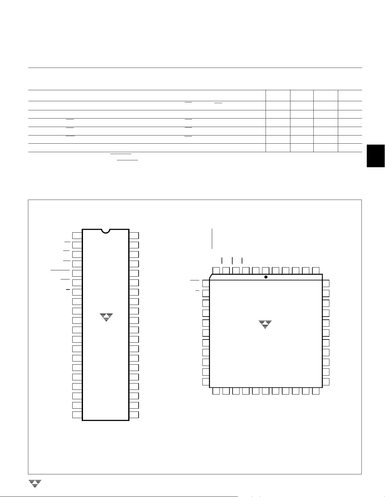
PIN CONFIGURATIONS
CS
CE
WR
RD
CONT/DEMAND
OVR/POL
L/H
DB7
DB6
DB5
DB4
DB3
DB2
DB1
DB0
BUSY
OSC
OSC
TEST
GND
1
2
3
4
5
6
7
8
9
10
TC850CPL
11
TC850IJL
12
13
14
15
16
17
1
18
2
19
20
40
39
38
37
36
35
34
33
32
31
30
29
28
27
26
25
24
23
22
21
V
DD
+
REF
1
+
C
REF1
–
C
REF1
–
REF
–
C
REF2
+
C
REF2
+
REF
2
+
IN
–
IN
COMMON
C
INTB
C
INTA
C
BUFA
C
BUFB
BUFFER
INT
IN
INT
OUT
V
SS
COMP
OVR/POL
L/H
DB7
DB6
DB5
NC
DB4
DB3
DB2
DB1
DB0
CONT/DEMAND
RD
6543 1442
7
8
9
10
11
12
13
18 19 20 21 23 24
OSC
BUSY
CE
WR
TC850CLW
TC850ILW
1
2
TEST
OSC
22
CS
GND
NC
NC
DD
V
COMP
1
+
43 42 41 40
25 26 27 28
REF
SS
V
+
REF1
C
OUT
INT
–
REF1
C
IN
INT
–
REF
39
38
37
36
35
34
33
3214
3115
3016
2917
BUFFER
–
C
REF2
+
C
REF2
+
REF
2
+
IN
–
IN
NC
COMMON
C
INTB
C
INTA
C
BUFA
C
BUFB
2
3
4
5
6
7
TELCOM SEMICONDUCTOR, INC.
NC = NO INTERNAL CONNECTION
8
3-79
Page 4

15-BIT, FAST-INTEGRATING CMOS
ANALOG-TO-DIGITAL CONVERTER
TC850
PIN DESCRIPTIONS
40-Pin DIP
Pin No. Symbol Description
1 CS Chip select, active HIGH. Logically ANDed with CE to enable read and write inputs. (See
2 CE Chip enable, active LOW. (See note 5.)
3 WR Write input, active LOW. When chip is selected (CS = HIGH and CE = LOW) and in demand
4 RD Read input, active LOW. When CS = HIGH and CE = LOW, a logic LOW on RD enables the
5 CONT/DEMAND Conversion control input. When CONT/DEMAND = LOW, conversions are initiated by the WR
6 OVR/POL Overrange/polarity data-select input. When making conversions in the demand mode (CONT/
7 L/H Low/high byte-select input. When CONT/DEMAND = LOW, this input controls whether low-
8 DB7 Most significant data bit output. When reading the A/D conversion result, the polarity,
9 – 15 DB6–DB0 Data outputs DB6–DB0. 3-state, bus compatible.
16 BUSY A/D conversion status output. BUSY goes to a logic HIGH at the beginning of the deintegrate
17 OSC
18 OSC
1
2
19 TEST For factory testing purposes only. Do not make external connection to this pin.
20 DGND Digital ground connection.
21 COMP Connection for comparator auto-zero capacitor. Bypass to VSS with 0.1 µF.
22 V
23 INT
24 INT
SS
OUT
IN
25 BUFFER Output of the input buffer. Connect to R
26 C
27 C
28 C
29 C
BUFB
BUFA
INTA
INTB
30 COMMON Analog common.
31 IN
–
30 COMMON Analog common.
REF2
REF2
REF1
REF1
DD
+
2
+
–
–
–
+
+
1
33 REF
34 C
35 C
36 REF
37 C
38 C
39 REF
40 V
NOTES: 4. This pin incorporates a pull-down resistor to DGND.
5. This pin incorporates a pull-up resistor to VDD.
note 4.)
mode (CONT/DEMAND = LOW), a logic LOW on WR starts a conversion. (See note 4.)
3-state data outputs. (See note 5.)
input. When CONT/DEMAND = HIGH, conversions are performed continuously. (See note 4.)
DEMAND = LOW), OVR/POL controls the data output on DB7 when the high-order byte is
active. (See note 5.)
byte or high-byte data is enabled on DB0 through DB7. (See note 5.)
overrange, and DB7 data are output on this pin. (See text.)
phase and goes LOW when conversion is complete. The falling edge of BUSY can be used to
generate a µP interrupt.
Crystal oscillator connection or external oscillator input.
Crystal oscillator connection.
Negative power supply connection, typically – 5V.
Output of the integrator amplifier. Connect to C
Input to the integrator amplifier. Connect to summing node of R
INT
.
INT
INT
and C
INT
.
.
Connection for buffer auto-zero capacitor. Bypass to VSS with 0.1 µF.
Connection to buffer auto-zero capacitor. Bypass to VSS with 0.1 µF.
Connection for integrator auto-zero capacitor. Bypass to VSS with 0.1 µF.
Connection for integrator auto-zero capacitor. Bypass to VSS with 0.1 µF.
Negative differential analog input.
Positive input for reference voltage V
Positive connection for V
Negative connection for V
reference capacitor.
REF2
reference capacitor.
REF2
REF2
. (V
REF2
= V
REF1
/64)
Negative input for reference voltages.
Negative connection for V
Positive connection for V
Positive input for V
REF1
reference capacitor.
REF1
reference capacitor.
REF1
.
Positive power supply connection, typically +5V.
3-80
TELCOM SEMICONDUCTOR, INC.
Page 5
15-BIT, FAST-INTEGRATING CMOS
ANALOG-TO-DIGITAL CONVERTER
1
TC850
THEORY OF OPERATION
The TC850 is a multiple-slope, integrating analog-todigital converter (ADC). The multiple-slope conversion process, combined with chopper-stabilized amplifiers, results
in a significant increase in ADC speed, while maintaining
very high resolution and accuracy.
Dual-Slope Conversion Principles
The conventional dual-slope converter measurement
cycle (shown in Figure 2A) has two distinct phases:
(1) Input signal integration
(2) Reference voltage integration (deintegration)
The input signal being converted is integrated for a fixed
time period, measured by counting clock pulses. An opposite polarity constant reference voltage is then integrated
until the integrator output voltage returns to zero. The
reference integration time is directly proportional to the input
signal.
In a simple dual-slope converter, complete conversion
requires the integrator output to "ramp-up" and "rampdown." Most dual-slope converters add a third phase, autozero. During auto-zero, offset voltages of the input buffer,
integrator, and comparator are nulled, thereby eliminating
the need for zero-offset adjustments.
Dual-slope converter accuracy is unrelated to the integrating resistor and capacitor values, as long as they are
stable during a measurement cycle. By converting the
unknown analog input voltage into an easily-measured
function of time, the dual-slope converter reduces the need
for expensive, precision passive components.
Noise immunity is an inherent benefit of the integrating
conversion method. Noise spikes are integrated, or averaged, to zero during the integration period. Integrating ADCs
are immune to the large conversion errors that plague
successive approximation converters in high-noise environments.
A simple mathematical equation relates the input signal,
reference voltage, and integration time:
t
SI
1
RC
VIN(t) dt = ,
∫
0
where: VR = Reference voltage
tSI = Signal integration time (fixed)
tRI = Reference voltage integration time (variable).
VR t
RC
RI
Multiple-Slope Conversion Principles
One limitation of the dual-slope measurement technique is conversion speed. In a typical dual-slope method,
the auto-zero and integrate times are each one-half of the
deintegrate time. For a 15-bit conversion, 214+214+2
(65,536) clock pulses are required for auto-zero, integrate,
and deintegrate phases, respectively. The large number of
clock cycles effectively limits the conversion rate to about
2.5 conversions per second, when a typical analog CMOS
fabrication process is used.
The TC850 uses a multiple-slope conversion technique
to increase conversion speed (Figure 2B). This technique
makes use of a two-slope deintegration phase and permits
15-bit resolution up to 40 conversions per second.
During the TC850's deintegration phase, the integration
capacitor is rapidly discharged to yield a resolution of 9 bits.
At this point, some charge will remain on the capacitor. This
remaining charge is then slowly deintegrated, producing an
2240
V
SS
COMMON
C
C
C
C
BUFFER
INT
C
BUFACBUFB
0.1
µF
–5V
REF
REF
REF
+
REF1
–
REF1
+
REF2
–
REF2
INT
OUT
TEST
IN
26
IN
100 MΩ
32
+
0.1
µF
31
30
39
33
36
38
37
34
35
25
24
23
19
0.01 µF INPUT
+1.6384V
+0.0265V
1 µF
1 µF
120 MΩ
R
INT
0.1µF
C
INT
NC
–
+
1
+
2
–
IN
+5V
20
V
DGND
DD
16
BUSY
8
DB7
9
DB6
10
DB5
11
DB4
12
DB3
13
DB2
14
DB1
15
DB0
1
CS
2
CE
3
WR
4
RD
5
CONT/DEMAND
6
OVR/POL
7
L/H
17
**
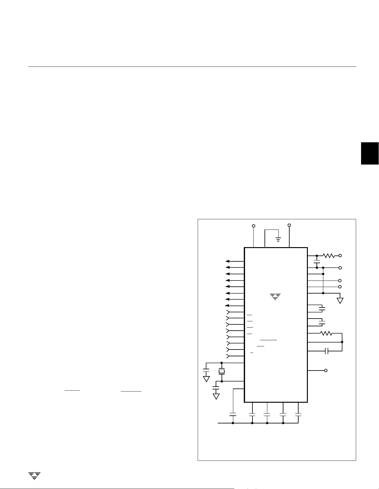
NOTES: Unless otherwise specified, all 0.1µF capacitors are film dielectric.
61.44 kHz
**
Ceramic capacitors are not recommended.
NC = No internal capacitors
*Polypropylene capacitors.
** 100pF Mica capacitors.
OSC
18
OSC
21
COMP
C
INTA
0.1
µF
Figure 1. Standard Circuit Configuration
1
2
C
INTB
28 2729
0.1
µF
TC850
0.1
µF
15
*
*
2
3
4
5
6
7
8
TELCOM SEMICONDUCTOR, INC.
3-81
Page 6

TC850
INTEGRATOR
OUTPUT
AUTO
ZERO
TIME
SIGNAL
INTEGRATE
REFERENCE
DEINTEGRATE
END OF
CONVERSION
0V
15-BIT, FAST-INTEGRATING CMOS
ANALOG-TO-DIGITAL CONVERTER
additional 6 bits of resolution. The result is 15 bits of
resolution achieved with only 29+26 (512 + 64, or 576) clock
pulses for deintegration. A complete conversion cycle occupies only 1280 clock pulses.
In order to generate "fast-slow" integration phases, two
voltage references are required. The primary reference
(V
) is set to one-half of the full-scale voltage (typically
REF1
V
= 1.6384V, and VFS = 3.2768V). The secondary
REF1
voltage reference (V
mV). To maintain 15-bit linearity, a tolerance of 0.5% for
V
is recommended.
REF2
) is set to V
REF2
/64 (typically 25.6
REF1
Figure 2A. Dual-Slope ADC Cycle
"FAST" REFERENCE
DEINTEGRATE
(9-BIT RESOLUTION)
SIGNAL
INTERGRATE
AUTO
INTEGRATOR
OUTPUT
IN
ZERO
TIME
Figure 2B. "Fast-Slow" Reference Deintegrate Cycle
C
REF1
+
REF1
+
C
REF1
DE
+
INT
DE1
(–)
DE1
(+)
DE
REF1
–
"SLOW" REFERENCE
DEINTEGRATE
(6-BIT RESOLUTION)
END OF
CONVERSION
0V
C
DE1
(–)
REF2
REF2
–
C
REF2
–
C
REF1
DE DE
ANALOG SECTION DESCRIPTION
The TC850 analog section consists of an input buffer
amplifier, integrator amplifier, comparator, and analog
switches. A simplified block diagram is shown in Figure 3.
Conversion Timing
Each conversion consists of three phases: (1) Zero
Integrator, (2) Signal Integrate, and (3) Reference Integrate
(or Deintegrate). Each conversion cycle requires 1280 internal clock cycles (Figure 4).
C
INT
INT
IN
INTEGRATOR*
–
+
INT
OUT
–
+
COMPARATOR*
DIGITAL
SECTION
+
DE1
(+)
C
–
REF2
BUFF
–
+
BUFFER*
R
INT
TO
COMMON
3-82
DE1
(+)
INT
–
IN
INT
DE1
(–)
Figure 3. Analog Section Simplified Schematic
DE2
(+)
DE2
(–)
Z1
*AUTO-ZEROED
AMPLIFIERS
TC850
TELCOM SEMICONDUCTOR, INC.
Page 7

15-BIT, FAST-INTEGRATING CMOS
ANALOG-TO-DIGITAL CONVERTER
1
TC850
1280 CLOCK CYCLES
INTERNAL
CLOCK
CONVERSION
PHASE
. . . . . . .
246 256 778
ZERO INTEGRATOR REFERENCE INTEGRATE
SIGNAL
INTEGRATE
Figure 4. Conversion Timing
Zero-Integrator Phase
During the zero-integrator phase, the differential input
signal is disconnected from the circuit by opening internal
analog gates. The internal nodes are shorted to analog
common (ground) to establish a zero-input condition. At the
same time, a feedback loop is closed around the input buffer,
integrator, and comparator. The feedback loop ensures the
integrator output is near 0V before the signal-integrate
phase begins.
During this phase, a chopper-stabilization technique is
used to cancel offset errors in the input buffer, integrator,
and comparator. Error voltages are stored on the C
C
, and COMP capacitors. The zero-integrate phase
INT
requires 246 clock cycles.
BUFF
Signal-Integrate Phase
The zero-integrator loop is opened and the internal
differential inputs are connected to IN+ and IN–. The differential input signal is integrated for a fixed time period. The
TC850 signal-integrate period is 256 clock periods, or counts.
The crystal oscillator frequency is 44 before clocking the
internal counters.
The integration time period is:
f
OSC
4
tSI = × 256
Reference-Integrate Phase
During reference-integrate phase, the charge stored on
the integrator capacitor is discharged. The time required to
discharge the capacitor is proportional to the analog input
voltage.
The reference integrate phase is divided into three
subphases: (1) fast, (2) slow, and (3) overrange deintegrate.
During fast deintegrate, V
analog common and V
charged reference capacitor (C
tor is rapidly discharged for a maximum of 512 internal clock
pulses, yielding 9 bits of resolution.
+
is connected across the previously-
IN
–
is internally connected to
IN
). The integrator capaci-
REF1
. . . . . . . . . . . . . .
During the slow deintegrate phase, the internal V
node is now connected to the C
residual charge on the integrator capacitor is further discharged a maximum of 64 clock pulses. At this point, the
analog input voltage has been converted with 15 bits of
resolution.
If the analog input is greater than full scale, the TC850
performs up to three overrange deintegrate subphases.
Each subphase occupies a maximum of 64 clock pulses.
The overrange feature permits analog inputs up to 192 LSBs
greater than full scale to be correctly converted. This feature
,
permits the user to digitally null up to 192 counts of input
offset, while retaining full 15-bit resolution.
In addition to 512 counts of fast, 64 counts of slow, and
192 counts of overrange deintegrate, the reference-integrate phase uses 10 clock pulses to permit internal nodes to
settle. Therefore, the reference integrate cycle occupies 778
clock pulses.
Pin Description (Analog)
Differential Inputs (IN+ and IN–)
The analog signal to be measured is applied at the IN
and IN– inputs. The differential input voltage must be within
the common-mode range of the converter. The input common-mode range extends from VDD –1.5V to VSS +1.5V.
Within this common-mode voltage range, an 86 dB CMRR
is typical.
The integrator output also follows the common-mode
voltage. The integrator output must not be allowed to saturate. A worst-case condition exists, for example, when a
large, positive common-mode voltage with a near full-scale
negative differential input voltage is applied. The negative
input signal drives the integrator positive when most of its
available swing has been used up by the positive commonmode voltage. For applications where maximum commonmode range is critical, integrator swing can be reduced. The
integrator output can swing within 0.4V of either supply
without loss of linearity.
capacitor, and the
REF2
2
3
+
IN
4
5
6
+
7
8
TELCOM SEMICONDUCTOR, INC.
3-83
Page 8

TC850
15-BIT, FAST-INTEGRATING CMOS
ANALOG-TO-DIGITAL CONVERTER
Differential Reference (V
REF
)
The TC850 requires two reference voltage sources in
order to generate the "fast-slow" deintegrate phases. The
main voltage reference (V
and REF– pins. The secondary reference (V
between the REF
+
and REF– pins.
2
) is applied between the REF
REF1
REF2
) is applied
The reference voltage inputs are fully differential, and
the reference voltage can be generated anywhere within the
power supply voltage of the converter. However, to minimize
roll-over error, especially at high conversion rates, keep the
reference common-mode voltage (i.e., REF–) near or at the
analog common potential. All voltage reference inputs are
high impedance. Average reference input current is typically
only 30pA.
Analog Common (COMMON)
Analog common is used as the IN– return during the
zero-integrator and deintegrate phases of each conversion.
If IN– is at a different potential than analog common, a
common-mode voltage exists in the system. This signal is
rejected by the 86 dB CMRR of the converter. However, in
most applications, IN– will be set at a fixed, known voltage
(power supply common, for instance). In this case, analog
common should be tied to the same point so that the
common-mode voltage is eliminated.
DIGITAL SECTION DESCRIPTION
+
1
The TC850 digital section consists of two sets of conversion counters, control and sequencing logic, clock oscillator
and divider, data latches, and an 8-bit, 3-state interface bus.
A simplified schematic of the bus interface logic is shown in
Figure 5.
Clock Oscillator
The TC850 includes a crystal oscillator on-chip. All that
is required is to connect a crystal across OSC1 and OSC
pins, and to add two inexpensive capacitors (Figure 1). The
oscillator output is ÷ 4 prior to clocking the A/D internal
counters. For example, a 100kHz crystal produces a system
clock frequency of 25kHz. Since each conversion requires
1280 clock periods, in this case the conversion rate will be
25,000/1280, or 19.5 conversions per second.
In most applications, however, an external clock is
divided down from the microprocessor clock. In this case,
the OSC1 pin is used as the external oscillator input and
OSC2 is left unconnected. The external clock driver should
swing from digital ground to VDD. The ÷4 function is active for
both external clock and crystal oscillator operations.
2
DBO–DB7
L/H
RD
CE
CS
POL/OVR
WR
CONT/
DEMAND
3-STATE
BUFFER
8
OUTPUT
ENABLE
OCTAL
2-INPUT
8 7
MUX
SELECT
TC850
8
SELECT
2-INPUT
MUX
START
CONVERSION
END OF
CONVERSION
LOW-BYTE
UP/DOWN
COUNTER
HIGH-BYTE
UP/DOWN
COUNTER
TO A/D
CONTROL
LOGIC
POLARITY
OVERANGE
3-84
Figure 5. Bus Interface Simplified Schematic
TELCOM SEMICONDUCTOR, INC.
Page 9

15-BIT, FAST-INTEGRATING CMOS
ANALOG-TO-DIGITAL CONVERTER
1
TC850
Digital Operating Modes
Two modes of operation are available with the TC850,
continuous conversions and on-demand. The operating
mode is controlled by the CONT/DEMAND input. The bus
interface method is different for continuous and demand
modes of operation.
Demand Mode Operation
When CONT/DEMAND is low, the TC850 performs one
conversion each time the chip is selected and the WR input
is pulsed low. Data is valid on the falling edge of the BUSY
output and can be accessed using the interface truth table
(Table 1).
Table 1. Bus Interface Truth Table
CE•CS RD CONT/DEMAND L/H OVR/POL DB7 DB6–DB0
Pins 1 and 2 Pin 4 Pin 5 Pin 7 Pin 6 Pin 8 Pin 9-Pin 15 (Note 1)
0 0 0 0 0 "1" = Input Positive Data Bits 14 – 8
0 0 0 0 1 "1" = Input Overrange Data Bits 14 – 8
0 0 0 1 X Data Bit 7 Data Bits 6 – 0
0 0 1 X X Note 3
0 1 X X X High-Impedance State
1 X X X X High-Impedance State
NOTES: 1. Pin numbers refer to 40-pin DIP.
2. Extended overrange operation: Although rated at 15 bits (±32,767 counts) of resolution, the TC850 provides an additional 191 counts
above full scale. For example, with a full-scale input of 3.2768V, the maximum analog input voltage which will be properly converted is
3.2958V. The extended resolution is signified by the overrange bit being high and the low-order byte contents being between 0 and 190.
For example, with a full-scale voltage of 3.2768V:
V
IN
3.2767V Low 255
3.2768V High 000
3.2769V High 001
3.2867V High 099
3. Continuous mode data transfer:
a. In continuous mode, data MUST be read in three sequential bytes after the BUSY output goes low:
(1) The first byte read will be the high-order byte, with DB7 = polarity.
(2) The second byte read will contain the low-order byte.
(3) The third byte read will again be the high-order byte, but with DB7 = overrange.
b. All three data bytes must be read within 443-1/2 clock cycles after the falling edge of BUSY.
c. The RD input must go high after each byte is read, so that the internal byte counter will be incremented. However, the CS and CE
inputs can remain enabled through the entire data transfer sequence.
Overrange Bit Low Byte Data Bits 14–8
10
10
10
10
Continuous Mode Operation
When CONT/DEMAND is high, the TC850 continuously
performs conversions. Data will be valid on the falling edge
of the BUSY output, and remains valid for 443-1/2 clock
cycles.
The low/high (L/H) byte-select and overrange/polarity
(OVR/POL) inputs are disabled during continuous mode
operation. Data must be read in three consecutive bytes, as
shown in Table I.
NOTE: In continuous mode, the conversion result must be read within 4431/2 clock cycles of the BUSY output falling edge. After this time (i.e., 1/2
clock cycle before BUSY goes high) the internal counters are reset and the
data is lost.
(Note 2)
127
10
0
10
0
10
0
10
2
3
4
5
6
TELCOM SEMICONDUCTOR, INC.
7
8
3-85
Page 10

TC850
15-BIT, FAST-INTEGRATING CMOS
ANALOG-TO-DIGITAL CONVERTER
Pin Description (Digital)
Chip Select and Chip Enable (CS and CE)
The CS and CE inputs permit easy interfacing to a
variety of digital bus systems. CE is active LOW while CS is
active HIGH. These inputs are logically ANDed internally
and are used to enable the RD and WR inputs.
Write Enable Input (WR)
The write input is used to initiate a conversion when the
TC850 is in demand mode. CS and CE must be active for the
WR input to be recognized. The status of the data bus is
meaningless during the WR pulse, because no data is
actually written into the TC850.
Read Enable Input (RD)
The read input, combined with CS and CE, enables the
3-state data bus outputs. Also, in continuous mode, the
rising edge of the RD input activates an internal byte counter
to sequentially read the three data bytes.
Low/High Byte Select (L/H)
The L/H input determines whether the low (least significant) byte or high (most significant) byte of data is placed on
the 3-state data bus. This input is meaningful only when the
TC850 is in the demand mode. In the continuous mode, data
must be read in three predetermined bytes, so the L/H input
is ignored.
Overrange/Polarity Bit Select (OVR/POL)
The TC850 provides 15 bits of resolution, plus polarity
and overrange bits. Thus, 17 bits of information must be
transferred on an 8-bit data bus. To accomplish this, the
overrange and polarity bits are multiplexed onto data bit DB7
of the most significant byte. When OVR/POL is HIGH, DB7
of the high byte contains the overrange status (HIGH =
analog input overrange, LOW = input within full scale). When
OVR/POL is LOW, DB7 is HIGH for positive analog input
polarity and LOW for negative polarity. The OVR/POL input
is meaningful only when CS, CE, and RD are active, and L/
H is LOW (i.e., the most significant byte is selected). OVR/
POL is ignored when the TC850 is in continuous mode.
Continuous/Demand Mode Input (CONT/DEMAND)
This input controls the TC850 operating mode. When
CONT/DEMAND is HIGH, the TC850 performs conversions
continuously. In continuous mode, data must be read in the
prescribed sequence shown in Table I. Also, all three data
bytes must be read within 443-1/2 internal clock cycles after
the BUSY output goes low. After 443-1/2 clock cycles data
will be lost.
When CONT/DEMAND is LOW, the TC850 begins a
conversion each time CS and CE are active and WR is
pulsed LOW. The conversion is complete and data can be
read after the falling edge of the BUSY output. In demand
mode, data can be read in any sequence, and remains valid
until WR is again pulsed LOW.
Busy Output (BUSY)
The BUSY output is used to convey an end-of-conversion to external logic. BUSY goes HIGH at the beginning of
the deintegrate phase and goes LOW at the end of the
conversion cycle. Data is valid on the falling edge of BUSY.
The output-high period is fixed at 836 clock periods, regardless of the analog input value. BUSY is active during
continuous and demand mode operation.
This output can also be used to generate an end-ofconversion interrupt in µP-based systems. Noninterruptdriven systems can poll BUSY to determine when data is
valid.
ANALOG SECTION APPLICATIONS
Component Selection
Reference Voltage
The typical value for reference voltage V
This value yields a full-scale voltage of 3.2768V and resolution of 100µV per step. The V
V
by 64. Thus, typical V
REF1
25.6mV. The V
value should be adjusted within ±1% to
REF2
value is derived by dividing
REF2
value is 1.6384V/64, or
REF2
maintain 15-bit accuracy for the total conversion process;
i.e.,
V
V
REF2
REF1
= ±1%.
64
The reference voltage is not limited to exactly 1.6384V,
however, because the TC850 performs a ratiometric conversion. Therefore, the conversion result will be:
V
Digital counts = • 16384.
V
IN
REF1
The full-scale voltage can range from 3.2V to 3.5V. Fullscale voltages of less than 3.2V will result in increased noise
in the least significant bits, while a full-scale above 3.5V will
exceed the input common-mode range.
Integration Resistor
The TC850 buffer supplies 25µA of integrator charging
current with minimal linearity error. R
V
R
INT
FULL SCALE
= .
25 µA
is easily calculated:
INT
For a full-scale voltage of 3.2768V, values of R
between 120kΩ and 150kΩ are acceptable.
is 1.6384V.
REF1
INT
3-86
TELCOM SEMICONDUCTOR, INC.
Page 11

15-BIT, FAST-INTEGRATING CMOS
ANALOG-TO-DIGITAL CONVERTER
1
TC850
Integration Capacitor
The integration capacitor should be selected to produce
an integrator swing of ≈4V at full scale. The capacitor value
is easily calculated:
V
FS
C = • ,
R
INT
where f
and VFS is the maximum input voltage.
The integration capacitor should be selected for low
dielectric absorption to prevent roll-over errors. A polypropylene, polyester or polycarbonate dielectric capacitor is
recommended.
Reference Capacitors
The reference capacitors require a low leakage dielectric, such as polypropylene, polyester or polycarbonate. A
value of 1µF is recommended for operation over the temperature range. If high-temperature operation is not required, the C
Auto-Zero Capacitors
Five capacitors are required to auto-zero the input
buffer, integrator amplifier, and comparator. Recommended
capacitors are 0.1µF film dielectric (such as polyester or
polypropylene). Ceramic capacitors are not recommended.
is the crystal or external oscillator frequency
CLOCK
values can be reduced.
REF
4 • 256
4V • f
CLOCK
f
= f
CLOCK
where f
sents the clock divider, and 256 is the number of integrate
cycles.
For example, 60Hz noise will be rejected with a clock
frequency of 61.44kHz, giving a conversion rate of 12
conversions/sec. Integer submultiples of 61.44kHz (such as
30.72kHz, etc.) will also reject 60Hz noise. For 50Hz noise
rejection, a 51.2kHz frequency is recommended.
If noise rejection is not important, other clock frequencies can be used. The TC850 will typically operate at
conversion rates ranging from 3 to 40 conversions/sec,
corresponding to oscillator frequencies from 15.36kHz to
204.8kHz.
is the noise frequency to be rejected, 4 repre-
NOISE
10 MΩ
TC850
17
61.44 kHz
100 pF 100 pF
NOISE
× 4 × 256,
÷
4
18
SYSTEM
CLOCK
2
3
4
5
DIGITAL SECTION APPLICATION
Oscillator
The TC850 may operate with a crystal oscillator. The
crystal selected should be designed for a Pierce oscillator,
such as an AT-cut quartz crystal. The crystal oscillator
schematic is shown in Figure 6.
Since low frequency crystals are very large and ceramic
resonators are too lossy, the TC850 clock should be derived
from an external source, such as a microprocessor clock.
The clock should be input on the OSC1 pin and no connection should be made to the OSC2 pin. The external clock
should swing between DGND and VDD.
Since oscillator frequency is ÷ 4 internally and each
conversion requires 1280 internal clock cycles, the conversion time will be:
Conversion time = f
An important advantage of the integrating ADC is the
ability to reject periodic noise. This feature is most often
used to reject line frequency (50Hz or 60Hz) noise. Noise
rejection is accomplished by selecting the integration period
equal to one or more line frequency cycles. The desired
clock frequency is selected as follows:
CLOCK
× 4 × 1280.
Figure 6. Crystal Oscillator Schematic
Data Bus Interfacing
The TC850 provides an easy and flexible digital interface. A 3-state data bus and six control inputs permit the
TC850 to be treated as a memory device, in most applications. The conversion result can be accessed over an 8-bit
bus or via a µP I/O port.
A typical µP bus interface for the TC850 is shown in
Figure 7. In this example, the TC850 operates in the demand
mode, and conversion begins when a write operation is
performed to any decoded address space. The BUSY
output interrupts the µP at the end-of-conversion.
The A/D conversion result is read as three memory
bytes. The two LSBs of the address bus select high/low byte
and overrange/polarity bit data, while high-order address
lines enable the CE input.
Figure 8 shows a typical interface to a µP I/O port or
single-chip µC. The TC850 operates in the continuous
mode, and can either interrupt the µC/µP or be polled with an
input pin.
6
7
8
TELCOM SEMICONDUCTOR, INC.
3-87
Page 12

TC850
TC850
CONT/DEMAND
TC850
DB0
DB1
DB2
DB3
DB4
DB5
DB6
DB7
CS
L/H
OVR/POL
RD
WR
BUSY
CS
ADDRESS
X00
X01
X10
Figure 7. Interface to Typical µP Data Bus
DB0
DB1
DB2
DB3
DB4
DB5
DB6
DB7
ADDRESS
DECODE
+5V
DATA BUS
HIGH BYTE AND POLARITY
LOW BYTE
HIGH BYTE AND OVERRANGE
DB0
DB1
DB2
DB3
DB4
DB5
DB6
DB7
A2
. . .
A15
A0
A1
RD
WR
INTERRUPT
PA0
PA1
PA2
PA3
PA4
PA5
PA6
PA7
µP
µC OR µP
I/O PORT
15-BIT, FAST-INTEGRATING CMOS
ANALOG-TO-DIGITAL CONVERTER
Since the PA0–PA7 inputs are dedicated to reading
A/D data, the A/D CS/CE inputs can be enabled continuously. In continuous mode, data must be read in 3 bytes, as
shown in Table I. The required RD pulses are provided by a
µC/µP output pin.
The circuit of Figure 8 can also operate in the demand
mode, with the start-up conversion strobe generated by a
µC/µP output pin. In this case, the L/H and CONT/DEMAND
inputs can be controlled by I/O pins and the RD input
connected to digital ground.
Demand Mode Interface Timing
When CONT/DEMAND input is LOW, the TC850 performs a conversion each time CE and CS are active and WR
is strobed LOW.
The demand mode conversion timing is shown in Figure
9. BUSY goes LOW and data is valid 1155 clock pulses after
WR goes LOW. After BUSY goes low, 125 additional clock
cycles are required before the next conversion cycle will
begin.
Once conversion is started, WR is ignored for 1100
internal clock cycles. After 1100 clock cycles, another WR
pulse is recognized and initiates a new conversion when the
present conversion is complete. A negative edge on WR is
required to begin conversion. If WR is held LOW, conversions will not occur continuously.
The A/D conversion data is valid on the falling edge of
BUSY, and remains valid until one-half internal clock cycle
before BUSY goes HIGH on the succeeding conversion.
BUSY can be monitored with an I/O pin to determine end of
conversion, or to generate a µP interrupt.
In demand mode, the three data bytes can be read in
any desired order. The TC850 is simply regarded as three
bytes of memory and accessed accordingly. The bus output
timing is shown in Figure 10.
BUSY
RD
CONT/DEMAND
CS
CS WR
NC
Figure 8. Interface to Typical µP I/O Port or Single-Chip µC
3-88
+5V
INTERRUPT
PB0
Continuous Mode Interface Timing
When the CONT/DEMAND input is HIGH, the TC850
performs conversions continuously. Data will be valid on the
falling edge of BUSY, and all three bytes must be read within
443-1/2 internal clock cycles of BUSY going LOW. The
timing diagram is shown in Figure 11.
In continuous mode, OVR/POL and L/H byte-select
inputs are ignored. The TC850 automatically cycles through
three data bytes, as shown in Table I. Bus output timing in
the continuous mode is shown in Figure 12.
TELCOM SEMICONDUCTOR, INC.
Page 13

15-BIT, FAST-INTEGRATING CMOS
ANALOG-TO-DIGITAL CONVERTER
1
TC850
CS
.
CE
INTERNAL
CLOCK
.
CS
CE
WR
BUSY
DB0-DB7
. . . .
319 CLOCK
CYCLES
PREVIOUS CONVERSION
DATA VALID
t
CE
t
RE
. . . . . . . .
1100 CLOCK CYCLES
WR PULSES ARE IGNORED
836 CLOCK CYCLES
DATA MEANINGLESS
Figure 9. Conversion Timing, Demand Mode
NEXT CONVERT
COMMAND WILL
BE RECOGNIZED
125 CLOCK
CYCLES
NEW CONVERSION DATA VALID
t
DHC
t
DHR
NEXT
CONVERSION
CAN BEGIN
2
3
4
RD
DB0-DB6
DB7
OVR/POL
L/H
*
HI-Z
HI-Z
NOTE: CONT/DEMAND = LOW
*RD (as well as CS and CE) can go HIGH after each byte is read (i.e., in a µP bus interface)
or remain LOW during the entire DATA-READ sequence (i.e., µP I/O port interface).
DATA BITS 8 TO 14 HIGH IMPEDANCE
"1"= INPUT
OVERRANGE
t
OP
Figure 10. Bus Output Timing, Demand Mode
"1"= POSITIVE
POLARITY
t
LH
DATA BITS
0 T0 6
DATA BIT 7
5
6
HIGH IMPEDANCE
DONT' CARE
7
DONT' CARE
8
TELCOM SEMICONDUCTOR, INC.
3-89
Page 14

TC850
15-BIT, FAST -INTEGRATING CMOS
ANALOG-TO-DIGITAL CONVERTER
INTERNAL
CLOCK
BUSY
DB0-DB7
CONT/DEMAND
BUSY
RD
. . . . . . .
836 CLOCK CYCLES
DATA MEANINGLESS
Figure 11. Conversion Timing, Continuous Mode
t
WRE
t
RE
1280 INTERNAL CLOCK CYCLES
t
WRD
. . . . . . . . . .
443-1/2 CLOCK
CYCLES
DATA VALID
1/2 CLOCK CYCLE
DATA
MEANINGLESS
3-90
DB0-DB7
HI-Z
NOTES: CS = HIGH; CE = LOW
DATA BITS 8-14
POLARITY
DATA BITS 0-7
Figure 12. Bus Output Timing, Continuous Mode
DATA BITS 8-14
OVERRANGE
HIGH IMPEDANCE
STATE
TELCOM SEMICONDUCTOR, INC.
 Loading...