

Page 1
A/D CONVERTER WITH BAR GRAPH DISPLAY OUTPUT
1
TC826
2
FEATURES
■ Bipolar A/D Conversion
■ 2.5% Resolution
■ Direct LCD Display Drive
■ ‘Thermometer’ Bar or Dot Display
■ 40 Data Segments Plus Zero
■ Overrange Plus Polarity Indication
■ Precision On–Chip Reference ................ 35ppm/°C
■ Differential Analog Input
■ Low Input Leakage .......................................... 10pA
■ Display Flashes on Overrange
■ Display Hold Mode
■ Auto–Zero Cycle Eliminates Zero Adjust
Potentiometer
■ 9V Battery Operation
■ Low Power Consumption ............................ 1.1mW
■ 20mV to 2.0 V Full–Scale Operation
■ Non–Multiplexed LCD Drive for Maximum
Viewing Angle
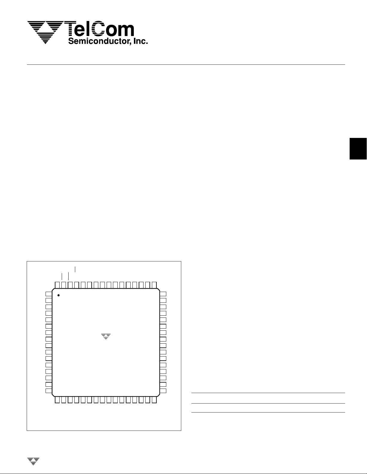
PIN CONFIGURATION
BAR 35
BAR 36
BAR 37
BAR 38
BAR 39
BAR 40
OR
POL –
BAR/DOT
HOLD
ANALOG
COMMON
– IN
REF IN
+
C
REF
–
C
REF
V
V
BUF
C
V
V
OSC1
OSC2
BAR 0
TEST
NC
626364 49
61
NC
1
2
+IN
3
4
5
6
7
8
DD
9
10
AZ
11
INT
SS
12
13
14
BP
15
16
NC
BAR 1
BAR 2
BAR 3
BAR 4
TC826CBU
BAR 6
BAR 5
BAR 7
BAR 8
26
BAR 9
27
BAR 10
BAR 11
BAR 34
302928
BAR 12
BAR 33
5051255224532354225521562057195818591760
31
BAR 13
BAR 32
32
BAR 14
BAR 31
BAR 15
48
NC
47
BAR 30
46
BAR 29
45
BAR 28
44
BAR 27
43
BAR 26
42
BAR 25
41
BAR 24
40
BAR 23
39
BAR 22
38
BAR 21
37
BAR 20
36
BAR 19
35
BAR 18
34
BAR 17
33
BAR 16
GENERAL DESCRIPTION
In many applications a graphical display is preferred
over a digital display. Knowing a process or system operates, for example, within design limits is more valuable than
a direct system variable readout. A bar or moving dot display
supplies information precisely without requiring further interpretation by the viewer.
The TC826 is a complete analog–to–digital converter
with direct liquid crystal (LCD) display drive. The 40 LCD
data segments plus zero driver give a 2.5% resolution bar
display. Full–scale differential input voltage range extends
from 20mV to 2V. The TC826 sensitivity is 500µv. A low drift
35 ppm/°C internal reference, LCD backplane oscillator and
driver, input polarity LCD driver, and overrange LCD driver
make designs simple and low cost. The CMOS design
required only 125µA from a 9V battery. In +5V systems a
TC7660 DC to DC converter can supply the –5V supply. The
differential analog input leakage is a low 10pA.
Two display formats are possible. The BAR mode
display is like a ‘thermometer’ scale. The LCD segment
driver that equals the input plus all below it are on. The DOT
mode activates only the segment equal to the input. In either
mode the polarity signal is active for negative input signals.
An overrange input signal causes the display to flash and
activates the overrange annunciator. A hold mode can be
selected that freezes the display and prevents updating.
The dual slope integrating conversion method with
auto–zero phase maximizes noise immunity and eliminates
zero–scale adjustment potentiometers. Zero–scale drift is a
low 5 µV/°C. Conversion rate is typically 5 per second and
is adjustable by a single external resistor.
A compact, 0.5" square, flat package minimizes PC
board area. The high pin count LSI package makes multiplexed LCD displays unnecessary. Low cost, direct drive
LCD displays offer the widest viewing angle and are readily
available. A standard display is available now for TC826
prototyping work.
ORDERING INFORMATION
Part No. Package Temperature
TC826CBU 64–Pin PFP 0°C to +70°C
3
4
5
6
7
TELCOM SEMICONDUCTOR, INC.
8
TC826-6 11/6/96
3-171
Page 2

TC826
A/D CONVERTER WITH
BAR GRAPH DISPLAY OUTPUT
ABSOLUTE MAXIMUM RATINGS*
Supply Voltage (V+ to V–)............................................15V
Analog Input Voltage (either input)
Power Dissipation (TA ≤ 70°C)
64-Pin Flat Package .........................................1.14W
Operating Temperature
(1)
................... V+ to V
*Static-sensitive device. Unused devices must be stored in conductive
material. Protect devices from static discharge and static fields. Stresses
above those listed under Absolute Maximum Ratings may cause perma-
–
nent damage to the device. These are stress ratings only and functional
operation of the device at these or any other conditions above those
indicated in the operational sections of the specifications is not implied.
Exposure to Absolute Maximum Rating Conditions for extended periods
may affect device reliability.
‘C’ Devices.............................................0°C to +70°C
Storage Temperature ............................– 65°C to +150°C
Lead Temperature (Soldering, 10 sec) .................+300°C
ELECTRICAL CHARACTERISTICS:
unless otherwise stated VS = 9V; R
= 430 kΩ; TA = 25°C; Full–Scale = 20 mV.
OSC
No. Symbol Parameter Test Conditions Min Typ Max Unit
1 — Zero Input VIN = 0.0V – 0 ±0 +0 Display
2 — Zero Reading Drift VIN = 0.0V — 0.2 1 µV/°C
0°C ≤ TA ≤ +70°C
3 NL Linearity Error Max Deviation From – 1 0.5 +1 Count
Best Straight Line
4 R/O Rollover Error –VIN = +V
IN
5 EN Noise VIN = 0V — 60 — µV
6 ILK Input Leakage Current VIN = 0V — 10 20 pA
7 CMRR Common–Mode VCM = ±1V — 50 — µV/V
Rejection Ratio VIN = 0V
8 — Scale Factor 0 ≤ T
≤ +70°C — 1 — ppm/°C
A
Temperature Coefficient External Ref. Temperature
Coefficient = 0 ppm/°C
9 VCTC Analog Common 250kΩ Between — 35 100 ppm/°C
Temperature Coefficient Common and V
+
0°C ≤ TA ≤ +70°C
10 V
COM
Analog Common 250kΩ Between 2.7 2.9 3.35 V
Voltage Common and V
DD
11 VSD LCD Segment 4 5 6 V
Drive Voltage
12 VBD LCD Backplane 4 5 6 V
Drive Voltage
13 I
NOTES: 1. Input voltages may exceed the supply voltages when
DD
the input current is limited to 100µA.
2. Static sensitive device. Unused devices should be
stored in conductive material to protect devices from
static discharge and static fields.
3. Backplane drive is in phase with segment drive for ‘off’ segment and 180°C out of phase for ‘on’ segment. Frequency is 10 times
conversion rate.
4. Logic input pins 58, 59, and 60 should be connected through 1MΩ series resistors to VSS for logic 0.
Power Supply Current — 125 175 µA
– 1 0 +1 Count
P–P
P–P
P–P
3-172
TELCOM SEMICONDUCTOR, INC.
Page 3

A/D CONVERTER WITH
BAR GRAPH DISPLAY OUTPUT
PIN DESCRIPTION
1
TC826
Pin No.
(64-Plastic
Quad Flat
Package) Symbol Description
1NC
2 ANALOG Establishes the internal analog ground point. Analog common is set to 2.9V below the positive supply
COMMON by an internal zener reference circuit. The voltage difference beween V
used to supply the TC826 voltage reference input at REF IN (Pin 5).
3 +IN Positive analog signal input.
4 -IN Negative analog signal input.
5 REF IN Reference voltage positive input. Measured relative ato analog-common. REF IN ≈ Full-Scale/2.
BUF
AZ
INT
SS
+
Reference capacitor connection.
–
Reference capacitor connection.
Buffer output. Integration resistor connection.
Negative comparator input. Auto-zero capacitor connection.
Integrator output. Integration capacitor connection.
Negative supply terminal.
6 CREF
7 CREF
8VDDPositive supply terminal.
9V
10 C
11 V
12 V
13 OSC1 Oscillator resistor (ROSC) connection.
14 OSC2 Oscillator resistor (ROSC) connection.
15 BP LCD Backplane driver.
16 BAR 0 LCD Segment driver: Bar 0
17 NC
18 BAR 1 LCD Segment driver: Bar 1
19 BAR 2 LCD Segment driver: Bar 2
20 BAR 3 LCD Segment driver: Bar 3
21 BAR 4 LCD Segment driver: Bar 4
22 BAR 5 LCD Segment driver: Bar 5
23 BAR 6 LCD Segment driver: Bar 6
24 BAR 7 LCD Segment driver: Bar 7
25 BAR 8 LCD Segment driver: Bar 8
26 BAR 9 LCD Segment driver: Bar 9
27 BAR 10 LCD Segment driver: Bar 10
28 BAR 11 LCD Segment driver: Bar 11
29 BAR 12 LCD Segment driver: Bar 12
30 BAR 13 LCD Segment driver: Bar 13
31 BAR 14 LCD Segment driver: Bar 14
32 BAR 15 LCD Segment driver: Bar 15
33 BAR 16 LCD Segment driver: Bar 16
34 BAR 17 LCD Segment driver: Bar 17
35 BAR 18 LCD Segment driver: Bar 18
36 BAR 19 LCD Segment driver: Bar 19
37 BAR 20 LCD Segment driver: Bar 20
38 BAR 21 LCD Segment driver: Bar 21
39 BAR 22 LCD Segment driver: Bar 22
40 BAR 23 LCD Segment driver: Bar 23
and analog-common can be
DD
2
3
4
5
6
7
8
TELCOM SEMICONDUCTOR, INC.
3-173
Page 4

A/D CONVERTER WITH
BAR GRAPH DISPLAY OUTPUT
TC826
PIN DESCRIPTION (Cont.)
Pin No.
(64-Plastic
Quad Flat
Package) Symbol Description
41 BAR 24 LCD Segment driver: Bar 24
42 BAR 25 LCD Segment driver: Bar 25
43 BAR 26 LCD Segment driver: Bar 26
44 BAR 27 LCD Segment driver: Bar 27
45 BAR 28 LCD Segment driver: Bar 28
46 BAR 29 LCD Segment driver: Bar 29
47 BAR 30 LCD Segment driver: Bar 30
48 NC
49 BAR 31 LCD Segment driver: Bar 31
50 BAR 32 LCD Segment driver: Bar 32
51 BAR 33 LCD Segment driver: Bar 33
52 BAR 34 LCD Segment driver: Bar 34
53 BAR 35 LCD Segment driver: Bar 35
54 BAR 36 LCD Segment driver: Bar 36
55 BAR 37 LCD Segment driver: Bar 37
56 BAR 38 LCD Segment driver: Bar 38
57 BAR 39 LCD Segment driver: Bar 39
58 BAR 40 LCD Segment driver: Bar 40
59 OR LCD segment driver that indicated input out–of–range condition.
60 POL– LCD segment driver that indicates input signal is negative.
61 Input logic signal that selects bar or dot display format. Normally in bar mode. Connect to V
1MΩ resistor for Dot format.
62 Input logic signal that prevents display from changing. Pulled high internally to inactive state.
Connect to VSS through 1MΩ series resistor for HOLD mode operation.
63 Input logic signal. Sets TC826 to BAR display mode. BAR 0 to 40, plus OR flash on and off. The POL–
LCD driver is on. Pulled high internally to inactive state. Connect to VSS with 1 MΩ series resistor to
activate.
64 NC
through
SS
3-174
TELCOM SEMICONDUCTOR, INC.
Page 5

A/D CONVERTER WITH
H
BAR GRAPH DISPLAY OUTPUT
C
1
TC826
INT
2
1MΩ
1MΩ
1MΩ
9V
COMPONENT
R
INT
C
INT
C
REF
C
AZ
C
AZ
TC826
20 mV
C
AZ
–IN +IN
R
INT
V
61
BAR/DOT
62
HOLD
63
TEST
12
V
SS
V
DD
R
1
2V
FULL–SCALE
2MΩ 20kΩ 20kΩ
0.033µf 0.033 µf 0.033 µf
1µf1µf1µf
0.068µf 0.068µf 0.014µfR
200 mV
FULL–SCALE
Figure 1. Typical TC826 Circuit Connection
BUF
REFINANALOG
COMMON –IN +IN
58 2 43 60
R
2
FULL–SCALE
11109
V
INT C
BAR0–
BAR40 POL–
SEGMENT DRIVE
+ R2= 250kΩ
1
6
+
REF
–
C
OSC1
OSC2
7
REF
13
14
15
BP
59
OR
–OR
C
REF
1.0µf
R
OSC
430kΩ
BACKPLANE
41 SEGMENT
LCD BAR GRAP
3
4
5
6
TELCOM SEMICONDUCTOR, INC.
7
8
3-175
Page 6

TC826
A/D CONVERTER WITH
BAR GRAPH DISPLAY OUTPUT
DUAL SLOPE CONVERSION PRINCIPLES
The TC826 is a dual slope, integrating analog–to–digital
converter. The conventional dual slope converter measurement cycle has two distinct phases:
• Input Signal Integration
• Reference Voltage Integration (Deintegration)
The input signal being converted is integrated for a fixed
time period (TSI). Time is measured by counting clock
pulses. An opposite polarity constant reference voltage is
then integrated until the integrator output voltage returns to
zero. The reference integration time is directly proportional
to the input signal (TRI). (Figure 2).
In a simple dual slope converter a complete conversion
requires the integrator output to ‘ramp–up’ and ‘ramp–
down’.
A simple mathematical equation relates the input signal
reference voltage and integration time:
T
SI
1
RC
∫
V
(t) dt =
I N
0
Where:
VR = Reference Voltage
V
= Signal Integration Time (Fixed)
SI
TRI = Reference Voltage Integration Time (Variable)
=V
For a constant VIN:
V
I N
VRT
R I
RC
T
R I
R
T
S I
The dual slope converter accuracy is unrelated to the
integrating resistor and capacitor values as long as they are
stable during a measurement cycle. An inherent benefit is
noise immunity. Noise spikes are integrated or averaged to
zero during the integration periods. Integrating ADCs are
immune to the large conversion errors that plague successive approximation converters in high noise environments.
Interfering signals with frequency components at multiples
of the averaging period will be attenuated. (Figure 3.)
The TC826 converter improves the conventional dual
slope conversion technique by incorporating an auto-zero
phase. This phase eliminates zero-scale offset errors and
drift. A potentiometer is not required to obtain a zero output
for zero input.
30
T = MEASUREMENT
PERIOD
20
10
NORMAL MODE REJECTION (dB)
0
0.1/T 1/T 10/T
INPUT FREQUENCY
Figure 3. Normal-Mode Rejection of Dual Slope Converter
C
3-176
ANALOG
INPUT
SIGNAL
OUTPUT
INTEGRATOR
FIXED SIGNAL
INTEGRATE
+/–
REF
VOLTAGE
TIME
INTEGRATOR
R
–
–
+
+
SWITCH DRIVER
POLARITY CONTROL
VIN≈ 1/2 V
VIN≈ 1/4 V
VARIABLE
REFERENCE
INTEGRATE
TIME
Figure 2. Basic Dual Slope Converter
PHASE CONTROL
FULL–SCALE
FULL–SCALE
COMPARATOR
CONTROL
LOGIC
CLOCK
COUNTER
DISPLAY
TELCOM SEMICONDUCTOR, INC.
Page 7

A/D CONVERTER WITH
BAR GRAPH DISPLAY OUTPUT
1
TC826
THEORY OF OPERATION
Analog Section
In addition to the basic signal integrate and deintegrate
cycles discussed above, the TC826 incorporates an autozero cycle. This cycle removes buffer amplifier, integrator,
and comparator offset voltage error terms from the conversion. A true digital zero reading results without external
adjusting potentiometers. A complete conversion consists
of three cycles: an auto-zero, signal integrate and reference
cycle. (Figures 4 and 5.)
Auto-Zero Cycle
During the auto-zero cycle the differential input signal is
disconnected from the circuit by opening internal analog
gates. The internal nodes are shorted to analog common
(internal analog ground) to establish a zero input condition.
Additional analog gates close a feedback loop around the
integrator and comparator. This loop permits comparator
REF IN
56 7910
C
REF
offset voltage error compensation. The voltage level established on CAZ compensates for device offset voltages.
The auto-zero cycle length is 19 counts minimum.
Unused time in the deintegrate cycle is added to the autozero cycle.
Signal Integration Cycle
The auto-zero loop is opened and the internal differential inputs connect to +IN and –IN. The differential input
signal is integrated for a fixed time period. The TC826 signal
integration period is 20 clock periods or counts. The externally set clock frequency is divided by 32 before clocking the
internal counters. The integration time period is:
32
Where:
TSI =
F
F
= External Clock Frequency
OSC
R
INT
CAZC
OSC
11
x 20
INT
V
DD
8
2
3
4
+ INPUT
ANALOG
COMMON
– INPUT
AZ
3
INT
DE– DE+
AZ
–
+
BUFFER
INTEGRATOR
–
+
COMPARATOR
+
–
AZ
CMPTR
TO DIGITAL
SECTION
5
6
AZ
2
4
FROM
DIGITAL
CONTROL
SECTION
ANALOG SWITCH
DE+ DE–
AZ
INT
DE+
DE–
TC826
≈ V
DD
– 2.9V
INT
INT
≈V
DD
V
DD
1µA
–
+
12
V
DD
≈ 6.3V
7
TELCOM SEMICONDUCTOR, INC.
Figure 4. TC826 Analog Section
8
3-177
Page 8

TC826
A/D CONVERTER WITH
BAR GRAPH DISPLAY OUTPUT
The differential input voltage must be within the device
common-mode range when the converter and measured
system share the same power supply common (ground). If
the converter and measured system do not share the same
power supply common, –IN should be tied to analog-common. This is the usual connection for battery operated
systems. Polarity is determined at the end of signal integrate
signal phase. The sign bit is a true polarity indication in that
signals less than 1 LSB are correctly determined. This
allows precision null detection limited only by device noise
and system noise.
Reference Integrate Cycle
The final phase is reference integrate or deintegrate.
–IN is internally connected to analog common and +IN is
connected with the correct polarity to cause the integrator
output to return to zero. The time required for the output to
return to zero is proportional to the input signal and is
between 0 and 40 counts. The digital reading displayed is:
V
I N
=20
V
REF
System Timing
The oscillator frequency is divided by 32 prior to clocking
the internal counters. The three phase measurement cycle
takes a total of 80 clock pulses. The 80 count cycle is
independent of input signal magnitude.
Each phase of the measurement cycle has the following
length:
• Auto-Zero Phase: 19 to 59 Counts
For signals less than full-scale the auto-zero is assigned the unused reference integrate time period.
• Signal Integrate: 20 Counts
This time period is fixed. The integration period is:
32
F
OSC
Where F
TSI = 20
is the externally set clock frequency.
OSC
• Reference Integrate: 0 to 41 Counts
Reference Voltage Selection
A full-scale reading requires the input signal be twice the
reference voltage. The reference potential is measured
between REF IN (Pin 5) and ANALOG COMMON Pin 2).
Required Full-Scale Voltage V
20mV 10mV
2V 1V
REF
INTEGRATOR
OUTPUT
ANALOG
COMMON
POTENTIAL
INTERNAL
SYSTEM CLOCK
(FSYS)
INTERNAL DATA
LATCH UPDATE
SIGNAL
AUTO–ZERO
PHASE (AZ)
19 COUNTS
MINIMUM
ONE CONVERSION CYCLE = 80 COUNTS (T
Figure 5. TC826 Conversion Has Three Phases
SIGNAL
INTEGRATE
PHASE (SI)
T
I
20
COUNTS
REFERENCE INTEGRATE
SIGN BIT
DETERMINED
TRUE ZERO
CROSSING
TD≈ V
PHASE (RI)
(DEINTEGRATE)
ZERO CROSSING
DETECTED
NUMBER OF
COUNTS
PROPORTIONAL
IN
CONV
TO V
41 COUNTS
MAXIMUM
= 80 X
IN
1
FSYS
)
3-178
TELCOM SEMICONDUCTOR, INC.
Page 9

A/D CONVERTER WITH
BAR GRAPH DISPLAY OUTPUT
1
TC826
The internal voltage reference potential availabe at
analog-common will normally be used to supply the converters reference. This potential is stable whenever the supply
potential is greater than approximately 7V. In applications
where an externally generated reference voltage is desired
refer to Figure 6.
The reference voltage is adjusted with a near full-scale
input signal. Adjust for proper LCD display readout.
+
V
8
+
V
TC826
REF IN
ANALOG
COMMON
(b)
Figure 6. External Reference
5
2
TC9491CZM
1.2V
REFERENCE
Auto-Zero Capacitor
C
should be 2–3 times larger than the integration
AZ
capacitor. A polypropylene capacitor is suggested. Typical
values from 0.14µF to 0.068 µF are satisfactory.
Reference Capacitor
A 1 µF capacitor is suggested. Low leakage capacitors
such as polypropylene are recommended.
Several capacitor/resistor combinations for common
full-scale input conditions are given in Table 1.
Table 1Suggested Component Values
Full-Scale Full-Scale Full-Scale
Component V
R
INT
C
INT
C
REF
CAZ0.068µF 0.068µF 0.14µF
R
OSC
NOTES: Approximately 5 conversions/second.
0.033µF 0.033µF 0.033µF
(CAZ)
(CREF)
2V 200 mV 20 mV
≈ 1V V
REF
2 MΩ 200kΩ 20kΩ
1µF1µF1 F
430kΩ 430kΩ 430kΩ
≈ 100 mV V
REF
≈ 10 mV
REF
Differential Signal Inputs
2
3
4
Components Value Selection
Integrating Resistor
The desired full-scale input voltage and output current
capability of the input buffer and integrator amplifier set the
integration resistor value. The internal class A output stage
amplifiers will supply a 1µA drive durrent with minimal
linearity error. R
current:
Full-Scale Input Voltage (V)
R
=
INT
Where VFS = Full-Scale Analog Input
Integrating Capacitor
The integrating capacitor should be slected to maximize
intgrator output swing. The integrator output will swing to
within 0.4V of V
The integrating capacitor is easily calculated:
VFS 640
C
=
INT
R
Where : V
The integrating capacitor should be selected for low
dielectric absorption to prevent roll-over errors. Polypropylene capacitors are suggested.
(RINT)
is easily calculated for a 1µA full-scale
INT
1 x 10
+
or V
S
(F
INT
= Integrator Swing
INT
F
= Oscillator Frequency
OSC
–6
(CINT)
–
without saturating.
S
x V
OSC
INT
1 x10
)
= VFS
–6
The TC826 is designed with true differential inputs and
accepts input signals within the input stage common–mode
voltage range (VCM). The typical range is V+ –1 to V– +1V.
Common–mode voltages are removed from the system
when the TC826 operates from a battery or floating power
source (Isolated from measured system) and –IN is connected to analog–common (V
In systems where common–mode rejection ratio minimizes error. Common–mode voltages do, however, affect
the integrator output level. Integrator output saturation must
be prevented. A worse case condition exists if a large
positive VCM exists in conjunction with a full–scale negative
differential signal. The negative signal drives the integrator
output positive along with VCM. For such applications, the
integrator output swing can be reduced below the recommended 2V full–scale swing. The integrator output will swing
within 0.3V of V
or VSS without increased linearity error.
DD
COM
).
Digital Section
The TC826 contains all the segment drivers necessary
to drive a liquid crystal display (LCD). An LCD backplane
driver is included. The backplane frequency is the external
clock frequency divided by 256. A 430kΩ
backplane frequency to approximately 55Hz with a 5V
nominal amplitude. When a segment driver is in phase with
the backplane signal the segment is ‘OFF’. An out–of–phase
segment drive signal causes the segment to be ‘ON’ or
visible. This AC drive configuration results in negligible DC
gets the
OSC
5
6
7
8
TELCOM SEMICONDUCTOR, INC.
3-179
Page 10

TC826
A/D CONVERTER WITH
BAR GRAPH DISPLAY OUTPUT
voltage across each LCD segment. This insures long LCD
display life. The polarity segment drive, –POL, is ‘ON’ for
negative analog inputs. If +IN and –IN are reversed this
indicator would reverse. The TC826 transfer function is
shown in Figure 7.
OVERRANGE
40
39
2
DIGITAL DISPLAY
1
0
–0.5
–1–2
Figure 7. TC826 Transfer Function
INDICATION
1 2 3 39 39.5 40 40.5
0.5
ANALOG INPUT
VFS
)
(X
40
BAR/DOT Input (Pin 61)
The BAR/DOT input allows the user to select the display
format. The TC826 powers up in the BAR mode. Select the
DOT display format by connecting BAR/DOT to the negative
supply (Pin 12) through a 1MΩ resistor.
HOLD Input (Pin 62)
The TC826 data ouput latches are not updated at the
end of each conversion if HOLD is tied to the negative supply
(Pin 12) through a 1 MΩ resistor. The LCD display continously
displays the previous conversion results.
The HOLD pin is normally pulled high by an internal pullup.
TEST Input (Pin 63)
The TC826 enters a test mode with the TEST input
connected to the negative supply (Pin 12). The connection
must be made through a 1MΩ resistor. The TEST input is
normally internally pulled high. A low input sets the output
data latch to all ones. The BAR display mode is set. The 41
LCD output segments (zero plus 40 data segments) and
overrange annuniciator flash on and off at 1/4 the conversion
rate. The polarity annunciator (POL–) segment will be on but
not flashing
In the BAR display format the 41 bar segments and the
overrange annunciator, OR, will flash ON and OFF. The
flash rate is on fourth the conversion rate (FOSC/2560).
In the DOT display mode, OR flashes and all other data
segment drivers are off.
Polarity Indication (POL– Pin 60)
The TC826 converts and displays data for positive and
negative input signals. The POL– LCD segment driver (Pin
60) is active for negative signals.
Oscillator Operation
The TC826 external oscillator frequency, FOSC, is set
by resistor ROSC connected between pins 13 and 14. The
oscillator frequency versus resistance curve is shown in
Figure 8.
50
20
18
40
16
14
30
12
(kHz)
10
20
8
OSC
F
6
CONV (CONV/SEC)
4
10
2
0
0
Figure 8. Oscillator Frequency vs. ROSC
2468101214161820
0
FOSC is divided by 32 to provide an internal system
clock, FYSY. Each conversion requires 80 internal clock
cycles. The internal system clock is divided by 8 to provide
the LCD backplane drive frequency. The display flash rate
during an input out-of-range signal is set by dividing FSYS
by 320.
The internal oscillator may be bypassed by driving OSCI
(Pin 13) with an external signal generator. OSC2 (Pin 14)
should be left unconnected.
The oscillator should swing from VDD to VSS in single
supply operation (Figure 9). In dual supply operation the
signal should swing from power supply ground to VDD.
TA= 25°C
VDDTO VSS= 9V
R
(X 100kΩ)
OSC
Overrange Display Operation (OR, Pin 59)
An out–of–range input signal will be indicated on the
LCD display by the OR annunciator driver (Pin 59) becoming
active.
3-180
TELCOM SEMICONDUCTOR, INC.
Page 11

A/D CONVERTER WITH
BAR GRAPH DISPLAY OUTPUT
8
TC826
9V
12 13
OSC114OSC2
0.1µf
A. BAR MODE
1. INPUT = 0
BAR 4 OFF OFF
BAR 3 OFF OFF
BAR 2 OFF ON
BAR 1 OFF ON
BAR 0 ON ON
2. INPUT = 5%
OF FULL–SCALE
1
TC826
2
EXTERNAL
OSCILLATOR
A. SINGLE 9V SUPPLY
V
= 5V
DD
V
DD
8
13
TC826
12
V
SS
B. DUAL SUPPLY
Figure 9. External Oscillator Connection
OSCILLATOR
0. 1µf
V
SS
POWER
SUPPLY
= 5V
LCD Display Format
The input signal can be displayed in two formats
(Figure 10). The BAR/DOT input (Pin 61) selects the format.
The TC826 measurement cycle operates indentically for
either mode.
B. DOT MODE
1. INPUT = 0
BAR 4 OFF OFF
BAR 3 OFF OFF
BAR 2 OFF ON
BAR 1 OFF OFF
BAR 0 ON OFF
Figure 10. Display Option Formats
2. INPUT = 5%
OF FULL–SCALE
BAR Format
The TC826 power-ups in the BAR mode. BAR/DOT is
pulled high internally. This display format is similar to a
thermometer display. All bars/LCD segments, including
zero, below the bar/LCD segment equaling the input signal
level are on. A half-scale input signal, for example, would be
displayed with BAR 0 to BAR 20 on.
DOT Format
By connecting BAR/DOT to VSS through a 1MΩ resistor
the DOT mode is selected. Only the BAR LCD segment
equaling the input signal is on. The zero segment is on for
zero input.
This mode is useful for moving cursor or ‘needle’
applications.
3
4
5
6
TELCOM SEMICONDUCTOR, INC.
7
8
3-181
Page 12

TC826
A/D CONVERTER WITH
BAR GRAPH DISPLAY OUTPUT
LCD DISPLAYS
Most end products will use a custom LCD display for
final production. Custom LCD displays are low cost and
available from all manufacturers. The TC826 interfaces to
non-multiplexed LCD displays. A backplane driver is included on chip.
To speed initial evaluation and prototype work a standard TC826 LCD display is available from Varitronix.
Varitronix Ltd. LCDs
4/F Liven House
61-63 King Yip Street
Kwun Tong, Kowloon
Hong Kong
Tel: (852)2389-4317
Fax: (852)2343-9555
USA Office:
VL Electronics / Varitronix
3250 Wilshire Blvd., Suite 901
Los Angeles, CA 90010
Tel: (213) 738-8700
Fax: (213) 738-5340
• Part No.: VBG-413-DP
Other standard LCD displays suitable for development
work are available in both linear and circular formats. One
manufacturer is:
UCE Inc.
24 Fitch Street
Norwalk, CT 06855
Tel: 203/838-7509
• Part No. 5040: 50 segment circular display with
3 digit numeric scale.
• Part No. 5020: 50 segment linear display.
LCD BACKPLANE DRIVER (PIN 15)
Additional drive electronics is not required to interface
the TC826 to an LCD display. The TC826 has an on-chip
backplane generator and driver. The backplane frequency
is:
FBP = FOSC/256
Figure 11 gives typical backplane driver rise/fall time
versus backplane capacitance.
10
TA= 25°C
9
VS= 9V
8
7
6
5
4
3
2
RISE/FALL TIME (X 100ns)
1
0 12345678010
BACKPLANE CAPACITANCE (X 100pf)
Figure 11. Backplane Driver Rise/Fall Time vs. Capacitance
FLAT PACKAGE SOCKET
Sockets suitable for prototype work are available. A
USA source is:
Nepenthe Distribution
2471 East Bayshore, Suite 520
Palo Alto, CA 94303
Tel: 415/856-9332
Telex: 910/373-2060
‘BQ’ Socket Part No.: IC51-064-042 BQ
3-182
TELCOM SEMICONDUCTOR, INC.
 Loading...