

Page 1

TC820
3-3/4 Digit A/D Converter with Frequency Counter
and Logic Probe
Features
• Multiple Analog Measurement System
- Digit A/D Converter
- Frequency Counter
- Logic Probe
• Low Noise A/D Converter:
- Differential Inputs: (1pA Bias Current)
- On-Chip 50ppm/°C Voltage Reference
• Frequency Counter:
- 4MHz Maximum Input Frequency
- Auto-RangingOver Four Decade Range
• Logic Probe:
- Two LCD Annunciators
- Buzzer Driver
• 3-3/4 Digit Display with Over Range Indicator
• LCD Display Driver with Bui lt-in Contrast Control
• Data Hold Input for Comparison Measurements
• Low Battery Detect with LCD Annunciator
• Under Range and Over Range Outputs
• On-Chip Buzzer Driver with Control Input
• 40-Pin Plastic DIP, 44-Pin Plastic Flat Pack, or
44-Pin PLCC Packages
General Description
The TC820 is a 3-3/4 digit, multi-measurement system
especiallysuitedforuse in portable instruments.It integrates a dual slope A/D converter, auto-ranging frequency counter and logic pr obe into a single 44-pin
surface mount, or 40-pin through hole package. The
TC820 operates from a single 9V input voltage (battery) and features a built-in battery low flag. Function
and decimal pointselectionareaccomplishedwithsimple logic inputs designed for direct connection to an
external microcontroller or rotary switch.
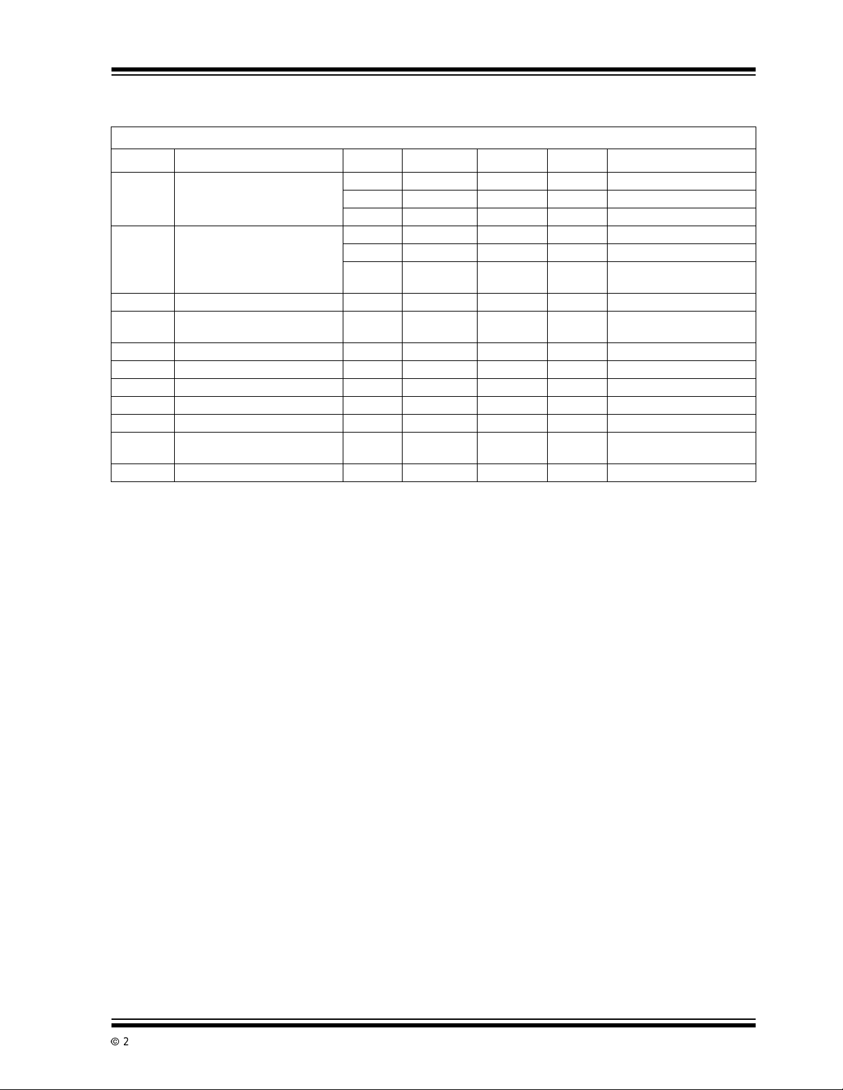
Device Selection Table
Part
Number
TC820CPL 3-3/4 Digits 40-Pin PDIP 0°Cto+70°C
TC820CKW 3-3/4Digits 44-PinPQFP 0°Cto+70°C
TC820CLW 3-3/4 Digits 44-Pin PLCC 0°Cto+70°C
2002 Microchip TechnologyInc. DS21476B-page 1
Resolution Package
Operating
Temp. Range
Page 2

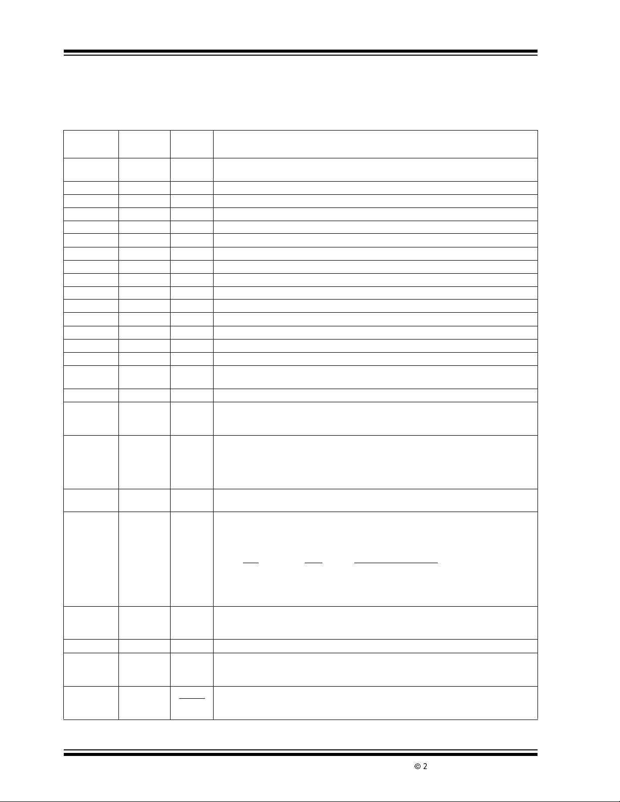
TC820
S
Package Type
44-Pin PLCC
BC3P2
OFE2
AGD2
BC2P1
PKFE1
AGD1
BP1BT
BP3
BP2
BP1
V
DISP
BC3P2
OFE2
AGD2
BC2P1
PKFE1
AGD1
BC1BT
BP3
BP2
BP1
V
DISP
AGD3
HFE3
BC4P3
6543 1442
7
8
9
10
11
12
13
14
15
16
17
18 19 20 21 23 24
DGND
AGD4
TC820CLW
LOGIC
ANNUNC
RANGE/FREQ
44-Pin PQFP
AGD3
BC4P3
HFE3
44 43 42 41 39 3840
1
2
3
4
5
6
7
8
9
10
11
12 13 14 15 17 18
DGND
AGD4
TC820CKW
LOGIC
ANNUNC
RANGE/FREQ
22
L–E4
16
DP0/LO
DD
L-E4
V
DP1/HI
DP0/LO
DD
V
DP1/HI
OSC3
OSC242OSC141EOC/HOLD
43
25
26
BUZIN
BUZOUT
FREQ/VOLTS
OSC1
OSC3
OSC2
37 36 35 34
19
20
21 22
BUZIN
BUZOUT
FREQ/VOLTS
INT
V
40
27 28
UR
PKHOLD
INT
V
EOC/HOLD
33
32
31
30
29
28
27
26
25
24
23
UR
PKHOLD
39
38
37
36
35
34
33
32
31
30
29
C
V
VIN+
V
V
V
C
C
COM
V
OR
C
AZ
V
BUFF
VIN+
V
IN
V
REF
V
REF
C
REF
C
REF
COM
V
SS
OR
AZ
BUFF
-
IN
REF
REF
REF
REF
SS
-
-
+
-
+
-
+
-
+
Segments L-E4
Segments AGD4
Segments BC4P3
Segments HFE3
Segments AGD3
Segments BC3P2
Segments OFE2
Segments AGD2
Segments BC2P1
Segments PKFE1
Segments AGD1
Segments BC1BT
BP3
BP2
BP1
DGND
ANNUNC
LOGIC
RANGE/FREQ
DP0/LO
40-Pin PDIP
1
2
3
4
5
6
7
8
9
TC820CPL
10
11
12
13
14
15
16
17
18
19
20
V
40
DD
OSC3
39
38
OSC2
OSC1
37
V
36
INT
C
35
AZ
V
34
BUFF
+
V
33
IN
-
V
32
IN
-
V
31
REF
+
V
30
REF
C
29
28
27
26
25
24
23
22
21
-
REF
+
C
REF
COM
V
SS
PKHOLD
FREQ/VOLT
BUZIN
BUZOUT
DP1/HI
DS21476B-page 2
2002 Microchip TechnologyInc.
Page 3

Typical Applications
/
TC820
Triplex LCD
EOC
Under Range
Over Range
Analog Input
Full Scale Select
Frequency Input
Logic Probe
Input
Low Drift Voltage
Differential
Reference
3-3/4 Digit A/D
Converter
Analog GND
Auto-Ranging
Frequency
Counter
Logic Probe
Digital Ground
Logic High
Logic Low
To LCD
and Buzzer
Over Range PKHold Low Batt
Clock
Oscillator
TC820
Peak Hold
Comparator
Peak
Hold
Triple LCD
Drivers
Low
Battery
Detect
+
9V
Annunciator Drive
Decimal
Point
Drivers
Buzzer
Driver
Function
Select
Volts
Frequency
Logic
Buzzer
Control
Decimal
Point
Select
Function
Select
C
REF
VIN+
VIN-
V
REF
V
REF
Common
V
DD
V
SS
+C
+
-
REF-VBUFF
DGND
C
Detect
UR OR
AZ
Low
Batt
V
INT
To LCD
A/D Control
DEINT
Under Range
Over Range
Range Frequency
Range
Input
EOC/
HOLD
EOC
÷2
TC820
PEAK
HOLD
OSC3OSC2OSC1
Logic
Low
Frequency Counter Input
A/D Counter Select
SEL
B
A
Low Batt
ANNUNC
V
÷8
DISP
BUZIN
Range
A/D Counter
(3999 Counts)
Comparator
A > B
Display
Latch
Logic
Triples
Drivers
SEG0 • • • BP3
Low
Buzzer
Driver
Range/
Frequency
Frequency
Volts
Logic
DP0/LO
15
DP1/HI
2002 Microchip TechnologyInc. DS21476B-page 3
Page 4

TC820
1.0 ELECTRICAL
CHARACTERISTICS
Absolute Maximum Ratings*
Supply Voltage (VDDto GND) ................................15V
*Stresses above those listed under "Absolute Maximum
Ratings" may cause permanent damage to the device. These
are stress ratings only and functional operation of the device
at these or any other conditions above those indicated in the
operation sections of the specifications is not implied.
Exposure to Absolute Maximum Rating conditions for
extended periods may affectdevice reliability.
Analog Input Voltage:
(Either Input) (Note 1) ............................ V
Reference Input Voltage(Either Input)....... VDDto V
DD
to V
SS
SS
Digital Inputs...........................................VDDto DGND
....................................... VDDto (DGND – 0.3V)
V
DISP
Package Power Dissipation (T
–70°C)(Note 2):
A
40-Pin Plastic DIP ......................................... 1.23W
44-Pin PLCC ..................................................1.23W
44-Pin Plastic Flat Package (PQFP) ..............1.00W
Operating Temperature Range:
"C" Devices ......................................... 0°C to +70°C
"E" Devices.......................................-40°C to +85°C
StorageTemperature Range..............-65°C to +150°C
TC820 ELECTRICAL SPECIFICATIONS
Electrical Characteristics: VS=9V,TA= 25°C, unless otherwise specified.
Symbol Parameter Min Typ Max Units Test Conditions
Zero Input Reading -000 ±000 +000 Digital
Reading
RE Rollover Error -1 ±0.2 +1 Counts V
NL Nonlinearity
(Maximum Deviation From Best
Straight Line Fit)
Ratiometric Reading 1999 1999/2000 2000 — V
CMRR Common Mode Rejection Ratio — 50 — µV/V V
VCMR Common Mode Voltage Range V
e
N
I
IN
V
COM
V
CTC
Note 1: Inputvoltages may exceedthesupply voltages providedthat input currentis limited to ±100µA.Currentabove this value
Noise (P-P Value Not
Exceeded95% of Time)
Input LeakageCurrent — — — — VIN=0V
AnalogCommonVoltage 3.15 3.3 3.45 V 25kΩ between Common and
Common Voltage Temperature
Coefficient
may result in invaliddisplay readings,butwillnotdestroy the deviceif limitedt o ±1mA.
2: Dissipation ratings assumedevice is mounted with all leads solderedto printed circuit board.
-1 ±0.2 +1 Count Full Scale = 400mV
+1.5 — VDD– 1 Input High, Input Low
SS
—15 —µVVIN=0V
—1 10pAT
—20 —pA0°C≤ T
—100 —pA-40°C≤ T
—— ——25kΩ BetweenCommon and
—35 50ppm/°C0°C≤ TA≤ +70°C
—50 ——-40°C≤ T
=0V
V
IN
Full Scale= 400mV
= ±390mV
IN
Full Scale= 400mV
IN=VREF
CM
Full Scale= 400mV
(V
FS
Full Scale= 400mV
A
V
DD(VSS-VCOM
V
DD
,TC820
=±1V,VIN=0V
=200mV)
=25°C
≤ +70°C
A
≤ +85°C
A
≤ +85°C
A
)
DS21476B-page 4
2002 Microchip TechnologyInc.
Page 5
TC820
TC820 ELECTRICAL SPECIFICATIONS (CONTINUED)
Electrical Characteristics: VS=9V,TA= 25°C, unless otherwise specified.
Symbol Parameter Min Typ Max Units Test Conditions
TC
ZS
TC
FS
I
S
V
IL
V
IH
V
OL
Note 1: Inputvoltages may exceedthesupply voltages providedthat input current is limitedto±100µA. Current above thisvalue
Zero Reading Drift — — — — VIN=0V
—0.2 ——0°C≤ T
—1 ——-40°C≤ T
Scale Factor Temperature
Coefficient
—— ——V
—1 5ppm/°C0°C≤ T
— 5 — ppm/°C -40°C ≤ T
Supply Current — 1 1.5 mA VIN=0V
Peak-to-Peak Backplane
4.25 4.7 5.3 V V
Drive Voltage
Buzzer Frequency — 5 — kHz F
Counter TIme-Base Period — 1 — Second F
Low Battery Flag Voltage 6.7 7 7.3 V V
Input Low Voltage — — DGND + 1.5 V
Input High Voltage VDD–1.5 — — V
Output Low Voltage,
VDD–1.5 — DGND+0.4 V IL=50µA
UR, OR Outputs
Control Pin Pull-down Current — 5 — µAV
may result in invaliddisplay readings,butwillnotdestroy the deviceif limitedt o ±1mA.
2: Dissipation ratings assumedevice is mounted with all leads solderedto printed circuit board.
≤ +70°C
A
≤ +85°C
A
=399mV
IN
≤ +70°C
A
≤ +85°C
=9V
S
=DGND
DISP
=40kHz
OSC
=40kHz
OSC
to V
DD
IN=VDD
A
SS
Ext Ref = 0ppm/°C
V
2002 Microchip TechnologyInc. DS21476B-page 5
Page 6
TC820
2.0 PIN DESCRIPTIONS
ThedescriptionsofthepinsarelistedinTable2-1.
TABLE 2-1: PIN F UNCTION TABLE
Pin Number
(40-PDIP)
1 40 L-E4 LCD segment driver for L ("logic LOW"), polarity, and "e" segment of most significant
2 41 AGD4 LCD segment drive for "a," "g," and "d" segments of MSD.
3 42 BC4P3 LCD segmentdrivefor "b" and "c" segmentsof MSD and decimal point 3.
4 43 HFE3 LCD segment drive for H ("logic HIGH"), and "f" and "e" segmentsof third LSD.
5 44 AGD3 LCD segment drive for "a," "g," and "d" segments of third LSD.
6 1 BC3P2 LCD segmentdrive for "b" and "c" segmentsof third LSD and decimal point 2.
7 2 OFE2 LCD segmentdrive for "over range," and "f" and "e" segments of second LSD.
8 3 AGD2 LCD segment drive for "a," "g," and "d" segmentsof second LSD.
9 4 BC2P1 LCD segmentdrivefor "b " and "c" segmentsof second LSD and decimal point 1.
10 5 PKFE1 LCD segment drive for "hold peak reading," and "f" and "e" segmentsof LSD.
11 6 AGD1 LCD segment drive for "a," "g," and "d" segments of LSD.
12 7 BC1BT LCD segmentdrivefor"b"and "c" segments of LSD and "low battery."
13 8 BP3 LCD backplane#3.
14 9 BP2 LCD backplane#2.
15 10 BP1 LCD backplane#1.
—11V
16 12 DGND Internal logicdigital ground,thelogic "0" level. Nominally4.7VbelowV
17 13 ANNUNC Square-wave output at the backplane frequency, synchronized t o BP1. ANNUNC can be
18 14 LOGIC Logic mode control input. When connected to V
19 15 RANGE/
20 16 DP0/LO D ual purpose input. Decimalpoint select input for voltagemeasurements. In logic mode,
Pin Number
(44-PQFP)
Symbol Description
digit (MSD).
DISP
FREQ
Sets peak LCD drive signal: V
compensate for temperature variation of LCD crystal threshold voltage.
used to control display annunciators. Connecting an LCD segment to ANNUNC turns it
on; connecting it to its backplane turns it off.
LCD displays "OL"andthedecimal pointinputs controlthe HIGH and LOWannunciators.
When the "low" annunciator is on, the buzzer will also be on. When unconnectedor connected to DGND, the TC820 is in the Voltage/FrequencyMeasurementmode.Thispin
has a 5µA internal pull-down to DGND
Dual purposeinput. In Rangemode,whenconnected to VDD, the integration time
will be 200 counts instead of 2000 counts
connecting this pin to V
pull-down to DGND in Volts mode only. Decimalpoint logic:
willturn on the "low" LCD segment. Thereis an internal5µA
DD
PEAK
=(VDD)–V
.
DISP.VDISP
DD
mayalsobeusedto
DD
, the converteris in Logic mode. The
.
DP1
00 None
01 DP1
10 DP2
11 DP3
21 17 DP1/HI Dual purpose input. Decimalpoint selectinput for voltagemeasurements. In Logic mode,
22 18 BUZOUT Buzzer output. Audio frequency, 5kHz, output which drives a piezoelectric buzzer.
23 19 BUZIN Buzzercontrol input.Connecting BUZIN to V
24 20 FREQ/
VOLTS
DS21476B-page 6
connecting this pin to V
pull-down to DGND in Volts mode only.
OR’ed (internally)withthe "logiclevel low" input. There is an internal 5µApull-downto
DGND.
Voltage or frequencymeasurement selectinput. When unconnected,or connected
VOLTS to DGND, the A/D converter function is active. When connected to V
frequency counter function is active. This pin has an internal 5µA pull-down to DGND.
DPQ Decimal Point Selected
will turn on the "high" LCD segment. There is an internal 5µA
DD
turns the buzzer on. BUZIN is logically
DD
2002 Microchip TechnologyInc.
DD
,the
Page 7
TC820
TABLE 2-1: PIN FUNCTION TABLE (CONTINUED)
Pin Number
(40-PDIP)
25 21 PKHOLD Peak hold input. When connectedto VDD, the converter will only update the display if a
— 22 UR Under range output.Thisoutputwill be HIGH when the digitalreading is 380
— 23 OR Over range output. This output will be HIGH when the analog signal inputis greater
26 24 V
27 25 COM Analog circuit ground reference point. Nominally 3.3V below V
28 26 C
29 27 C
30 28 V
31 29 V
32 30 V
33 31 V
34 32 V
35 33 C
36 34 V
—35EOC
37 36 OSC1 Crystal oscillator (input)connection.
38 37 OSC2 Crystal oscillator (output) connection.
39 38 OSC3 RC oscillator connection.
40 39 V
Pin Number
(44-PQFP)
Symbol Description
new conversion value is greaterthanthepreceding value.Thus,thepeakreading will be
storedand held indefinitely. When unconnected, or connected to DGND, the converter
will operate normally. This pin has an internal 5µA pull-down to DGND.
countsor less.
than full scale. The LCD will display"OL"whenthe inputis over ranged.
Negative supply connection. Connect to negativeterminal of 9V battery.
SS
+ P ositive connection for referencecapacitor.
REF
- Negative connection for reference capacitor.
REF
+ High differential reference input connection.
REF
- Low differential reference input connection.
REF
- Low analog input signal connection.
IN
+ High analoginput signalconnection.
IN
Buffer output. Connect to integration resistor.
BUFF
Auto-zero capacitor connection.
AZ
Integrator output. Connect to integration capacitor.
INT
/
Bi-directionalpin. Pulses low (i.e., from VDDto DGND) at the end of each conversion. If
HOLD
connected to V
LCD segmentdrive for "a," "g,"and "d" segmentsof MSD.
DD
, conversions will continue,butthe displayisnot updated.
DD
DD
.
2002 Microchip TechnologyInc. DS21476B-page 7
Page 8
TC820
3.0 DETAILED DESCRIPTION
The TC820 is a 3-3/4 digit measurement system combining an integrating analog-to-digital converter, frequency counter, and logic level tester in a single
package. The TC820 supersedes the TC7106 in new
designs by improving performance and reducing system cost. The TC820 adds features that are difficult,
expensive,orimpossibleto provide with olderA/D converters (see Table 3-1). The high level of integration
permitsTC820basedinstruments to deliver higher performance and more f eatures, while actually reducing
partscount.Fabricated in low power CMOS, the TC820
directly drives a 3-3/4 digit (3999 maximum) LCD.
With a maximum range of 3999 counts,the TC820 provides 10 times greater resolution in the 200mV to
400mV range than traditional 3-1/2 digit meters. An
auto-zerocycleensuresazero reading with a 0V input.
CMOS processing reduces analog input biascurrent to
only 1pA. Rollover error (the difference in readings for
equal magnitude but opposite polarity input signals) is
less than ±1 count. Differential reference inputs permit
ratiometric measurements for ohms or bridge transducer applications.
The TC820's frequency counter option simplifies
design of an instrument well-suited to both analog and
digitaltroubleshooting: voltage,current,and resistance
measurements, plus precise frequency measurements
to 4MHz ( higher frequencies can be measured with an
external pr escaler), and a simple logic probe. The frequency counter will automatically adjust its range to
match the input frequency, over a four-decade range.
Two logic level measurement inputs permit a TC820
based meter to function as a logic probe. When combinedwithexternallevel shifters,theTC820willdisplay
logiclevelson the LCD and also turn on a piezoelectric
buzzer when the measured l ogic level is low.
Other TC820 features simplify instrument design and
reduce parts count. On-chip decimal point dr ivers are
included, as is a low battery detection annunciator. A
piezoelectricbuzzer can be controlled with an external
switch or by the logic probe inputs. Two oscillator
optionsareprovided: a crystalcanbeusedifhighaccuracy frequency measurements are desired, or a simple
RC option can be used for low-end instruments.
A "peak reading hold" input allows the TC820 to retain
the highest A/D or frequency reading. This feature is
useful in measuring motor starting current, maximum
temperature, and similar applications.
A family of instruments can be created with the TC820.
No additional design effort is required to create instruments with 3-3/4 digit resolution.
The TC820 operates from a single 9V battery, with typical power of 10mW.Packages include a 40-pin plastic
DIP, 44- pin plastic flat package (PQFP), and 44-pin
PLCC.
TABLE 3-1: COMPETITIVE EVALUATION
Features Comparison TC820 7106
3-3/4 Digit Resolution Yes No
Auto-Ranging Frequency
Counter
Logic Probe Yes No
Decimal Point Drive Yes No
Peak Reading Hold
(Frequency or Voltage)
Display Hold Yes No
Simple10:1RangeChange Yes No
Buzzer Drive Yes No
Low Battery Detection
withAnnunciator
Over Range Detection
withAnnunciator
Low Drift Reference Y e s No
Under Range/Over Range
Logic Output
Input Overload Display "OL" "1"
LCD Annunciator Driver Yes No
LCD Drive Type Triplexed Direct
LCD Pin Connections 15 24
LCD Elements 36 23
Yes No
Yes No
Yes No
Yes No
Yes No
3.1 General Theory of Operation
3.1.1 DUAL SLOPE CONVER SION
PRINCIPLES
The TC820 analog-to-digital converter operates on t he
principle of dual slope integration. An understanding of
the dual slope conversion technique will aid the user in
followingthedetailedTC820theoryof operationfollowing this section. A conventional dual slope converter
measurement cycle has t wo distinct phases:
1. Input Signal Integration
2. Reference Voltage Integration (De-integration)
Referring to Figure 3-1, the unknown input signal to be
convertedisintegratedfromzerofora fixedtimeperiod
(t
), measured by counting clock pulses. A constant
INT
reference voltage of the opposite polarity is then integrated until the integrator output voltage returns to
zero. The reference integration (de-integration) time
(t
) is then directly proportional to the unknown
DEINT
input voltage (V
).
IN
DS21476B-page 8
2002 Microchip TechnologyInc.
Page 9

TC820
g
T
In a simple dual slope converter, a complete conversion requires the integrator output to "ramp-up" from
zero and "ramp-down" back to zero. A simple mathematicalequationrelates the inputsignal,referencevoltage, and integration time.
EQUATION 3-1:
1
R
INTCINT
Where: V
REF
t
INT
t
DEINT
For a constant V
t
INT
V
IN
∫
0
= Ref erence Voltage
= I ntegration Time
= De- integration Time
:
INT
(t)dt =
V
REFtDEINT
R
INTCINT
EQUATION 3-2:
t
REF
DEINT
t
INT
VIN=V
FIGURE 3-1: BASIC DUAL SLOPE
CONVERTER
Analog
Input Signal
REF
Voltage
Output
Integrator
Fixed Signal
Integrate Time
R
Polarity Control
Accuracy in a dual slope converter is unrelated to the
integrating resistor and capacitor values as long as
they are stable during a measurement cycle. An inherent benefit of the dual slope technique is noise immunity. Noise spikes are integrated or averaged to zero
during the integration periods, making integrating
ADCs immune to the large conversion errors that
plague successive approximation converters in high
noise environments. Interfering signals, with frequency
components at multiples of the averaging (integrating)
period, will be attenuated (Figure 3-2). Integrating
ADCs commonly operate with the signal integration
period set to a multiple of the 50/60Hz power line
period.
C
Integrator
–
+
Switch
Driver
Phase
Control
Display
V
= V
IN
VIN = 1.2V
Variable Reference
Inte
rate Time
Comparator
–
+
Control
Logioc
REF
REF
Clock
Counter
FIGURE 3-2: NORMAL MODE
REJECTION O F DUAL
SLOPE CONVERTER
30
T = Measurement
Period
20
10
Normal Mode Rejection (dB)
0
0.1/T 1/T 10/
Input Frequency
3.2 Analog Section
In addition to the basic integrate and de-integrate dual
slope phases discussed above, the TC820 design
incorporates a "zero integrator output" phase and an
"auto-zero" phase. These additional phases ensure
thatthe integratorstartsat0V(evenaftera severe over
range conversion), and that all offset voltage errors
(buffer amplifier, integrator and comparator) are
removed f rom t he conversion. A true digital zero reading is assured without any external adjustments.
A complete conversion consists of four distinctphases:
1. Zero IntegratorOutput
2. Auto-Zero
3. Signal Integrate
4. Reference De-integrate
3.2.1 ZE RO INTEGRATOR OUTPUT
PHASE
This phase guarantees that the integrator output is at
0V before the system zero phase is entered, ensuring
that the true system offset voltages will be compensated for even after an over range conversion. The
duration of this phase is 500 counts plus the unused
de-integrate counts.
3.2.2 AUTO-ZERO PHASE
During the auto-zero phase, the differentialinputsignal
is disconnectedfrom the measurement circuit by opening internalanalogswitches,andthe internalnodesare
shortedtoAnalogCommon(0V
input condition. Additional analog switches close a
feedback loop around the integrator and comparator to
permitcomparatoroffset voltageerrorcompensation.A
voltageestablishedon C
then compensatesforinter-
AZ
nal device offset voltages during the m easurement
cycle.The auto-zerophaseresidualis typically10µVto
15µV. The auto-zero duration is 1500 counts.
)toestablishazero
REF
2002 Microchip TechnologyInc. DS21476B-page 9
Page 10

TC820
3.2.3 SIGNAL INTEGRATION PHASE
Upon completion of the auto-zero phase, the auto-zero
loop is opened and the internal differential inputs c onnect to V
+ and VIN-. The differential input signal is
IN
then integrated for a fixed time period, which is 2000
counts (4000 clock periods). The externally set clock
frequencyis divided by two before clocking the internal
counters.
The i ntegration t ime period is:
EQUATION 3-3:
4000
t
=
INT
F
OSC
The differential input voltage must be within t he
device's Common mode range when the converter and
measured system share the same power supply common (ground). If the converter and measured system
do not share the same power supply common, as in
battery powered applications, V
-shouldbetiedto
IN
analog common.
Polarity is determined at the end of signal integration
phase. The sign bit i s a "true polarity" indication, in that
signals less than 1LSB are correctly determined. This
allows precision null detection that is limited only by
device noise and auto-zero residual offsets.
3.2.4 REFERENCE INTEGRATE
(DE-INTEGRATE) PHASE
The reference capacitor,which was charged during the
auto-zero phase, is connected t o the input of the integrating amplifier. The internal sign logic ensures the
polarityof the reference voltageis always connected in
the phase opposite to that of the input voltage. This
causestheintegrator to ramp back to zero at a constant
rate, determined by the reference potential.
The amount of time required (t
) for the integrating
DEINT
amplifier to reach zero is directly proportional to the
amplitudeof the voltage that was put on the i ntegrating
capacitor(V
) during the integration phase.
INT
EQUATION 3-4:
R
t
DEINT
The digital reading displayed by the TC820 is:
Digital Count = 2000
INTCINTVINT
=
V
REF
VIN+VIN-
V
REF
The oscillator frequency is divided by 2 prior to clocking the internal decade counters. The four-phase measurement cycle takes a total of 8000 (4000) counts or
16,000clockpulses.The8000 count phaseis independent of input signal magnitude or polarity.
Each phase of the measurement cycle has the following length:
TABLE 3-2: MEASUREMENT CYCLE
PHASE LENGTH
Conversion Phase Counts
1) Auto-Zero 1500
2) Signal Integrate (Notes 1, 2) 2000
3) Reference Integrate 1 to 4001
4) IntegratorOutput Zero 499 to 4499
Note 1: This time period is fixed. The integration period for
theTC820 is:
t
(TC820) = 4000/F
INT
Where F
2: Times shown are the RANGE/FREQ at logic low (normal
operation). When RANGE/FREQ is logic high, signal
integrate times are 200 counts. See Section 3.2.7,
“10:1 Range Change”.
is the clock oscillator frequency.
OSC
= 2000 counts.
OSC
3.2.5 INPUT OVER RANGE
When the analog i nput is greater than full scale, the
LCD will di splay "OL" and the "OVER RANGE" LCD
annunciator will be on.
3.2.6 PEAK READING HOLD
The TC820 provides the capability of holding the highest (or peak) reading. Connecting the PK HOLD input
to V
each conversion, the contents of the TC820 counter
are compared to the contents of the display register. If
the new reading is higher than the reading being displayed, the higher reading is transferred to the display
register. A "higher" reading is defined as the reading
with the higher absolute value.
The peak reading is held in the display register, so the
reading will not "droop" or slowly decay with time. The
held reading will be retained until a higher r eading
occurs, the PK HOLD input is disconnected from V
or power is removed.
The peak signal to be measured must be present during the TC820 signalintegrateperiod.TheTC820 does
not performtransientpeak detectionoftheanaloginput
signal. However, in many cases, such as measuring
temperature or electric motor starting current, the
TC820 "acquisition time" will not be a limitation. If true
peak detection is required, a simple circuit will suffice.
See t he applications section for details.
The peak reading function is also available when the
TC820 is in the Frequency Counter mode. The counter
auto-ranging feature is disabled when peak reading
hold is selected.
enables the peak hold feature. At t he end of
DD
DD
,
DS21476B-page 10
2002 Microchip TechnologyInc.
Page 11

TC820
3.2.7 10:1 RANGE CHANGE
The analog input f ull scale range can be changed with
the RANGE/FREQ input. Normally, RANGE/FREQ is
held low by an internal pull-down. Connecting this pin
to V
+ will increase the full scale voltage by a factor
S
of 10. No externalcomponent changes are required.
The RANG E/FREQ input operates by changing the
integrate period. When RANGE/FREQ is connected to
V
, the signal integration phase of the conversion is
DD
reduced by a factor of 10 (i.e.,from 2000 countsto 200
counts).
For the TC820, the 10:1range change will result in ±4V
full scale.Thisfullscalerangewill exceed the Common
mode range of the input buffer when operating f rom a
9V battery.Ifrange changing is required for the TC820,
a higher supply voltage can be provided, or t he input
voltage can be divided by 2 externally.
3.3 Frequency Counter
In addition to serving as an analog-to-digital converter,
the TC820 internal counter can also function as a frequency counter (Figure 3-3). In the Counter mode,
pulses at the RANGE/FREQ input will be counted and
displayed.
The frequency counter derives its time-base from the
clock oscillator.The counter time-base is:
EQUATION 3-5:
F
t
COUNT
=
OSC
40,000
Thus, the counter will operate with a 1-second timebase when a 40kHz oscillator is used. The frequency
counter accuracy is determined by the oscillator accuracy. For accurate frequency measurements, a crystal
oscillatoris recommended.
The frequency counter will automatically select the
proper range. Auto-range operation extends over four
decades, from 3.999kHz to 3.999MHz. Decimal points
are set automaticallyinthe Frequency mode (Figure 3-4).
The logic switching levels of the RANGE/FREQ input
are CMOS levels.For best counter operation, an external buffer is recommended. See the applications section for details.
3.4 Logic Probe
The TC820 can also function as a simple logic probe
(Figure3-5). This mode is selected when the LOGIC
input is high. Two dual purpose pins, which normally
control the decimal points, are used as logic inputs.
Connecting either input to a logic high level will turn on
the corresponding LCD annunciator. When the "low"
annunciatoris on, the buzzer will be on. As with the frequency counter input, external level shifters/buffers are
recommended for the logic probe inputs.
FIGURE 3-3: TC820 COUNTER OPERATION
TC820
From Integrator
of A/D Converter
FREQ/
VOLTS
RANGE/
FREQ
Clock
Oscillator
A/D Converter/Frequency
Counter Select
Frequency Input
÷2
÷20,000
Frequency Counter
Programmable
Divider
( ÷1, 10, 100, 1000)
A/D Converter
Comparator
To Decimal
Point Drivers
Auto-Range
Control
LCD
Data Latch, Peak Hold
Register, LCD
Decoder/Drivers
Enable
3-3/4 Digit Counter
Count Overflow
Under Range
Control
Over Range
Detect
2002 Microchip TechnologyInc. DS21476B-page 11
Page 12

TC820
FIGURE 3-4: AUTO-RANGE DECIMAL POINT SELECTION V S . FREQUENCY COUNTER INPUT
DP3 DP2 DP1
f
IN
0Hz - 3999Hz
4kHz - 39.99kHz
40kHz - 399.9kHz
400kHz
FIGURE 3-5: LOGIC PROBE SIMPLIFIED SCHEMATIC
Decimal Point
DP3
DP2
DP1
NONE
LCD
High
Low
and Pulse Stretching
Logic
Probe
Input
External Logic
Level Detection
CMOS
Logic Levels
V
DD
TC820
DP0/LO
DP1/HI
LOGIC
LCD
Drivers
NC
Disable A/D Converter
To Buzzer
DS21476B-page 12
2002 Microchip TechnologyInc.
Page 13

TC820
g
When the logic probe function is selected while FREQ/
VOLTS
is low (A/D mode), the ADC will remain in the
Auto-Zero mode. The L CD will read "OL" and all
decimal points will be off (Figure 3-6).
FIGURE 3-6:
*
High
**
Low
* "High" Annuciator will be on when DP1/HI = Logic High
** "Low" Annunciator and Buzzer will be on when DP0/LO = Lo
ic High
If the logic probe is active while FREQ/VOLTS is high
(Counter mode), the f requency counter will continue to
operate. The display will read "OL" but the decimal
pointswillbe visible. If the logicprobeinput is also connected to the RANGE/FREQ input, bringing the LOGIC
input low will immediately display the frequency at t he
logic probe input.
3.5 Analog Pin Functional Description
3.5.1 DIFFERENTIAL SIGNAL INPUTS
(V
+), (VIN-)
IN
The TC820 is designed withtrue differentialinputs, and
accepts input signals within the Input Stage Common
mode voltage (V
V
–1VtoVSS+ 1.5V. Common mode voltages are
DD
removed from the system when the TC820 operates
from a battery or floating power source (isolated from
measured system) and V
common(seeFigure3-7).
In systems where Common mode voltages exist, the
86dB Common mode rejection ratio minimizes error.
Common mode voltages do, however, affect the integrator output level. A worst case condition exists if a
large, positive V
scale, negative differential signal. The negative signal
drives the integrator output positive along with V
(Figure 3-8). For such applications, the integrator output swing can be reduced below the recommended 2V
full scale swing. The integrator output will swing within
0.3V of V
,orVDDwithout increased linearity error.
DD
3.5.2 REFERENCE (VDD,VSS)
The TC820 r eference, like the analog signal input, has
true differential inputs. In addition, the reference voltage can be generated anywhere within the power supply voltage of the converter. The differential reference
inputs permit ratiometric measurements and simplify
interfacingwith sensors, suchasloadcellsandtemperature sensors.
) r ange. The typical range is
CM
is connected to analog
SS
exists in conjunction with a full
CM
CM
To prevent rollover type errors from being induced by
large Common mode voltages, C
should be large
REF
comparedtostraynodecapacitance.A0.1µFcapacitor
is typical.
The TC820 offers a significantly improved analog common temperature coefficient, providing a very stable
voltage suitable for use as a voltage reference. The
temperature coefficient of analog common i s typically
35ppm/°C.
3.5.3 ANALOG COMMON
The analog common pin is set at a voltage potential
approximately 3.3V below V
between 3.15V and 3. 45V below V
is tied internally to an N-channel FET capable of sinking 3mA. This FET will hold the common line at 3. 3V
below V
commonlinetowardV
should an external load attempt to pull the
DD
. Analog common source cur-
DD
rent is limited to 12µA, and is, therefore,easilypulledto
a more negative voltage (i.e., below V
The TC820 connects the internal V
to analog common during the auto-zero cycle. During
the reference integrate phase, V
analog common. If V
- is not externally connected to
IN
analog common, a Common mode voltage exists.
Thisisrejectedbytheconverter's86dBCommonmode
rejection ratio. In battery powered applications, analog
common and V
- are usually connected, removing
IN
Common mode voltage concerns. In systems wher e
V
- is connected to the power supply ground or to a
IN
given voltage, analog common should be connected to
V
-.
IN
The analog common pin serves to set t he analog section reference or common point. The TC820 is specifically designed to operate from a battery, or in any
“measurement"systemwhere input signals are not referenced (float), with respect to the TC820 power
source. The analog common potential of V
gives a 7V end of battery life voltage. The analog common potential has a voltage coefficient of 0.001%.
With a sufficiently high total supply voltage
(V
DD–VSS
> 7V) , analog common is a v ery stable
potential with excellent temperature stability (typically
35ppm/°C). This potential can be used to generate the
TC820 reference voltage. An external voltage reference will be unnecessary in most cases, because of
the 35ppm/°Ctemperaturecoefficient. See the applications section for details.
. This potential is
DD
. Analog common
DD
–3.3V).
DD
+ and VIN- inputs
IN
- is connected to
IN
DD
–3.3V
2002 Microchip TechnologyInc. DS21476B-page 13
Page 14

TC820
FIGURE 3-7: COMMON MODE VOLTAGE REMOVE D IN BATTERY OPERATION WITH
V
= ANALOG COMMON
IN
V+ V-
Power
Source
Measured
System
V+
V-
GND
GND
V
BUF
+
V
IN
V
-
IN
Analog
Common
C
V
AZ
REF
V
INT
TC820
V
-
REF
Segment
Drive
+
V
DD
+
9V
BP1
V
SS
BP2
OSC1
OSC2
OSC3
LCD
BP3
NC
FIGURE 3-8: COMMON MODE VOLTAGE REDUCES AVAILABLE INT EGRATOR SWING
COM
≠ VIN)
+
Input Buffer
+
C
I
R
I
(V
–
V
IN
+
Integrator
–
V
I
–
T
I
VI =
V
CM
Where:
T
= Integration Time =
I
= Integration Capacitor
C
I
= Integration Resistor
R
I
RI C
VCM – V
[
I
IN
[
4000
F
OSC
DS21476B-page 14
2002 Microchip TechnologyInc.
Page 15

TC820
4.0 FUNCTION CONTROL INPUTS
PIN
4.1 Functional D escription
The TC820 Operating modes are selected with the
function control inputs. See the control input truth,
Table 4-1. The high logic threshold is ≥ V
the low logic level is ≤ DGND +1.5V.
TABLE 4-1: T C820 CONTROL INPUT
TRUTH TABLE
Logic Input
FREQ/
VOLTS
Note 1: Logic "0" = DGND
RANGE/
FREQ
X X 1 LogicProbe
0 0 0 A/D Converter,
0 1 0 A/D Converter,
1 Frequency
Counter
Input
2: Logic "1" = V
LOGIC
0 Frequency Counter
-
DD
TC820 Function
V
FULL SCALE
V
FULL SCALE
4.1.1 FREQ/VOLTS
This input determineswhetherthe TC820 is in the Analog-to-Digital Conversion mode, or in the Frequency
Counter mode. When FREQ/VOLTS
V
, the TC820 willmeasurefrequencyatthe RANGE/
DD
FREQ input. When unconnected, or connected to
DGND, the TC820 wi ll operate as an analog-to-digital
converter. This input has an internal 5µA pull-down to
DGND.
–1.5Vand
DD
=2xV
REF
=20xV
REF
is connected to
When the TC820 analog-to-digitalconverter function is
selected, connecting RANGE/FREQ to V
will divide
DD
the integration time by 10. Therefore, the RANGE/
FREQ input can be used to perform a 10:1 range
change without changing external components.
4.1.4 DP0/LO, DP1 /HI
The function of these dual purpose pins is determined
by the LOGIC input. W hen the TC820 is in the Analogto-Digital Converter mode, these inputs control the
LCD decimal points. See the decimal point truth,
Table 4-2. These inputs have internal 5µA pull-downs
to DGND when the Voltage/Frequency Measurement
mode i s active.
TABLE 4-2: TC820 DECIMAL POINT
TRUTH TABLE
DP1 DP0 LCD
0 0 3999
0 1 399.9
10 39.99
11 3.999
Connecting the L OGIC input to V
in the Logic Probe mode. In thismode,theDP0/LO and
DP1/HI inputs control the LCD "low" and "high" annunciators directly. When DP1/HI is connected to V
"high" annunciator will turn on. When DP0/LO is connectedtoV
, the "low" annunciator and the buzzer
DD
will turn on. The internal pull-downs on these pins ar e
disabled when the logic probe function is selected.
These inputs have CMOS logic switching thresholds.
For optimum per formance as a logic probe, external
level shifters are recommended. See the applications
section for details.
places the TC820
DD
DD
,the
4.1.2 LOGIC
The LOGIC input is used to activate the logic probe
function.When connected to V
the Logic Probe mode. The LCD will show "OL" and all
decimal points will be off. The decimal point inputs
directly control "high" and "low" display annunciators.
When LOGIC is unconnected, or connected to DGND,
the TC820 will perform analog-to-digital or frequency
, the TC820 will enter
DD
4.1.5 BUZIN
This input controls the TC820 on-chip buzzer driver.
Connecting BUZIN to V
will turn the buzzer on.
DD
Thereis an external pull-downto DGND. BUZIN can be
used with external circuitry to provide additional functions, such as a fast, audible continuity indication.
4.2 Additional Features
measurements, as selected by the FREQ/VOLTS
input. The LOGIC input has an internal 5µA pull-down
to DGND.
The TC820 is available in 40-pin and 44-pin packages.
Several additional features are available in the 44-pin
package.
4.1.3 RANGE/FREQ
The function of this dual purpose pin is determined by
the FREQ/VOLTS
nectedtoV
DD
quency counter function. Pulses at this input are
counted with a time-base equal to F
this input has CMOS input levels (V
DGND +1.5V), an external buffer is recommended.
2002 Microchip TechnologyInc. DS21476B-page 15
input. When FREQ/VOLTS is con-
, RANGE/FREQ is the input for the fre-
/40,000. Since
OSC
–1.5Vand
DD
Page 16

TC820
4.2.1 EOC/HOLD
EOC/HOLD is a dual purpose, bi-directionalpin. As an
output, this pin goes low for 10 clock cycles at the end
of each conversion. This pulse latches the conversion
data into the display driver section of the TC820.
EOC
/HOLD can be used to hold(or "FREEZE") the dis-
play. Connecting this pin to V
inhibits the display
DD
update process. Conversions will continue, but the display wi ll not change. EOC
/HOLD will hold the display
reading for either analog-to-digital, or frequency
measurements.
The input/output structure of the EOC
/HOLD pin is
shown i n Figure 4-1. The output drive current is only a
few microAmps, so EOC
/HOLD can easily be overdrivenby an open collector logic gate, as well as a FET,
bipolar transistor, or mechanical switch. When used as
an output, EOC
/HOLD will have a slow rise and fall
time due to the limited output current drive. A CMOS
Schmitt trigger buffer is recommended.
FIGURE 4-1: EOC/HOLD PIN
EOC/HOLD
4
Display
Update
4.2.2 OVER RANGE (OR),
UNDER RANGE (UR)
The OR output will be high when the analog input signal is greater than full scale (3999 counts).The UR output w ill be high when the display reading is 380 counts
or less.
The OR and UR outputs can be used to provide an
auto-rangingmeter function.By logically ANDing these
outputs with the inverted EOC
/HOLD output, a single
pulse will be generated each time an under ranged or
over ranged conversion occurs (Figure 4-2).
FIGURE 4-2: GENERATING UNDER
RANGE AND OVER
RANGE PULSES
EOC/HOLD
UR
OR
*
*
*
*74HC132
TC820
TC820
≈ 500kΩ
EOC
4.2.3 V
The V
age. In the 40-pin package, V
DISP
input sets the peak-to-peak LCD drive volt-
DISP
is connected inter-
DISP
nally to DGND, providing a typical LCD drive voltage of
5V
. The 44-pin package includes a separate V
P-P
DISP
input f or applications requiring a variable or temperature compensated LCD drive voltage. See the applications information for suggested circuits.
DS21476B-page 16
2002 Microchip TechnologyInc.
Page 17

TC820
–
5.0 TYPICAL APPLICATIONS
5.1 Power Supplies
The TC820 is designed to operate from a single power
supplysuchas a 9V battery(Figure 5-1). The converter
will operateovera range of 7V to 15V. For battery operation, analog common (COM) provides a Common
mode bias voltage (see analog common discussion in
the theory of operation section). However, measurementscannotbereferencedto battery ground. To do so
will exceed the Negative Com mon mode voltage limit.
FIGURE 5-1: POWERING THE TC820
FROM A SINGLE 9V
BATTERY
TC820
V
DD
V
+
REF
+
9V
–
V
-
REF
COM
V
+
IN
V
-
IN
V
SS
+
V
IN
5.2 Digital Ground (DGND)
Digital ground is generated from an internal zener
diode (Figure 5-3). The voltage between V
DGND is the internal supply voltage for the digital section of the TC820. DGND will sink a minimum of 3mA.
DGND establishes the low logic level reference for the
TC820 mode select inputs, and for the frequency and
logic probe inputs. The DGND pin can be used as t he
negative supply for external logic gates, such as the
logic probe buffers. To ensure correct counter operation at high frequency, connect a 1µF capacitor from
DGND to V
DD
.
DGND also provides the drive voltage for the LCD. The
TC820 40-pin package internally connects the LCD
V
pin to DGND, and providesan LCD drivevoltage
DISP
of about 5V
V
pinto DGND will provide a 5V LCD drive voltage.
DISP
. In the 44-pin package, connecting the
P-P
FIGURE 5-3: DGND AND CO M
OUTPUTS
3.2V
5V
–
+
12µA
N
Logic
Section
DD
V
DD
COM
and
A battery with voltage between 3.5V and 7V can be
used to power the TC820, when used with a voltage
doubler, as shown in Figure 5-2. The voltage doubler
uses the TC7660 and two externalcapacitors. With this
configuration,measurements can be referenced either
to analog common or to battery ground.
FIGURE 5-2: POWERING THE TC820
FROM A LOW VOLTAGE
BATTERY
V
DD
V
+
+
3.5V to 6V
REF
V
REF
COM
-
TC820
+
10µF
2
4
8
TC7660
3
5
10µF
+
VIN+
V
-
IN
V
SS
+
V
IN
–
DGND
V
SS
TC820
P
N
5.3 Digital Input Logic Levels
Logic levels for the TC820 digital inputs are referenced
to V
V
DD
and DGND. The high level threshold i s
DD
– 1.5V, and the low l ogic level is DGND + 1.5V. In
most cases, digital inputs will be connected directly to
V
with a mechanical switch. CMOS gates can also
DD
be usedto controlthelogicinputs,as showninthelogic
probe inputs section.
5.4 Clock Oscillator
The TC820 oscillator can b e controlled with either a
crystal, or with an inexpensive resistor capacitor combination.Thecrystalcircuit, shown in Figure 5-4, is recommended when high accuracy is required in the
Frequency Counter mode. The 40kHz crystal is a standard frequency for ultrasonic alarms, and will provide a
1-second time-base for the counter or 2.5 analog-todigital conversions per second. Consult the crystal
manufacturerfor detailed applications information.
2002 Microchip TechnologyInc. DS21476B-page 17
Page 18

TC820
FIGURE 5-4: SUGGESTED CRYSTAL
OSCILLATOR CIRCUIT
TC820
5pF
37
40kHz
22MΩ
Where low cost is important, the RC circuit of Figure 5-5
can be used. The frequency of this circuit will be
approximately:
10pF
38 39
470kΩ
EQUATION 5-1:
T
OSC
0.3
=
RC
FIGURE 5-5: RCOSCILLATOR CIRCUIT
FIGURE 5-6: SYSTEM CLOCK
GENERATION
TC820
RC
Oscillator
Components
XTAL
Oscillator
Components
OSC1 OSC2 OSC3
A/D
Counter
Buzzer
LCD
Backplane
Driver
÷
2
÷
8
÷
240
TC820
110kΩ
10pF
75pF
5pF
37 38 39
Typical values are R = 10kΩ and C = 68pF. The resistor value should be ≥ 100kΩ. For accurate frequency
measurement, an R C oscillator frequency of 40kHz is
required.
5.5 System Timing
All system timing is derived from the clock oscillator.
The clock oscillator is divided by 2 prior to clocking the
A/D counters.The clock is also divided by 8 to drive the
buzzer, by 240 t o generate the LCD backplane frequency, and by 40,000 for the frequency counter timebase. A simplified diagram of the system clock is
shown in Figure 5-6.
Counter
Time-Base
÷
40,000
5.6 Component Value Selection
5.6.1 AUTO-ZERO CAPACITOR - C
The value of the auto-zero capacitor (CAZ)hassome
influence on system noise. A 0.47µF capacitor is recommended; a low dielectric absorption capacitor
(Mylar) is required.
5.6.2 REFERENCE VOLTAGE
CAPACITOR - C
The r eference voltage capacitor used to ramp the integrator output voltage back to zero during the reference
integrate cycle is stored on C
typical. A good quality, low leakage capacitor (such as
Mylar) should be used.
REF
.A0.1µF capacitor is
REF
AZ
DS21476B-page 18
2002 Microchip TechnologyInc.
Page 19

TC820
5.6.3 INTEGRATING CAPACITOR - C
C
should be selected to maximize integrator output
INT
INT
voltage swing without causing output saturation. Analog
common will normally supply the differential voltage reference. For this case, a ±2V integrator output swing is
optimum when the analog input is near full scale. For 2.5
readings/second (F
= 40kHz) and VFS= 400mV, a
OSC
0.22µF value is suggested. If a different oscillator frequency is used, C
must be changed in inverse pro-
INT
portion to maintain t he nominal ±2V integrator swing.
An exact expression for C
INT
is:
EQUATION 5-2:
4000 V
C
=
INT
V
INTRINTFOSC
Where: F
= Clock Frequency
OSC
= Full Scale Input Voltage
V
FS
= Integrating Resistor
R
INT
= Desired Full Scale Integrator
V
INT
Output Swing
C
must have low dielectric absorption to minimize
INT
rollover error. A polypropylene capacitor is
recommended.
5.6.4 INTEG RATING RESISTOR - R
The input buffer amplifier and integrator are designed
with class A output stages. The integrator and buffer
can supply 40µA drive currents with negligible linearity
errors. R
ear drive region, but not so large that printed circuit
board leakage currents induce er rors. For a 400mV full
scale, R
is chosen to remain in the output stage l in-
INT
should be about 100kΩ.
INT
FS
INT
In some applications, a scale factor other t han unity
may exist between a transducer output voltage and the
required digital reading. Assume, for example, that a
pressure transducer output is 800mV for 4000 l b/in
Rather than dividing the input voltageby two, the reference voltage should be set t o 400mV. This permits the
transducer input t o be used directly.
The internal voltage reference potential available at analog common will normally be used to supply the converter's reference voltage. This potential is stable
whenever the supply potential is greater than approximately 7V. The low battery detection circuit and analog
common operate from the same internal reference. This
ensures that the low battery annunciator will turn on at
the time the internalreferencebeginstoloseregulation.
The TC820 can also operate with an external reference.Figure 5-7 shows internal and externalreference
applications.
FIGURE 5-7: REFERENCE VOLTAGE
CONNECTIONS
9V
+
22kΩ
V
V
DD
SS
2kΩ
V
+
REF
TC820
SET V
(a) Internal Reference (b) External Reference
V
REF
Analog
Common
= 1/2 V
REF
V
REF
-
FULL SCALE
V
TC820
Common
DD
V
REF
V
REF
Analog
MCP1525
+
-
V
1µF
V+
V
OUT
V
IN
SS
2
.
5.7 Reference Voltage Selection
A full scale reading (4000 counts for TC820) requires
the input signal be t wice the reference voltage. See
Reference Voltage Selection, Table 5-1 below.
5.8 Ratiometric Resistance
Measurements
The TC820 true differential input and differential reference make ratiometric readings possible. In ratiometric
operation, an unknown resistance is measured with
TABLE 5-1: REF ERENCE VOLTAGE
SELECTION
Full Scale Input Voltage
(V
)(Note1)
FS
V
REF
200mV (Note 2) —
400mV 200mV 10µV
1V 500mV 250µV
2V (Notes 3, 4) 1V 500µV
Note 1: TC820 in A/D Converter mode, RANGE/FREQ =
logic low.
2: Not recommended.
3: V
4: Fullscale voltage valuesare not limitedtothe val-
2002 Microchip TechnologyInc. DS21476B-page 19
> 2V may exceedthe Input Common mode
FS
range. See Section 3.2.7, "10:1 Range Change".
ues shown. For example, TC820 V
value from 400mV to 2V.
Resolution
can be any
FS
respect to a known standard resistance. No accurately
defined reference voltage is needed.
The unknown resistance is put in series with a known
standard and a current is passed through the pair
(Figure 5-8). The voltage developed across the unknown
is applied to the input and voltages across the known
resistor applied to the reference input. If the unknown
equals the standard, the input voltage will equal the referencevoltageandthedisplaywillread2000. The displayed
reading can bedetermined from thefollowing expression:
EQUATION 5-3:
R
Displayed Reading =
The display wi ll over range for values of R
2xR
STANDARD
.
UNKNOWN
R
STANDARD
UNKNOWN
≥
Page 20

TC820
g
FIGURE 5-8: LOW PARTS COUNT
RATIOMETRIC
RESISTANCE
MEASUREMENT
V
DD
V
+
R
R
UNKNOWN
STANDARD
REF
-
V
REF
V
+
IN
TC820
-
V
IN
Analog
Common
LCD
5.9 Buffering the FREQ Input
When the FREQ/VOLTS input is high and the LOGIC
inputis low,theTC820 will count pulses at the RANGE/
FREQ input. The time-base will be F
1 second with a 40kHz clock. The signal to be measured should swing from V
to DGND. The RANGE/
DD
FREQ input has CMOS input levels without hysteresis.
For best results, especially with low frequency s inewave inputs, an external buffer with hysteresis should
be added. A typical circuit is shown in Figure 5-9.
FIGURE 5-9: FREQUENCY COUNTER
EXTERNAL BUFFER
+9V
+
1µF
V
DD
/40,000, or
OSC
TC820
FIGURE 5-10: SIMPLE EXTERNAL
LOGIC PROBE BUFFER
TC820
+9V
V
DD
LOGIC
Logic
Probe
Input
**
*74HC14
If carefully controlled logic thresholds are required, a
window comparator can be used. Figure 5-11 shows a
typical circuit. This circuit will turn on the high or low
annunciators when the logic thresholds are exceeded,
but the resistors connected from DP0/LO and DP1/HI
to DGND will turn both annunciators off when the logic
probe is unconnected.
The TC820 logic inputs are not latched internally, so
pulsesofshortdur ation willusuallybedifficultorimpossible to see. To display short pulses properly, the input
pulse should be "stretched." The circuit of Figure 5-11
shows capacitors added across the input pull-down
resistors to stretch the input pulse and permit viewing
short duration input pulses.
FIGURE 5-11: WINDOW COMPARATOR
LOGIC PROBE
DP1/HI
DP0/LO
DGND
FREQ/VOLTS
RANGE/FREQ
DGND
Frequency
Input
GND
DGND
74HC14
5.10 Logic Probe Inputs
The DP0/LO and DP1/HI inputs provide the logic probe
inputs when the LOGIC input is high. Driving either
DP0/LO or DP1/HI to a logic high w ill turn on the appropriate LCD annunciator. W hen DP0/LO is high, the
buzzer will be on.
To providea"singleinput"logic probe function,external
buffers should be used. A simple circuit is shown in
Figure 5-10. This circuitwillturntheappropriate annunciator on for high and l ow level inputs.
R1
V
H
–
1MΩ
Logic
Probe Input
1MΩ
Note: Select R1, R2, R3 for desired lo
R2
R3
+
–
V
L
+
+9V
TC820
1N4148
1N4148
ic thresholds.
V
DD
LOGIC
DP1/HI
DP0/LO
DGND
DS21476B-page 20
2002 Microchip TechnologyInc.
Page 21

TC820
5.11 External Peak Detection
The TC820 wi ll hold the highest A/D conversion or frequency reading indefinitely when the PKHOLD input is
connected to V
must be present during the A/D converter's signal i ntegrateperiod. For slowly changing signals,such as temperature, the peak reading will be pr operly converted
and held.
If rapidly changing analog signals must be held, an
external peak detector should be added. An inexpensive
circuit can be made from an op amp and a few discrete
components,asshown in Figure5-12.Thedrooprateof
theexternalpeakdetectorshouldbeadjustedso thatthe
held voltage will not decay below the desired accuracy
level during the converter's 400msec conversion time.
FIGURE 5-12: EXTERNAL PEAK
10kΩ
–
TL061
V
+
IN
. However, the analog peak input
DD
DETECTOR
+9V
V
DD
PKHOLD
1N4148
0.01µF
Offset Null
TC820
VIN+
V
SS
Other display output lines have waveforms that vary
dependingon the displaysvalues.Figure 5-13 shows a
set of waveforms for the a, g, d outputs of one digit for
several combinations of "on" segments.
FIGURE 5-14: TYPICAL DISPLAY
OUTPUT WAVEFORMS
V
DD
V
V
V
V
V
V
V
V
V
V
V
V
V
V
V
H
L
DISP
DD
H
L
DISP
DD
H
L
DISP
DD
H
L
DISP
Segment
Line
All OFF
a Segment
ON
d, g OFF
a, g ON
d OFF
All ON
TABLE 5-2: LCD BACKPLANE A ND
SEGMENT ASSIGN MENTS
0V
5.12 Liquid Crystal Display (LCD)
The TC820 drives a triplex (multiplexed 3:1) LCD with
threebackplanes.TheLCDcanincludedecimalpoints,
polarity sign, and annunciators for over range, peak
hold, high and low logic levels, and low battery.
Table 5-2 shows the assignment of the display segments to the backplanes and segment drive lines. The
backplane drive frequency is obtained by dividing the
oscillator frequency by 240.
Backplanewaveforms are shown in Figure 5-13.These
appearonoutputsBP1,BP2,andBP3. They remainthe
same, regardlessof the segmentsbeing driven.
FIGURE 5-13: BACKPLANE
WAVEFORMS
BP1
BP2
BP3
40-Pin
(PDIP)
44-Pin
(PQFP)
LCD Display
Pin Number
BP1 BP2 BP3
140 3 LOW
241 4 A4"—"
3 42 5 B4 G4 E4
4 43 6 HIGH C4 D4
544 7 A3F3DP3
61 8 B3G3E3
7 2 9 OVER C3 D3
83 10 A2F2DP2
9 4 11 B2 G2 E2
10 5 12 PEAK C2 D2
11 6 13 A1 F1 DP1
12 7 14 B1 G1 E1
13 8 2,16* — C1 D1
14 9 1 BP1 — BATT
15 10 15 LOW BP2 BP3
*Connect both pins 2 and 16 of LCD to TC820 BP3 of output.
2002 Microchip TechnologyInc. DS21476B-page 21
Page 22

TC820
5.13 LCD Source
Althoughmost users will design their own custom LCD,
a standarddisplayfortheTC820(Figure 5-15),Part No.
ST-1355-M1, is available from the followingsources:
Crystaloid (USA)
Crystaloid Electronics
P.O. Box 628
5282 Hudson Drive
Hudson, OH 44238
Phone: 216-655-2429
Crystaloid (Europe)
Rep. France
102, rue des Nouvelles
F92150 Suresnes France
Phone: 33-1-42-04-29-25
Fax: 33-1-45-06-46-99
FIGURE 5-15 : TYPICAL TC820 LCD
HIGH
LOW
OVER PEAK
PIN 1
BATT
5.15 LCD Drive Voltage (V
DISP
)
The peak-to-peak LCD drive voltage is equal to (VDD–
V
). In the 40-pin dual in-line package (DIP), V
DISP
DISP
is i nternally connected to DGND, providing a typical
LCD drive voltage of 5V
P-P
.
For applications with a wide temperature range, some
LCDs require that the drive levels vary with temperature
to maintain good viewing angle and display contrast. In
this case, the TC820 44-pin package provides a pin connection for V
. Figure 5-16 shows TC820 circuits that
DISP
can be adjusted to give a temperature compensation of
about 10mV/°C between V
between GND and V
age because V
DISP
cannot exceed 0.3V below GND.
DISP
DD
and V
. The diode
DISP
shouldhave a low turn on volt-
5.16 Crystal Source
Two sources o f the 40kHz crystal are:
Statek Corp.
512 N. Main St.
Orange, CA 92668
Phone: 714-639-7810
Fax: 714-997-1256
Part #: CX-1V-40.0
SPK Electronics
2F-1, No. 312, Sec, 4, Jen Ai Rd.
Taipei, Taiwan R.O.C.
Phone: (02) 754-2677
Fax: 886-2-708-4124
Part #: QRT-38-40.0kHz
5.14 Annunciator Output
The annunciator output is a square wave running
at the backplane frequency (for example, 167Hz when
F
= 40kHz).Thepeak-to-peakamplitude is equalto
OSC
(V
DD–VDISP
to the annunciator output turns it on; connectingit to i ts
backplane turns it off.
FIGURE 5-16: TEMPERATURE COMPENSATING CIRCUITS
). Connecting an annunciator of the LCD
1N4148
5kΩ
75kΩ
Note: Pin numbers shown are for 44-pin flat package.
39kΩ
200kΩ
–
+
1N5817 1N5817
TL071
11
12
TC820
V
DISP
DGND
V+
V-
39
24
20kΩ
18k Ω
39kΩ
2N2222
11
12
TC820
V
DISP
DGND
V+
39
24
V-
DS21476B-page 22
2002 Microchip TechnologyInc.
Page 23

6.0 PACKAGING INFORMATION
6.1 Package Marking Information
Package marking data not available at this time.
6.2 Taping Forms
Component Taping Orientation for 44-Pin PLCC Devices
User Direction of Feed
PIN 1
TC820
W
P
Standard Reel Component Orientation
for TR Suffix Device
Carrier Tape, Number of Components Per Reel and Reel Size
Package Carrier Width (W) Pitch (P) Part Per Full Reel Reel Size
44-Pin PLCC 32 mm 24 mm 500 13 in
Note: Drawing does not represent total number of pins.
Component Taping Orientation for 44-Pin PQFP Devices
User Direction of Feed
PIN 1
W
P
Standard Reel Component Orientation
for TR Suffix Device
Carrier Tape, Number of Components Per Reel and Reel Size
Package Carrier Width (W) Pitch (P) Part Per Full Reel Reel Size
44-Pin PQFP 24 mm 16 mm 500 13 in
Note: Drawing does not represent total number of pins.
2002 Microchip TechnologyInc. DS21476B-page 23
Page 24

TC820
(
)
6.3 Package Dimensions
40-Pin PDIP (Wide)
.200 (5.08)
.140 (3.56)
.150 (3.81)
.115 (2.92)
.110 (2.79)
.090 (2.29)
44-Pin PLCC
2.065 (52.45)
2.027 (51.49)
.070 (1.78)
.045 (1.14)
.022 (0.56)
.015
0.38
PIN 1
PIN 1
.555 (14.10)
.530 (13.46)
.040 (1.02)
.020 (0.51)
.015 (0.38)
.008 (0.20)
.610 (15.49)
.590 (14.99)
3° MIN.
.700 (17.78)
.610 (15.50)
Dimensions: inches (mm)
.695 (17.65)
.685 (17.40)
.656 (16.66)
.650 (16.51)
.656 (16.66)
.650 (16.51)
.695 (17.65)
.685 (17.40)
.050 (1.27) TYP.
.021 (0.53)
.013 (0.33)
.630 (16.00)
.591 (15.00)
.032 (0.81)
.026 (0.66)
.020 (0.51) MIN.
.120 (3.05)
.090 (2.29)
.180 (4.57)
.165 (4.19)
Dimensions: inches (mm)
DS21476B-page 24
2002 Microchip TechnologyInc.
Page 25

6.3 Package Dimensions (Continued)
(
TC820
44-Pin PQFP
PIN 1
.018 (0.45)
.012 (0.30)
.031 (0.80) TYP.
.398 (10.10)
.390 (9.90)
.557 (14.15)
.537 (13.65)
.398 (10.10)
.390 (9.90)
.557 (14.15)
.537 (13.65)
.009 (0.23)
.005 (0.13)
.096
7° MAX.
.041 (1.03)
.026 (0.65)
.010 (0.25) TYP.
.083 (2.10)
.075 (1.90)
2.45) MAX.
Dimensions: inches (mm)
2002 Microchip TechnologyInc. DS21476B-page 25
Page 26

TC820
SALES AND SUPPORT
Data Sheets
Products supportedby a preliminary DataSheetmayhave an erratasheetdescribing minor operational differences and recommendedworkarounds.To determine if an errata sheetexists for a particular device, please contact one of the following:
1. Your local Microchip sales office
2. TheMicrochip CorporateLiteratureCenter U.S. FAX:(480)792-7277
3. The Microchip Worldwide Site (www.microchip.com)
Pleasespecify which device, revision of silicon and Data Sheet (includeLiterature#) you are using.
New Customer Notification System
Register on our web site (www.microchip.com/cn)toreceive the most currentinformation on our products.
DS21476B-page 26
2002 Microchip TechnologyInc.
Page 27

TC820
Information contained in this publication regarding device
applications and the like is intended through suggestion only
and may be superseded by updates. It is your responsibility to
ensure that your application meets with your specifications.
No representation or warranty is given and no liability is
assumed by Microchip Technology Incorporated with respect
to the accuracy or use of such information, or infringement of
patents or other intellectual property rights arising from such
use or otherwise. Use of Microchip’s products as critical components in life support systems is not authorized except with
express written approval by Microchip. No licenses are conveyed, implicitly or otherwise, under any intellectual property
rights.
Trademarks
The Microchip name and logo, the Microchip logo, FilterLa b,
K
EELOQ,microID,MPLAB,PIC,PICmicro,PICMASTER,
PICSTART, PRO MATE, SEEVAL and The Embedded Control
SolutionsCompany areregiste red trademarksof MicrochipTechnologyIncorp or ated in the U.S.A. and other countries .
dsPIC, ECONOMONI TOR, FanSense, FlexROM, fuz z yLA B,
In-Circuit Serial Programming, ICSP, ICEPIC, microPort,
Migratable Memory, MPA SM, MPLIB, MPLINK, MPSIM,
MXDEV, PI CC, PICDEM, PICDEM.net, rfPIC, Select Mode
and Total Enduranceare trademarksofMicrochip Technology
Incorporated in the U.S.A.
Serialized Quick Turn Programming (SQTP) is a service mark
of Microchip TechnologyIncorporated in t he U.S.A.
All other trademarks mentioned herein are property of their
respective companies.
© 2002, Microchip Technology Incorporated, Printed in the
U.S.A., All Rights Reserved.
Printed on recycled paper.
Microchip received QS-9000 quality system
certification for its worldwide headquarters,
design and wafer fabrication facilities in
Chandler and Tempe, Arizona in July 1999
and Mountain View, California in March 2002.
The Company’s quality system processes and
procedures are QS-9000 compliant for its
®
PICmicro
devices, Serial EEPROMs, microperipherals,
non-volatile memory and analog products. In
addition, Microchip’s quality system for the
design and manufacture of development
systemsisISO 9001certified.
2002 Microchip TechnologyInc. DS21476B-page 27
8-bit MCUs, KEELOQ®code hopping
Page 28

WORLDWIDE SALES AND SERVICE
AMERICAS
Corporate Office
2355 West Chandler Blvd.
Chandler, AZ 85224-6199
Tel: 480-792-7200 Fax: 480-792-7277
Technical Support: 480-792-7627
Web Address: http://www.microchip.com
Rocky Mountain
2355 West Chandler Blvd.
Chandler, AZ 85224-6199
Tel: 480-792-7966 Fax: 480-792-7456
Atlanta
500 Sugar Mill Road, Suite 200B
Atlanta, GA 30350
Tel: 770-640-0034 Fax: 770-640-0307
Boston
2 Lan Drive, Suite 120
Westford, MA 01886
Tel: 978-692-3848 Fax: 978-692-3821
Chicago
333 Pierce Road, Suite 180
Itasca, IL 60143
Tel: 630-285-0071 Fax: 630-285-0075
Dallas
4570 Westgrove Drive, Suite 160
Addison, TX 75001
Tel: 972-818-7423 Fax: 972-818-2924
Detroit
Tri-Atria Office Building
32255 Northwestern Highway, Suite 190
Farmington Hills, MI 48334
Tel: 248-538-2250 Fax: 248-538-2260
Kokomo
2767 S. Albright Road
Kokomo, Indiana 46902
Tel: 765-864-8360 Fax: 765-864-8387
Los Angeles
18201 Von Karman, Suite 1090
Irvine, CA 92612
Tel: 949-263-1888 Fax: 949-263-1338
New York
150 Motor Parkway, Suite 202
Hauppauge, NY 11788
Tel: 631-273-5305 Fax: 631-273-5335
San Jose
Microchip Technology Inc.
2107 North First Street, Suite 590
San Jose, CA 95131
Tel: 408-436-7950 Fax: 408-436-7955
Toronto
6285 Northam Drive, Suite 108
Mississauga, Ontario L4V 1X5, Canada
Tel: 905-673-0699 Fax: 905-673-6509
ASIA/PACIFIC
Australia
Microchip Technology Australia Pty Ltd
Suite 22, 41 Rawson Street
Epping 2121, NSW
Australia
Tel: 61-2-9868-6733 Fax: 61-2-9868-6755
China - Beijing
Microchip Technology Consulting (Shanghai)
Co., Ltd., Beijing Liaison Office
Unit 915
Bei Hai Wan Tai Bldg.
No. 6 Chaoyangmen Beidajie
Beijing, 100027, No. China
Tel: 86-10-85282100 Fax: 86-10-85282104
China - Chengdu
Microchip Technology Consulting (Shanghai)
Co., Ltd., Chengdu Liaison Office
Rm. 2401, 24th Floor,
Ming Xing Financial Tower
No. 88 TIDU Street
Chengdu 610016, China
Tel: 86-28-6766200 Fax: 86-28-6766599
China - Fuzhou
Microchip Technology Consulting (Shanghai)
Co., Ltd., Fuzhou Liaison Office
Unit 28F, World Trade Plaza
No. 71 Wusi Road
Fuzhou 350001, China
Tel: 86-591-7503506 Fax: 86-591-7503521
China - Shanghai
Microchip Technology Consulting (Shanghai)
Co., Ltd.
Room 701, Bldg. B
Far East International Plaza
No. 317 Xian Xia Road
Shanghai, 200051
Tel: 86-21-6275-5700 Fax: 86-21-6275-5060
China - Shenzhen
Microchip Technology Consulting (Shanghai)
Co., Ltd., Shenzhen Liaison Office
Rm. 1315, 13/F , Shenzhen Kerry Centre,
Renminnan Lu
Shenzhen 518001, China
Tel: 86-755-2350361 Fax: 86-755-2366086
Hong Kong
Microchip Technology Hongkong Ltd.
Unit 901-6, Tower2, Metroplaza
223 Hing Fong Road
Kwai Fong, N.T., Hong Kong
Tel: 852-2401-1200 Fax: 852-2401-3431
India
Microchip Technology Inc.
India Liaison Office
Divyasree Chambers
1 Floor, Wing A (A3/A4)
No. 11, O’Shaugnessey Road
Bangalore, 560 025, India
Tel: 91-80-2290061 Fax: 91-80-2290062
Japan
Microchip Technology Japan K.K.
Benex S-1 6F
3-18-20, Shinyokohama
Kohoku-Ku, Yokohama-shi
Kanagawa, 222-0033, Japan
Tel: 81-45-471- 6166 Fax: 81-45-471-6122
Korea
Microchip Technology Korea
168-1, Youngbo Bldg. 3 Floor
Samsung-Dong, Kangnam-Ku
Seoul, Korea 135-882
Tel: 82-2-554-7200 Fax: 82-2-558-5934
Singapore
Microchip Technology Singapore Pte Ltd.
200 Middle Road
#07-02 Prime Centre
Singapore, 188980
Tel: 65-6334-8870 Fax: 65-6334-8850
Taiwan
Microchip Technology Taiwan
11F-3, No. 207
Tung HuaNorth Road
Taipei, 105, Taiwan
Tel: 886-2-2717-7175 Fax: 886-2-2545-0139
EUROPE
Denmark
Microchip Technology Nordic ApS
Regus Business Centre
Lautrup hoj 1-3
Ballerup DK-2750 Denmark
Tel: 45 4420 9895 Fax: 45 4420 9910
France
Microchip Technology SARL
Parc d’Activite du Moulin de Massy
43 Rue du Saule Trapu
Batiment A - ler Etage
91300 Massy, France
Tel: 33-1-69-53-63-20 Fax: 33-1-69-30-90-79
Germany
Microchip Technology GmbH
Gustav-Heinemann Ring 125
D-81739 Munich, Germany
Tel: 49-89-627-144 0 Fax: 49-89-627-144-44
Italy
Microchip Technology SRL
Centro Direzionale Colleoni
Palazzo Taurus 1 V. Le Colleoni 1
20041 Agrate Brianza
Milan, Italy
Tel: 39-039-65791-1 Fax: 39-039-6899883
United Kingdom
Arizona Microchip Technology Ltd.
505 Eskdale Road
Winnersh Triangle
Wokingham
Berkshire, England RG415TU
Tel: 44 118 921 5869 Fax: 44-118 921-5820
03/01/02
DS21476B-page 28
*DS21476B*
2002 Microchip Technology Inc.
 Loading...