

Page 1
3-1/2 Digit Analog-To-Digital Converter with Hold and
Differential Reference Inputs
TC811
FEATURES
■ Differential Reference Input
■ Display Hold Function
■ Fast Over-Range Recovery, Guaranteed Next
Reading Accuracy
■ Low Temperature Drift Internal
Reference ....................................... 35ppm/°C (Typ)
■ Guaranteed Zero Reading With Zero Input
■ Low Noise..................................................... 15
■ High Resolution (0.05%) and Wide Dynamic
Range (72 dB)
■ High Impedance Differential Input
■ Low Input Leakage Current .................... 1pA (Typ)
■ Direct LCD Drive -No External Components
■ Precision Null Detection with True Polarity at Zero
■ Crystal Clock Oscillator
■ Available in DIP, Compact Flat Package or PLCC
■ Convenient 9V Battery Operation with
Low Power Dissipation (600µA Typical, 1mW
Maximum)
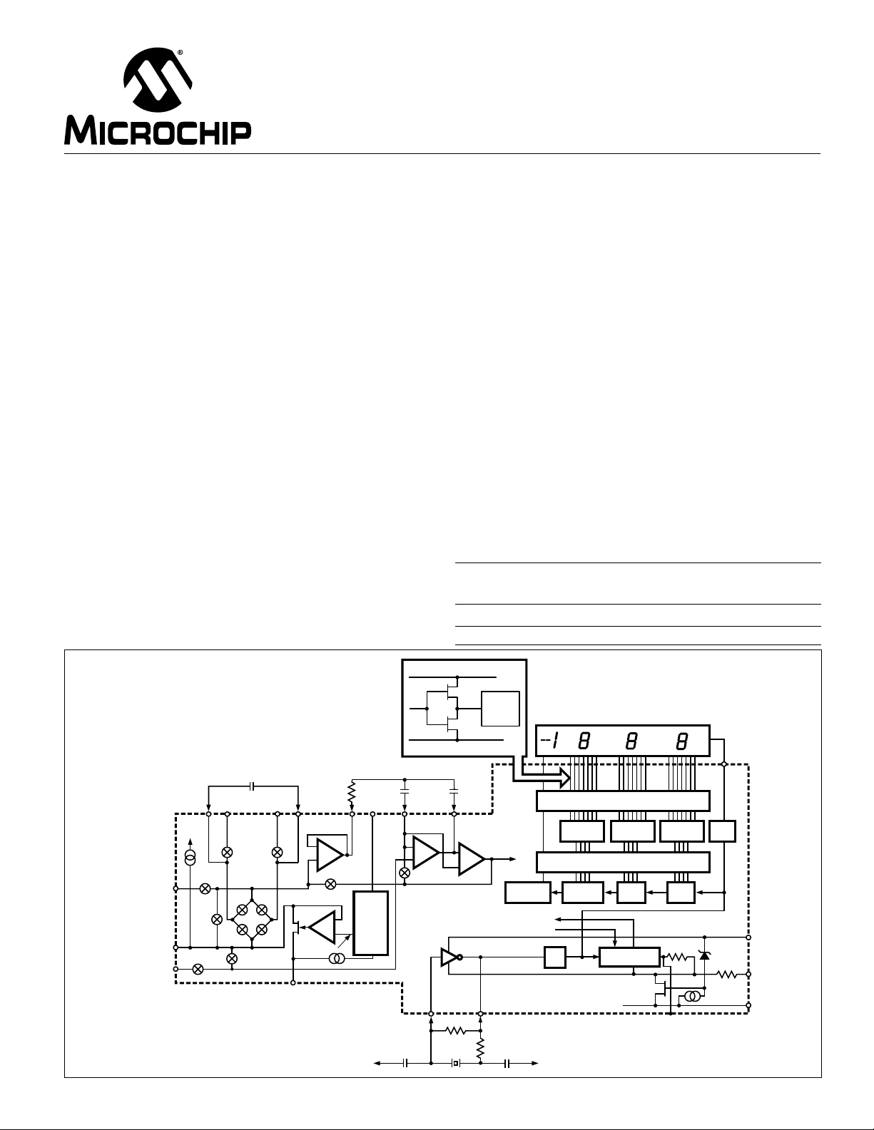
FUNCTIONAL BLOCK DIAGRAM
µV
p-p
10pA Max
TYPICAL APPLICATIONS
■ Thermometry
■ Digital Meters
— Voltage/Current/Power
— pH Measurement
— Capacitance/Inductance
— Fluid Flow Rate/Viscosity
— Humidity
— Position
■ Panel Meters
■ LVDT Indicators
■ Portable Instrumentation
■ Digital Scales
■ Process Monitors
■ Gaussometers
■ Photometers
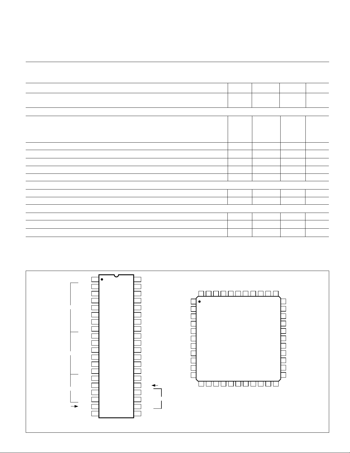
ORDERING INFORMATION
Temp. Max V
Part No. Package Range Temp. Co.
TC811CKW 44-Pin PQFP
TC811CPL
40-Pin Plastic DIP 0°C to +70°C
0°C to +70°C
75 ppm/°C
75 ppm/°C
REF
V
ANALOG
COMMON
V
TYPICAL SEGMENT OUTPUT
0.5mA
2mA
INTERNAL DIGITAL GROUND
TC811CPL
C
C
V
+
REF
DE (+)
REF
ZI & A/Z
DE
(–)DE(+)
AZ & DE (±)
V
DE (–)
–
REF
–
C
REF
33
ZI &
A/Z
V+– 3.0V
26
–
V
+
C
REF
10
µA
31
+
IN
INT
A/Z
32
30
–
IN
INT
R
INT
V
–
+
BUFF
ZI
–
+
28
LOW
TEMPCO
V
REF
V
V
+
AZ
+
29
38
INTEGRATOR
+
A/Z
OSC
10pF
V
27343635
–
COMPARATOR
FROM COMPARATOR OUTPUT
CLOCK
40
1
22MΩ
470k
V
SEGMENT
OUTPUT
C
INT
INT
DIGITAL
SECTION
+
–
TO SWITCH DRIVERS
39
OSC
2
20pF
+
TO
THOUSANDS
f
OSC
INTERNAL DIGITAL GOUND
V
4
+
7 SEGMENT
DECODE
HUNDREDS
LCD DISPLAY
LCD SEGMENT DRIVERS
7 SEGMENT
DECODE
DATA LATCH
TENS UNITS
CONTROL LOGIC
V
TH
= 1V
7 SEGMENT
DECODE
≈70kΩ
1
HLDR
BACKPLANE
21
200
6.2V
Ω
500
38
+
V
TEST
26
–
V
© 2001 Microchip Technology Inc. DS21472A
TC811-7 11/5/96
Page 2

TC811
3-1/2 Digit Analog-To-Digital Converter with
Hold and Differential Reference Inputs
GENERAL DESCRIPTION
The TC811 is a low power, 3-1/2 digit, LCD display
analog-to-digital converter. This device incorporates both a
display hold feature and differential reference inputs. A
crystal oscillator, which only requires two pins, permits
added features while retaining a 40-pin package. An additional feature is an "Integrator Output Zero" phase which
guarantees rapid input overrange recovery.
The TC811 display hold (HLDR) function can be used to
"freeze" the LCD display. The displayed reading will remain
indefinitely as long as HLDR is held high. Conversions
continue but the output data display latches are not updated.
The TC811 also includes a differential reference for easy
ratiometric measurements. Circuits which use the
7106/26/36 can easily be upgraded to include the hold
function with the TC811.
The TC811 has an improved internal zener reference
voltage circuit which maintains the Analog Common temperature drift to 35ppm/°C (typical) and 75ppm/°C (maximum). This represents an improvement of two to four times
over similar 3-1/2 digit converters, eliminating the need for
a costly, space consuming external reference source.
The TC811 limits linearity error to less than one count on
both the 200mV and the 2.00V full-scale ranges. Rollover
error—the difference in readings for equal magnitude but
opposite polarity input signals—is below ±1 count. High
impedance differential inputs offer 1pA leakage currents
and a 10
mance guarantees a “rock solid” reading. The Auto Zero
cycle guarantees a zero display readout for a zero volt input.
devices for a 3-1/2 digit analog to digital converter to directly
drive an LCD display. On-board oscillator, precision voltage
reference and display segment and backplane drivers sim-
12
Ω input impedance. The 15µV
noise perfor-
p-p
The single chip CMOS TC811 incorporates all the active
plify system integration, reduce board space requirements
and lower total cost. A low cost, high resolution (0.05%)
indicating meter requires only a TC811, an LCD display, five
resistors, six capacitors, a crystal, and a 9V battery. Compact, hand held multimeter designs benefit from the Microchip Semiconductor small footprint package option.
The TC811 uses a dual slope conversion technique
which will reject interference signals if the converters integration time is set to a multiple of the interference signal
period. This is especially useful in industrial measurement
environments where 50, 60 and 400Hz line frequency signals are present.
ABSOLUTE MAXIMUM RATINGS*
Supply Voltage (V+ to V–)............................................15V
Analog Input voltage (Either Input)1.....................V+ to V
Reference Input Voltage ...................................... V+ to V
Clock Input ...................................................... TEST to V
Power Dissipation2 (TA ≤ 70°C)
44-Pin Flat Package .........................................1.00W
40-Pin Plastic DIP.............................................1.23W
Operating Temperature Range
Commercial Package (C) ......................0°C to +70°C
Industrial Package (I)........................– 25°C to +85°C
Storage Temperature Range ................– 65°C to +150°C
Lead Temperature (Soldering, 10 sec) .................+300°C
*Static-sensitive device. Unused devices must be stored in conductive
material. Protect devices from static discharge and static fields. Stresses
above those listed under "Absolute Maximum Ratings" may cause permanent damage to the device. These are stress ratings only and functional
operation of the device at these or any other conditions above those
indicated in the operation sections of the specifications is not implied.
Exposure to absolute maximum rating conditions for extended periods may
affect device reliability.
–
–
+
ELECTRICAL CHARACTERISTICS: V
Supply
= 9V, f
= 32.768kHz, and TA = 25°C, unless otherwise noted.
CLOCK
Symbol Parameter Test Conditions Min Typ Max Unit
Input
— Zero Input Reading VIN = 0V – 000.0 ±000.0 +000.0 Digital
VFS = 200mV Reading
— Zero Reading Drift VIN = 0V, 0°C ≤ TA ≤ 70°C — 0.2 1 µV/°C
— Ratiometric Reading VIN = V
NL Linearity Error VFS = 200mV or 2.000V – 1 ±0.2 +1 Counts
E
R
e
N
I
L
CMRR Common-Mode Rejection VCM = ±1V, VIN = 0V, — 50 — µV/V
TC811-7 11/5/96
Roll Over Error VIN– = VIN+ ≈ 200mV – 1 ±0.2 +1 Counts
Noise VIN = 0V, VFS = 200mV — 15 — µV
Input Leakage Current VIN = 0V — 1 10 pA
VFS = 200mV
REF
, V
= 100mV 999 999/1000 1000 Digital
REF
2
© 2001 Microchip Technology Inc. DS21472A
Reading
P-P
Page 3
3-1/2 Digit Analog-To-Digital Converter with
Hold and Differential Reference Inputs
TC811
ELECTRICAL CHARACTERISTICS: V
Supply
= 9V, f
= 32.768kHz, and TA = 25°C, unless otherwise noted.
CLOCK
Symbol Parameter Test Conditions Min Typ Max Unit
TC
SF
Scale Factor Temperature VIN = 199mV, 0°C ≤ TA ≤ 70°C — 1 5 ppm/°C
Coefficient (ext. V
tc = 0ppm)
REF
Analog Common Section
V
CTC
V
C
Analog Common 250KΩ from V+ to Analog Common — — — —
Temperature Coefficient 0°C ≤ T
≤ 70°C————
A
"C" Commercial — 35 75 ppm/°C
"I" Industrial — 35 100 ppm/°C
Analog Common Voltage 250kΩ from V+ to Analog Common 2.7 3.05 3.35 Volts
Hold Pin Input Section
Input Resistance Pin 1 to Pin 37 — 70 — kΩ
V
IL
V
IH
LCD Drive Section
V
SD
V
SD
Input Low Voltage Pin 1 — — Test +1.5 V
Input High Voltage Pin 1 V+ – 1.5 — — V
3
LCD Segment Drive Voltage V+ to V– = 9V 4 5 6 V
LCD Backplane Drive Voltage V+ to V– = 9V 4 5 6 V
P-P
P-P
Power Supply
I
SUP
NOTES: 1. Input voltages may exceed supply voltages when input current is limited to 100µA.
2. Dissipation rating assumes device is mounted with all leads soldered to a printed circuit board.
3. Backplane drive is in phase with the segment drive for "segment off" 180° out of phase for "segment on." Frequency is 20 times the
Power Supply Current VIN = 0V, V+ to V– = 9V — — — —
f
= 16kHz — 70 100 µA
OSC
f
= 48kHz — 90 125 µA
OSC
conversion rate. Average DC component is less than 50mV.
PIN CONFIGURATIONS
HLDR
D
C
B
1's
A
F
G
E
D
C
B
10's
A
F
E
D
B
100's
1000's
(MINUS SIGN)
F
E
AB
POL
1
NORMAL PIN
2
CONFIGURATION
1
3
1
4
1
5
1
6
1
7
1
8
1
2
2
2
2
2
2
3
3
3
3
4
NC = NO INTERNAL CONNECTION
9
10
11
12
13
14
15
16
17
18
19
20
TC811CPL
(40-PIN PDIP)
40
39
38
37
36
35
34
33
32
31
30
29
28
27
26
25
24
23
22
21
OSC
1
OSC
2
+
V
TEST
+
V
REF
+
C
REF
–
C
REF
–
V
REF
ANALOG
COMMON
+
V
IN
–
V
IN
C
AZ
V
BUFF
V
INT
–
V
G
10's
2
C
3
100's
A
3
G
3
BP
(BACKPLANE)
TEST
V
OSC
OSC
HLDR
+
+
REF
REF
C
V
44 43 42 41 39 3840
1
NC
2
NC
3
+
4
NC
5
6
2
7
1
8
D
9
1
10
C
1
11
B
1
12 13 14 15 17 18
1F1G1E1
A
–
REF
C
–
REF
COM
V
TC811CKW
16
D2C2B2A
+
IN
V
(PQFP)
–
IN
V
C
37AZ36
19 20 21 22
2F2E2
BUFF35INT
–
VVV
34
33
NC
32
G
2
C
31
3
30
A
3
29
G
3
BP
28
POL
27
26
AB
4
E
25
3
F
24
3
23
B
3
3
D
© 2001 Microchip Technology Inc. DS21472A
3
TC811-7 11/5/96
Page 4

TC811
PIN DESCRIPTION
Pin No.
40-Pin Plastic DIP Symbol Description
1 HLDR Hold pin, logic 1 holds present display reading.
2D1Activates the D section of the units display.
3C1Activates the C section of the units display.
4B1Activates the B section of the units display.
5A1Activates the A section of the units display.
6F1Activates the F section of the units display.
7G1Activates the G section of the units display.
8E1Activates the E section of the units display.
9D2Activates the D section of the tens display.
10 C
11 B
12 A
13 F
14 E
15 D
16 B
17 F
18 E
19 AB
2
2
2
2
2
3
3
3
3
4
20 POL Activates the negative polarity display.
21 BP Backplane drive output.
22 G
23 A
24 C
25 G
26 V
27 V
28 V
29 C
30 V
31 V
3
3
3
2
–
INT
BUFF
AZ
–
IN
+
IN
32 COM Analog Common: Internal zero reference.
33 V
34 C
35 C
36 V
–
REF
–
REF
+
REF
+
REF
37 TEST All LCD segment test when pulled high (V+).
38 V
39 OSC
40 OSC
+
2
1
Activates the C section of the tens display.
Activates the B section of the tens display.
Activates the A section of the tens display.
Activates the F section of the tens display.
Activates the E section of the tens display.
Activates the D section of the hundreds display.
Activates the B section of the hundreds display.
Activates the F section of the hundreds display.
Activates the E section of the hundreds display.
Activates both halves of the 1 in the thousands display.
Activates the G section of the hundreds display.
Activates the A section of the hundreds display.
Activates the C section of the hundreds display.
Activates the G section of the tens display.
Negative power supply voltage.
Integrator output, connection for C
Buffer output, connection for R
Integrator input, connection for CAZ.
Analog input low.
Analog input high.
Reference input low.
Negative connection for reference capacitor.
Positive connection for reference capacitor.
Reference input high.
Positive power supply voltage.
Crystal oscillator output.
Crystal oscillator input.
3-1/2 Digit Analog-To-Digital Converter with
Hold and Differential Reference Inputs
.
INT
.
INT
TC811-7 11/5/96
4
© 2001 Microchip Technology Inc. DS21472A
Page 5
3-1/2 Digit Analog-To-Digital Converter with
Hold and Differential Reference Inputs
TC811
0.1µF
33
+
ANALOG
INPUT
–
1MΩ
0.01µF
180kΩ
0.068µF
35
34
+
C
C
REF
REF
31
+
V
IN
–
30
V
TC811
IN
ANALOG
32
COMMON
28
V
BUFF
0.47
µF
29
C
AZ
27
V
INT
OSC
2
39 40
22MΩ
470k
20pF
+
V
9–19
22–25
POL
HLDR
V
V
OSC
BP
V
+
REF
–
REF
V
+
–
1
SEGMENT
DRIVE
20
MINUS SIGN
21
38
1
36
33
26
10pF
TO ANALOG COMMON
(PIN 32)
LCD
BACKPLANE
240kΩ
+
10k
Ω
2 CONVERSION/SEC
+
V
9V
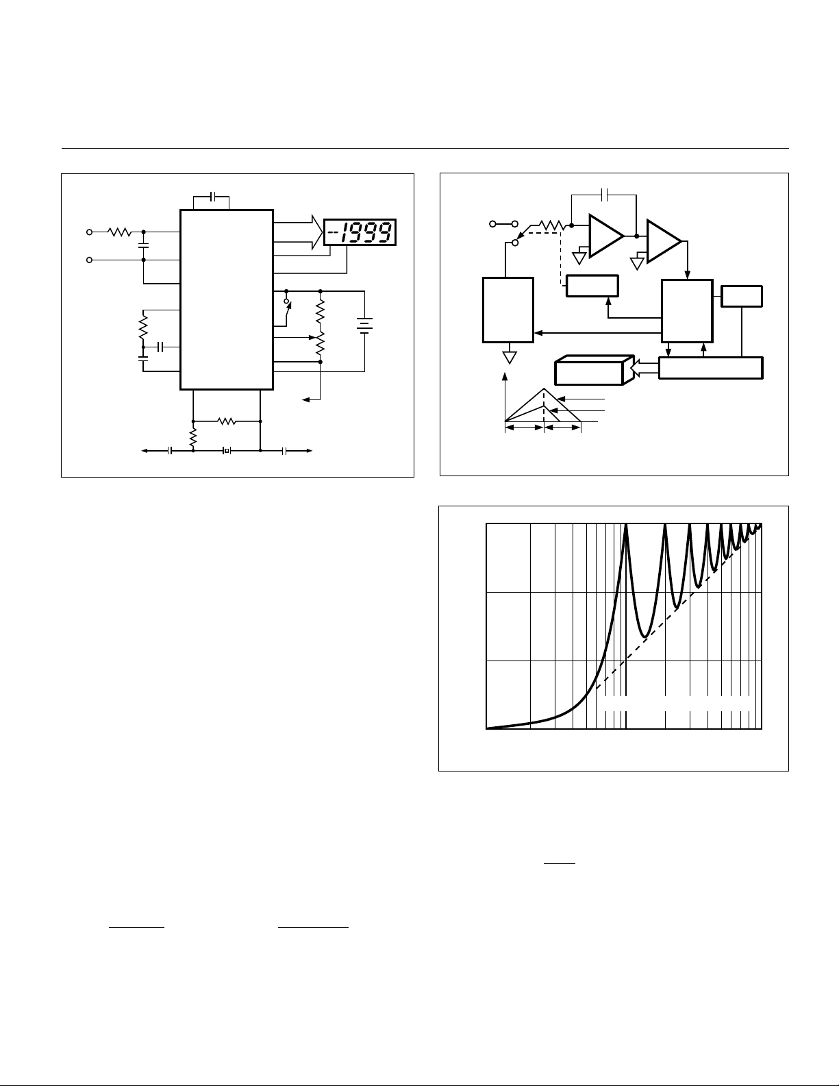
Figure 1. Typical Operating Circuit
GENERAL THEORY OF OPERATION
Dual-Slope Conversion Principles
(All Pin Designations Refer to 40-Pin DIP Package)
The TC811 is a dual slope, integrating analog-to-digital
converter. An understanding of the dual slope conversion
technique will aid the user in following the detailed TC811
theory of operation following this section. A conventional
dual slope converter measurement cycle has two distinct
phases:
1) Input Signal Integration
2) Reference Voltage Integration (Deintegration)
Referring to Figure 2, the unknown input signal to be
converted is integrated from zero for a fixed time period
(T
), measured by counting clock pulses. A constant
INT
reference voltage of the opposite polarity is then integrated
until the integrator output voltage returns to zero. The
reference integration (deintegration) time (T
directly proportional to the unknown input voltage (VIN).
In a simple dual slope converter, a complete conversion
requires the integrator output to “ramp-up” from zero and
“ramp-down” back to zero. A simple mathematical equation
relates the input signal, reference voltage and integration
time:
t
1 V
R
INT CINT
INT
VIN(t) dt =
∫
R
0
REF tDEINT
INT CINT
DEINT
) is then
ANALOG
INPUT
SIGNAL
+/–
REF
VOLTAGE
OUTPUT
INTEGRATOR
FIXED
SIGNAL
INTEGRATE
TIME
INTEGRATOR
SWITCH
DRIVER
POLARITY CONTROL
DISPLAY
VARIABLE
REFERENCE
INTEGRATE
TIME
Figure 2. Basic Dual Slope Converter
30
20
10
NORMAL MODE REJECTION (dB)
0
0.1/T 1/T 10/T
INPUT FREQUENCY
Figure 3. Normal-Mode Rejection of
Dual Slope Converter
For a constant V
VIN = V
REF
[
INT
t
:
DEINT
t
INT
C
PHASE
CONTROL
V
≈
IN
FULL SCALE
1.2 V
≈
IN
COMPARATOR
–
+
CONTROL
LOGIC
COUNTER
FULL SCALE
–
+
V
V
T = MEASUREMENT PERIOD
]
CLOCK
where:
V
= Reference voltage
REF
t
= Integration Time
INT
t
= Deintegration Time
DEINT
© 2001 Microchip Technology Inc. DS21472A
5
TC811-7 11/5/96
Page 6

3-1/2 Digit Analog-To-Digital Converter with
TC811
Accuracy in a dual slope converter is unrelated to the
integrating resistor and capacitor values as long as they are
stable during a measurement cycle. An inherent benefit of
the dual slope technique is noise immunity. Noise spikes are
integrated or averaged to zero during the integration periods, making integration ADCs immune to the large conversion errors that plague successive approximation converters in high noise environments. Interfering signals, with
frequency components at multiples of the averaging (integrating) period, will be attenuated. (see Figure 3). Integrating ADCs commonly operate with the signal integration
period set to a multiple of the 50/60Hz power line period.
Hold and Differential Reference Inputs
INT
DE-INT
ZI
AZ
1000
1–2000
11–140
910–2900
4000
THEORY OF OPERATION
Analog Section
In addition to the basic integrate and deintegrate dualslope cycles discussed above, the TC811 design incorporates an “Integrator Output Zero” cycle and an “Auto Zero”
cycle. These additional cycles ensure the integrator starts at
0V (even after a severe overrange conversion) and that all
offset voltage errors (buffer amplifier, integrator and comparator) are removed from the conversion. A true digital zero
reading is assured without any external adjustments.
A complete conversion consists of four distinct phases:
(1) Integrator Output Zero Cycle
(2) Auto Zero Cycle
(3) Signal Integrate Cycle
(4) Reference Deintegrate Cycle
Integrator Output Zero Cycle
This phase guarantees that the integrator output is at
zero volts before the system zero phase is entered, ensuring
that the true system offset voltages will be compensated for
even after an overrange conversion. The duration of this
phase is variable, being a function of the number of counts
(clock cycles) required for deintegration.
The Integrator Output Zero cycle will last from 11 to 140
counts for non-over-range conversions and from 31 to 640
counts for overrange conversions.
Auto Zero Cycle
During the Auto Zero cycle, the differential input signal
is disconnected from the measurement circuit by opening
internal analog switches and the internal nodes are shorted
to Analog Common (0V ref.) to establish a zero input
condition. Additional analog switches close a feedback loop
around the integrator and comparator to permit comparator
offset voltage error compensation. A voltage established on
CAZ then compensates for internal device offset voltages
during the measurement cycle. The Auto Zero cycle residual
TC811-7 11/5/96
Figure 4a. Conversion Timing During Normal Operation
INT
DE-INT
ZI
AZ
Figure 4b. Conversion Timing During Overrange Operation
1000
2001–2090
31–640
300–910
4000
is typically 10 to 15µV.
The Auto Zero duration is from 910 to 2,900 counts for
non-over-range conversions and from 300 to 910 counts for
overrange conversions.
Signal Integration Cycle
Upon completion of the Auto Zero cycle, the Auto Zero
loop is opened and the internal differential inputs connect to
+
V
and V
IN
for a fixed time period which, in the TC811 is 1000 counts
(4000 clock periods). The externally set clock frequency is
divided by four before clocking the internal counters. The
integration time period is:
T
The differential input voltage must be within the device
common-mode range when the converter and measured
system share the same power supply common (ground).
If the converter and measured system do not share the same
power supply common, as in battery powered applications,
–
V
should be tied to Analog Common.
IN
6
INT
–
. The differential input signal is then integrated
IN
4000
=
f
OSC
© 2001 Microchip Technology Inc. DS21472A
Page 7

3-1/2 Digit Analog-To-Digital Converter with
Hold and Differential Reference Inputs
TC811
Polarity is determined at the end of signal integration
phase. The sign bit is a “true polarity” indication in that
signals less than 1 LSB are correctly determined. This
allows precision null detection which is limited only by device
noise and Auto Zero residual offsets.
Reference Integrate (Deintegrate) Cycle
The reference capacitor, which was charged during the
Auto Zero cycle, is connected to the input of the integrating
amplifier. The internal sign logic insures that the polarity of
the reference voltage is always connected in the phase
which is opposite to that of the input voltage. This causes the
integrator to ramp back to zero at a constant rate which is
determined by the reference potential.
The amount of time required (T
amplifier to reach zero is directly proportional to the amplitude of the voltage that was put on the integrating capacitor
(V
) during the integration cycle:
INT
R
T
DEINT
INT CINT VINT
=
V
REF
The digital reading displayed Is:
+
V
– V
Digital Count = 1000
IN
V
REF
The oscillator frequency is divided by 4 prior to clocking
the internal decade counters. The four phase measurement
cycle takes a total of 4000 counts or 16000 clock pulses. The
4000 count cycle is independent of input signal magnitude
or polarity.
Each phase of the measurement cycle has the following
length:
) for the integrating
DEINT
–
IN
power dissipation, and improve the overall performance.
(see Oscillator Components)
Digital Section
The TC811 contains all the segment drivers necessary
to directly drive a 3-1/2 digit liquid crystal display (LCD). An
LCD backplane driver is included. The backplane frequency
is the external clock frequency divided by 800. For three
conversions/second the backplane frequency is 60Hz with
a 5V nominal amplitude. When a segment driver is in phase
with the backplane signal the segment of “OFF”. An out of
phase segment drive signal causes the segment to be “ON”
or visible. This AC drive configuration results in negligible
DC voltage across each LCD segment. This insures long
LCD display life. The polarity segment driver is “ON” for
negative analog inputs. If V
+
and V
IN
–
are reversed then this
IN
indicator would reverse.
TEST Function (TEST)
On the TC811, when TEST is pulled to a logical “HIGH”,
all segments are turned “ON”. The display will read “-1888”.
During this mode the LCD segments have a constant DC
voltage impressed. Do not leave the display in this mode for
more than several minutes. LCD displays may be destroyed
if operated with DC levels for extended periods.
The display FONT and segment drive assignment are
shown in Figure 5.
DISPLAY FONT
1) Auto Zero: 300 to 2900 Counts
2) Signal Integrate: 1000 Counts
This time period is fixed. The integration period is:
4000
T
= = 1000 Counts
INT
f
OSC
Where f
is the crystal oscillator frequency.
OSC
3) Reference Integrate: 0 to 2000 Counts
4) Integrator Output Zero: 11 to 640 Counts
The TC811 can replace the ICL7106/26/36 in circuits
which require both the hold function and a differential
reference. The TC811 offers a greatly improved internal
reference temperature coefficient, which can often eliminate
the need for an external reference. Some minor component
changes are required to upgrade existing designs, reduce
© 2001 Microchip Technology Inc. DS21472A
1000's 100's 10's 1's
Figure 5. Display FONT and Segment Assignment
HOLD Reading Input (HLDR)
When HLDR is at a logic “HI” the latch will not be
updated. Conversions will continue but will not be updated
until HLDR is returned to “LOW”. To continuously update the
display, connect HLDR to ground or leave it open. This input
is CMOS compatible and has an internal resistance of 70kΩ
(typical) tied to TEST.
7
TC811-7 11/5/96
Page 8

TC811
3-1/2 Digit Analog-To-Digital Converter with
Hold and Differential Reference Inputs
COMPONENT VALUE SELECTION
Auto Zero Capacitor - C
The value of the Auto Zero capacitor (CAZ) has some
influence on system noise. A 0.47µF capacitor is recommended for 200mV full-scale applications where 1LSB is
100µV. A 0.10µF capacitor should be used for 2.0V fullscale applications. A capacitor with low dielectric absorption
(Mylar) is required.
Reference Voltage Capacitor -C
The reference voltage used to ramp the integrator
output voltage back to zero during the reference integrate
cycle is stored on C
. A 0.1µF capacitor is typical. If the
REF
application requires a sensitivity of 200mV full-scale, increase C
to 1.0µF. Rollover error will be held to less than
REF
1/2 count. A good quality, low leakage capacitor, such as
Mylar, should be used.
Integrating Capacitor - C
CINT should be selected to maximize integrator output
voltage swing without causing output saturation. Analog
common will normally supply the differential voltage reference. For this case a ±2V integrator output swing is optimum
when the analog input is near full-scale. For 2 or 2.5 reading/
second (f
value is suggested. If a different oscillator frequency is used,
C
must be changed in inverse proportion to maintain the
INT
nominal ±2V integrator swing. An exact expression for C
is :
C
INT
= 32kHz or 40kHz) and VFS = 200mV, a .068µF
OSC
=
V
INT RINT fOSC
4000 V
FS
AZ
REF
INT
INT
Oscillator Components
The internal oscillator has been designed to operate
with a quartz crystal, such as the Statek CX-1V series. Such
crystals are very small and are available in a variety of
standard frequencies. Note that f
generate the TC811 internal control clock. The backplane
drive signal is derived by dividing f
To achieve maximum rejection of ac-line noise pickup,
a 40kHz crystal should be used. This frequency will yield an
integration period of 100msec and will reject both 50Hz and
60Hz noise. For prototyping or cost-sensitive applications a
32.768kHz watch crystal can be used, and will produce
about 25dB of line-noise rejection. Other crystal frequencies, from 16kHz to 48kHz, can also be used.
Pins 39 and 40 make up the oscillator section of the
TC811. Figures 6a and 6b show some typical conversion
rate component values.
The LCD backplane frequency is derived by dividing the
oscillator frequency by 800. Capacitive loading of the LCD
may compromise display performance if the oscillator is run
much over 48kHz.
Reference Voltage (V
REF
A full-scale reading (2000 counts) requires the input
signal be twice the reference voltage.
In some applications a scale factor other than unity may
exist, such as between a transducer output voltage and the
required digital reading. Assume, for example, a pressure
transducer output is 400mV for 2000lb/in2. Rather than
dividing the input voltage by two, the reference voltage
should be set to 200mV. This permits the transducer input to
be used directly.
is divided by four to
OSC
by 800.
OSC
)
where:
f
= Clock frequency at Pin 39
OSC
VFS = Full-scale input voltage
R
= Integrating resistor
INT
V
= Desired full-scale integrator output swing
INT
C
must have low dielectric absorption to minimize
INT
roll-over error. A polypropylene capacitor is recommended.
Integrating Resistor -R
INT
The input buffer amplifier and integrator are designed
with class A output stages which have idling currents of 6µA.
The integrator and buffer can supply 1µA drive currents with
negligible linearity errors. R
is chosen to remain in the
INT
output stage linear drive region but not so large that printed
circuit board leakage currents induce errors. For a 200mV
full-scale, R
should be about 180kΩ. A 2.0V full-scale
INT
requires abut 1.8MΩ.
TC811-7 11/5/96
TC811
OSC1
40
22MΩ
40.0 kHz
10pF
Figure 6a. TC811 Oscillator
8
OSC2
470k
20pF
© 2001 Microchip Technology Inc. DS21472A
+
V
3839
9V
+
Page 9

3-1/2 Digit Analog-To-Digital Converter with
R
I
+
–
V
IN
V
C
I
INTEGRATOR
V
I
=
[
[
V
CMVIN
–
INPUT
BUFFER
C
I
=
=
R
I
INTEGRATION CAPACITOR
INTEGRATION RESISTOR
4000
f
INTEGRATION TIMET
I
==
Where:
V
I
CM
OSC
–
+
–
+
T
I
RI C
I
Hold and Differential Reference Inputs
TC811
Oscillator Full-Scale Voltage (VFS)
Freq. (kHz) 200mV 2.0V
RINT CINT RINT CINT
32.768 180k 0.068µF 1.8M 0.068µF
40 150k 0.068µF 1.5M 0.068µF
Figure 6b.
DEVICE PIN FUNCTIONAL DESCRIPTION
Differential Signal Inputs (V
–
V
(Pin 30))
IN
The TC811 is designed with true differential inputs and
accepts input signals within the input stage common mode
voltage range (VCM). The typical range is V+ – 1.0 to V– +
1.5V. Common-mode voltages are removed from the system when the TC811 operates from a battery or floating
power source (isolated from measured system) and V
connected to Analog Common. (see Figure 8)
In systems where common-mode voltages exist, the
86dB common-mode rejection ratio minimizes error. Common-mode voltages do, however, affect the integrator output level. A worse case condition exists if a large positive
VCM exists in conjunction with a full-scale negative differential signal. The negative signal drives the integrator output
positive along with VCM (Figure 8). For such applications the
integrator output swing can be reduced below the recommended 2.0V full-scale swing. The integrator output will
swing within 0.3V of V+ or V– without increased linearity
error.
Reference (V
+
(Pin 36), V
REF
Unlike the ICL7116, the TC811 has a differential reference as well as the “hold” function. The differential reference
inputs permit ratiometric measurements and simplify inter-
+
(Pin 31),
IN
–
(Pin 33))
REF
–
is
IN
facing with sensors such as load cells and temperature
sensors. The TC811 is ideally suited to applications in handheld multimeters, panel meters, and portable instrumentation. The reference voltage can be generated anywhere
within the V+ to V– power supply range.
To prevent rollover type errors from being induced by
large common-mode voltages, C
should be large com-
REF
pared to stray node capacitance. A 0.1µF capacitor is a
typical value.
The TC811 offers a significantly improved Analog Common temperature coefficient. This provides a very stable
voltage suitable for use as a voltage reference. The temperature coefficient of Analog Common is typically
35ppm/°C.
Figure 8. Common-Mode Voltage Reduces Available
Integrator Swing. (V
COM
≠ VIN)
SEGMENT
DRIVE
MEASURED
SYSTEM
© 2001 Microchip Technology Inc. DS21472A
+
–
V
V
POWER
SOURCE
+
V
–
V
GND
GND
Figure 7. Common-Mode Voltage Removed in Battery Operation With V
V
BUF
+
V
–
V
ANALOG
COMMON
V
C
–
REF
AZVINT
TC811
+
V
REF
9
+
V
+
9V
OSC
OSC
–
V
BPPOL
1
2
LCD DISPLAY
20MΩ
470k
–
= Analog Common
IN
10pF
40kHZ
20 pF
+
V
+
V
TC811-7 11/5/96
Page 10

TC811
TC811
BP
TEST
V
+
V
+
GND
TO LCD
DECIMAL
POINT
TO LCD
BACKPLANE
4049
TC811
DECIMAL
POINT
SELECT
V
+
V
+
TEST
GND
4030
TO LCD
DECIMAL
POINTS
BP
HDLR
TO "HOLD"
ANNUNCIATOR
3-1/2 Digit Analog-To-Digital Converter with
Hold and Differential Reference Inputs
Analog Common (Pin 32)
The Analog Common pin is set at a voltage potential
approximately 3.0V below V+. This potential is guaranteed
to be between 2.70V and 3.35V below V+. Analog common
is tied internally to an N channel FET capable of sinking
100µA. This FET will hold the common line at 3.0V below V
should an external load attempt to pull the common line
toward V+. Analog common source current is limited to 1µA.
Analog common is therefore easily pulled to a more negative
voltage (i.e. below V+ – 3.0V).
The TC811 connects the internal V
Analog Common during the Auto Zero cycle. During the
reference integrate phase V
mon. If V
–
is not externally connected to Analog Common,
IN
–
is connected to Analog Com-
IN
a common-mode voltage exists. This is rejected by the
converter’s 86dB common-mode rejection ratio. In battery
powered applications, Analog Common and V
connected, removing common-mode voltage concerns. In
systems where V
or to a given voltage, Analog Common should be connected
–
to V
.
IN
–
is connected to the power supply ground
IN
The Analog Common pin serves to set the analog
section reference or common point. The TC811 is specifically designed to operate from a battery or in any measurement system where input signals are not referenced (float)
with respect to the TC811 power source. The Analog Common potential of V+ – 3.0V gives a 7V end of battery life
voltage. The analog common potential has a voltage coefficient of 0.001%/%.
With a sufficiently high total supply voltage (V+ – V– >
7.0V), Analog Common is a very stable potential with
excellent temperature stability (typically 35ppm/°C). This
potential can be used to generate the TC811 reference
voltage. An external voltage reference will be unnecessary
in most cases because of the 35ppm/°C temperature coefficient. See TC811 Internal Voltage Reference discussion.
TEST (Pin 37)
The TEST pin potential is 5V less the V+. TEST may be
used as the negative power supply connection when interfacing the TC811 to external CMOS logic. The TEST pin is
tied to the internally generated negative logic supply through
a 500Ω resistor. The TEST pin may be used to sink up to
1mA. See the applications section for additional information
on using TEST as a negative digital logic supply.
If TEST is pulled “HIGH” (V+), all segments plus the
minus sign will be activated. Do not operate in this mode for
more than several minutes, because when TEST is pulled to
V+, the LCD Segments are impressed with a DC voltage
which may cause damage to the LCD.
TC811-7 11/5/96
+
and V
IN
–
IN
–
inputs to
IN
are usually
APPLICATIONS INFORMATION
Decimal Point and Annunciator Drive
The TEST pin is connected to the internally generated
digital logic supply ground through a 500Ω resistor. The
TEST pin may be used as the negative supply for external
+
CMOS gate segment drivers. LCD display annunciators for
decimal points, low battery indication, or function indication
may be added without adding an additional supply. No more
than 1mA should be supplied by the TEST pin. The TEST pin
potential is approximately 5V below V+.
Internal Voltage Reference
The TC811 Analog Common voltage temperature stability has been significantly improved. This improved device
can be used to upgrade old systems and design new
systems without external voltage references. External R and
C values do not need to be changed, however, noise
performance will be improved by increasing CAZ (See Auto
Zero Capacitor section). Figure 10 shows Analog Common
supplying the necessary voltage reference for the TC811.
Figure 9. Display Annunciator Drivers
10
© 2001 Microchip Technology Inc. DS21472A
Page 11

3-1/2 Digit Analog-To-Digital Converter with
Hold and Differential Reference Inputs
TC811
Liquid Crystal Display Sources
Several LCD manufactures supply standard LCD displays to interface with the TC811 3-1/2 digit analog-to-digital
converter.
Representative
Manufacturer Address/Phone Part Numbers
Crystaloid 5282 Hudson Dr., C5335, H5535,
Electronics Hudson, OH 44236 T5135, SX440
216-655-2429
AND 770 Airport Blvd., FE 0801,
Burlingame, CA 94010 FE 0203
415-347-9916
EPSON 3415 Kashikawa St., LD-B709BZ
Torrence, CA 90505 LD-H7992AZ
212-534-0360
Hamlin, Inc. 612 E. Lake St., 3902, 3933, 3903
Lake Mills, WI 53551
414-648-2361
*
NOTE:
Contact LCD manufacturer for full product listing/specifications.
*
Oscillator Crystal Source
Representative
Manufacturer Address/Phone Part Numbers
STATEK 512 N-Main CX-1V 40.0
Orange, CA 92668
714-639-7810
Ratiometric Resistance Measurements
The TC811 true differential input and differential reference make ratiometric readings possible. In ratiometric
operation, an unknown resistance is measured with respect
to a known standard resistance. No accurately defined
reference voltage is needed.
The unknown resistance is put in series with a known
standard and a current is passed through the pair (Figure
11). The voltage developed across the unknown is applied
to the input and the voltage across the known resistor
applied to the reference input. If the unknown equals the
standard, the input voltage will equal the reference voltage
and the display will read 1000. The displayed reading can be
determined from the following expression:
9V
+
V
+
V
REF
–
V
REF
= 1/2 V
REF
+
V
REF
–
V
REF
+
V
IN
–
V
IN
ANALOG
COMMON
38
+
36
V
REF
33
32
FULL SCALE
+
V
TC811
240kΩ
10kΩ
HLDR
LCD
26
–
V
TC811
ANALOG
COMMON
SET V
Figure 10. TC811 Internal Voltage Reference Connection
R
STANDARD
R
UNKNOWN
Figure 11. Low Parts Count Ratio Metric Resistance Measurement
R
Displayed reading = x 1000
UNKNOWN
R
STANDARD
The display will overrange for R
R
STANDARD
© 2001 Microchip Technology Inc. DS21472A
.
UNKNOWN
≥ 2 X
11
TC811-7 11/5/96
Page 12

TC811
3-1/2 Digit Analog-To-Digital Converter with
Hold and Differential Reference Inputs
9V
+
9V
+
160 kΩ 300 kΩ 300 kΩ
1N4148
SENSOR
50 kΩ
R
2
50 kΩ
R
1
Figure 12. Temperature Sensor
PACKAGE DIMENSIONS
+
V
–
V
IN
TC811
+
V
IN
VFS = 200 MV
+
V
REF
–
V
REF
COMMON
–
V
HLDR V
40-Pin Plastic DIP
+
PIN 1
0.7%/°C
PTC
5.6 kΩ 160 kΩ
1N914
R
3
R
20 kΩ
R
20 kΩ
1
2
+
V
–
V
TC811
IN
+
V
IN
+
V
REF
–
V
REF
COMMON
–
V
HLDR V
Figure 13. Positive Temperature Coefficient
Resistor Temperature Sensor
+
.200 (5.08)
.140 (3.56)
.150 (3.81)
.115 (2.92)
TC811-7 11/5/96
.110 (2.79)
.090 (2.29)
2.065 (52.45)
2.027 (51.49)
.070 (1.78)
.045 (1.14)
.022 (0.56)
.015 (0.38)
.555 (14.10)
.530 (13.46)
.040 (1.02)
.020 (0.51)
12
.015 (0.38)
.008 (0.20)
.610 (15.49)
.590 (14.99)
3° MIN.
.700 (17.78)
.610 (15.50)
Dimensions: inches (mm)
© 2001 Microchip Technology Inc. DS21472A
Page 13

3-1/2 Digit Analog-To-Digital Converter with
Hold and Differential Reference Inputs
PACKAGE DIMENSIONS (CONT.)
44-Pin QFP
TC811
7° MAX.
PIN 1
.018 (0.45)
.012 (0.30)
.031 (0.80) TYP.
.398 (10.10)
.390 (9.90)
.557 (14.15)
.537 (13.65)
.398 (10.10)
.390 (9.90)
.557 (14.15)
.537 (13.65)
.009 (0.23)
.005 (0.13)
.096 (2.45) MAX.
.041 (1.03)
.026 (0.65)
.010 (0.25) TYP.
.083 (2.10)
.075 (1.90)
Dimensions: inches (mm)
© 2001 Microchip Technology Inc. DS21472A
13
TC811-7 11/5/96
Page 14

TC811
3-1/2 Digit Analog-To-Digital Converter with
Hold and Differential Reference Inputs
W
ORLDWIDE SALES AND SERVICE
AMERICAS
Corporate Office
2355 West Chandler Blvd.
Chandler, AZ 85224-6199
Tel: 480-792-7200 Fax: 480-792-7277
Technical Support: 480-792-7627
Web Address: http://www.microchip.com
Rocky Mountain
2355 West Chandler Blvd.
Chandler, AZ 85224-6199
Tel: 480-792-7966 Fax: 480-792-7456
Atlanta
500 Sugar Mill Road, Suite 200B
Atlanta, GA 30350
Tel: 770-640-0034 Fax: 770-640-03 07
Austin
Analog Product Sales
8303 MoPac Expressway North
Suite A-201
Austin, TX 78759
Tel: 512-345-2030 Fax: 512-345-60 85
Boston
2 Lan Drive, Suite 120
Westford, MA 01886
Tel: 978-692-3848 Fax: 978-692-38 21
Boston
Analog Product Sales
Unit A-8-1 Millbrook T arry Condominium
97 Lowell Road
Concord, MA 01742
Tel: 978-371-6400 Fax: 978-371-00 50
Chicago
333 Pierce Road, Suite 180
Itasca, IL 60143
Tel: 630-285-0071 Fax: 630-285 -00 75
Dallas
4570 Westgrove Drive, Suite 160
Addison, TX 75001
Tel: 972-818-7423 Fax: 972-818-29 24
Dayton
Two Prestige Place, Suite 130
Miamisburg, OH 45342
Tel: 937-291-1654 Fax: 937-291-91 75
Detroit
Tri-Atria Office Building
32255 Northwestern Highway, Suite 190
Farmington Hills, MI 48334
Tel: 248-538-2250 Fax: 248-538 -22 60
Los Angele s
18201 Von Karman, Suite 1090
Irvine, CA 92612
Tel: 949-263-1888 Fax: 949-263-13 38
Mountain View
Analog Product Sales
1300 Terra Bella Avenue
Mountain View, CA 94043-1836
Tel: 650-968-9241 Fax: 650-967-15 90
All rights reserved. © 2001 Microchip Technology Incorporated. Printed in the USA. 1/01 Printed on recycled paper.
Information contained in this publication regarding device applications and the like is intended through suggestion only and may be superseded by
updates. It is your re sponsib ility to en sure that your applicatio n meets w ith your specifications . No re presen tation or warrant y is given and no liability is
assumed by Micro chip Technology Incorporated with re spec t to the accur acy or use of such infor mation, or infringem ent of paten ts or other intell ectual
property rights arising from such use or otherwise. Use of Microchipís products as critical components in life support systems is not authori zed ex ce pt wi th
express written approval by Microchip. No licenses are conveyed, implicitly or otherwise, except as maybe explicitly expressed herein, under any intellectual property rights. The Mi crochip logo and name are registered trad emarks of Microchip Technology Inc. in the U.S.A. and other countries. All rights
reserved. All other trademarks mentioned herein are the property of their respective companies.
New York
150 Motor Parkway, Suite 202
Hauppauge, NY 11788
Tel: 631-273-5305 Fax: 631-273-5335
San Jose
Microchip Technology Inc.
2107 North First Street, Suite 590
San Jose, CA 95131
Tel: 408-436-7950 Fax: 408-436-7955
Toronto
6285 Northam Drive, Suite 108
Mississa uga, Ontario L4V 1X5, C anada
Tel: 905-673-0699 Fax: 905-673-6509
ASIA/PACIFIC
China - Beijing
Microchip Technology Beijing Office
Unit 915
New China Hong Kong Manhattan Bldg.
No. 6 Chaoyangmen Beidajie
Beijing, 100027, No. China
Tel: 86-10-85282100 Fax: 86-10-85282104
China - Shanghai
Microchip Technology Shanghai Office
Room 701, Bldg. B
Far East Int ernational Plaza
No. 317 Xian Xia Road
Shanghai, 200051
Tel: 86-21-6275-5700 Fax: 86-21-6275-5060
Hong Kong
Microchip Asia Pacific
RM 2101, Tower 2, Metroplaza
223 Hing Fong Road
Kwai Fong, N.T., Hong Kong
Tel: 852-2401-1200 Fax: 852-2401-3431
India
Microchip Technology Inc.
India Liaison Office
Divyasree Chambers
1 Floor, Wing A (A3/A4)
No. 11, OíShaugnessey Road
Bangalore, 560 025, India
Tel: 91-80-2290061 Fax: 91-80-2290062
Japan
Microchip Technology Intl. Inc.
Benex S-1 6F
3-18-20, Shinyokohama
Kohoku-Ku, Yokohama-shi
Kanagawa, 222-0033, Japan
Tel: 81-45-471- 6166 Fax: 81-45-471-6122
Korea
Microchip Technology Korea
168-1, Youngbo Bldg. 3 Floor
Samsung-Dong, Kangnam-Ku
Seoul, Korea
Tel: 82-2-554-7200 Fax: 82-2-558-5934
ASIA/PACIFIC
(continued)
Singapore
Microchip Technology Singapore Pte Ltd.
200 Middle Road
#07-02 Prime Centre
Singapore, 188980
Tel: 65-334-8870 Fax: 65-334-8850
Taiwan
Microchip Technology Taiwan
11F-3 , No . 20 7
Tung Hua North Road
Taipei, 105, Taiwan
Tel: 886-2-2717-7175 Fax: 886-2-2545-0139
EUROPE
Australia
Microchip Technology Australia Pty Ltd
Suite 22, 41 Rawson Street
Epping 2121, NSW
Australia
Tel: 61-2-9868-6733 Fax: 61-2-9868-67 55
Denmark
Microchip Technology Denmark ApS
Regus Business Centre
Lautrup hoj 1-3
Ballerup D K-2750 Denmark
Tel: 45 4420 9895 Fax: 45 4420 9910
France
Arizona Microchip Technology SARL
Parc díActivite du Moulin de Massy
43 Rue du Saule Trapu
Batiment A - ler Etage
91300 Massy, France
Tel: 33-1-69-53-63-20 Fax: 33-1-69-30-90-79
Germany
Arizona Microchip Technology GmbH
Gustav-Heinemann Ring 125
D-81739 Munich, Germany
Tel: 49-89-627-144 0 Fax: 49-89-627-144-44
Germany
Analog Product Sales
Lochhamer Strasse 13
D-82152 Martinsried, Germany
Tel: 49-89-895650-0 Fax: 49-89-895650-22
Italy
Arizona Microchip Technology SRL
Centro Direzionale Colleoni
Palazzo Taurus 1 V. Le Colleoni 1
20041 Agrate Brianza
Milan, Italy
Tel: 39-039-65791-1 Fax: 39-039-6899883
United Kingdom
Arizona Microchip Technology Ltd.
505 Eskdale Road
Winnersh Triangle
Wokingham
Berkshire, England RG41 5TU
Tel: 44 118 921 5869 Fax: 44-118 921-5820
01/09/01
TC811-7 11/5/96
14
© 2001 Microchip Technology Inc. DS21472A
 Loading...