

Page 1
TOSHIBA CMOS Digital Integrated Circuit Silicon Monolithic
TC7MH573FK
Octal D-Type Latch with 3-State Output
The TC7MH573FK is an advanced high speed CMOS octal
latch with 3-state output fabricated with silicon gate C
technology.
It achieves the high speed operation similar to equivalent
bipolar schottky TTL while maintaining the CMOS low power
dissipation.
This 8 bit D-type latch is controlled by a latch enable input
(LE) and an output enable input (OE).
When the OE input is high, the eight outputs are in a high
impedance state.
An input protection circuit ensures that 0 to 7 V can be applied
to the input pins without regard to the supply voltage. This
device can be used to interface 5 V to 3 V systems and two supply
systems such as battery back up. This circuit prevents device
destruction due to mismatched supply and input voltages.
Features
2
MOS
Weight: 0.03 g (typ.)
TC7MH573FK
• High speed: tpd = 4.5 ns (typ.) (VCC = 5 V)
• Low power dissipation: I
• High noise immunity: V
• Power down protection is provided on all inputs.
• Balanced propagation delays: t
• Wide operating voltage range: V
• Low noise: V
• Pin and function compatible with 74ALS573
= 1.0 V (max)
OLP
= 4 μA (max) (Ta = 25°C)
CC
NIH
= V
= 28% VCC (min)
NIL
≈ t
pLH
CC (opr)
pHL
= 2~5.5 V
1
2001-10-23
Page 2
TC7MH573FK
Pin Assignment
OE 1
D0
D1
D2
D3
D4
D5 Q5
D6
D7
10
GND
Truth Table
(top view)
2
3
4
5
6
7
8
9
IEC Logic Symbol
(1)
V
20
CC
Q0
19
Q1
18
Q2
17
Q3
16
Q4
15
14
Q6
13
Q7
12
LE
11
OE
LE
D0
D1
D2
D3
D4
D5
D6
D7
(11)
(2)
(3)
(4)
(5)
(6)
(7)
(8)
(9)
EN
C1
1D
(19)
(18)
(17)
(16)
(15)
(14)
(13)
(12)
Q0
Q1
Q2
Q3
Q4
Q5
Q6
Q7
Inputs
OE LE D
H X X Z
L L X Qn
L H L L
L H H H
Outputs
X: Don’t care
Z: High impedance
: Q outputs are latched at the time when the LE input is taken to a low logic level.
Q
n
System Diagram
D1 D2 D3 D4 D5 D6 D7
3
D
Q
4
D
Q
L
5
D
Q
L
6
D
Q
L
LE
11
D0
2
D
L
7
D
Q
L
8
D
Q
L
9
D
Q
L
Q
L
OE
1
19
Q0
18
Q1
17
Q2
16
Q3
15
Q4
2
14
Q5
13
Q6
2001-10-23
12
Q7
Page 3
Maximum Ratings
Characteristics Symbol Rating Unit
TC7MH573FK
Supply voltage range V
DC input voltage V
DC output voltage V
Input diode current I
Output diode current I
DC output current I
DC VCC/ground current I
Power dissipation P
Storage temperature T
CC
IN
OUT
IK
OK
OUT
CC
D
stg
Recommended Operating Conditions
Characteristics Symbol Rating Unit
Supply voltage V
Input voltage V
Output voltage V
Operating temperature T
Input rise and fall time dt/dv
CC
IN
OUT
opr
−0.5~V
0~100 (V
0~20 (V
−0.5~7.0 V
−0.5~7.0 V
+ 0.5 V
CC
−20 mA
±20 mA
±25 mA
±75 mA
180 mW
−65~150 °C
2.0~5.5 V
0~5.5 V
0~V
CC
−40~85 °C
= 3.3 ± 0.3 V)
CC
= 5 ± 0.5 V)
CC
V
ns/V
3
2001-10-23
Page 4

Electrical Characteristics
DC Characteristics
TC7MH573FK
Characteristics Symbol
High level
Input voltage
Low level V
High level V
Output
voltage
Low level VOL
3-state output off-state current IOZ
Input leakage current I
Quiescent supply current ICC VIN = VCC or GND 5.5 ⎯ ⎯ 4.0 ⎯ 40.0 μA
VIH ⎯
⎯
IL
OH
IN
Test Condition
IOH = −50 μA
VIN = VIH
or V
IL
IOH = −4 mA 3.0 2.58 ⎯ ⎯ 2.48 ⎯
I
= −8 mA 4.5 3.94 ⎯ ⎯ 3.80 ⎯
OH
IOL = 50 μA
V
= VIH
IN
or V
IL
IOL = 4 mA 3.0 ⎯ ⎯ 0.36 ⎯ 0.44
= 8 mA 4.5 ⎯ ⎯ 0.36 ⎯ 0.44
I
OL
= VIH or VIL
V
IN
V
= VCC or GND
OUT
VIN = 5.5 V or GND 0~5.5 ⎯ ⎯ ±0.1 ⎯ ±1.0 μA
Ta = 25°C Ta = −40~85°C
(V) Min Typ. Max Min Max
V
CC
2.0 1.50 ⎯ ⎯ 1.50 ⎯
V
3.0~5.5
2.0 ⎯ ⎯ 0.50 ⎯ 0.50
3.0~5.5
2.0 1.9 2.0 ⎯ 1.9 ⎯
3.0 2.9 3.0 ⎯ 2.9 ⎯
4.5 4.4 4.5
2.0 ⎯ 0 0.1 ⎯ 0.1
3.0 ⎯ 0 0.1 ⎯ 0.1
4.5
5.5
CC
× 0.7
⎯ ⎯
⎯ 0 0.1 ⎯ 0.1
⎯ ⎯ ±0.25 ⎯ ±2.50 μA
⎯ ⎯
V
× 0.3
V
CC
× 0.7
CC
⎯
⎯ 4.4 ⎯
⎯
V
CC
× 0.3
Timing Requirements
(Input: tr = tf = 3 ns)
Unit
V
V
Characteristics Symbol
(LE)
Minimum set-up time t
Minimum hold time t
t
w (H)
Test Condition
s
h
⎯
⎯
⎯
Ta = 25°C Ta = −40~85°C
(V) Typ. Limit Limit
V
CC
3.3 ± 0.3 ⎯ 5.0 5.0 Minimum pulse width
5.0
± 0.5 ⎯ 5.0 5.0
3.3 ± 0.3 ⎯ 3.5 3.5
5.0
± 0.5 ⎯ 3.5 3.5
3.3 ± 0.3 ⎯ 1.5 1.5
5.0
± 0.5 ⎯ 1.5 1.5
Unit
ns
ns
ns
4
2001-10-23
Page 5

TC7MH573FK
AC Characteristics
Characteristics Symbol
Propagation delay time
(LE-Q)
Propagation delay time
(D-Q)
3-state output enable time
3-state output disable time
Output to output skew
Input capacitance C
Output capacitance C
Power dissipation
capacitance
(Input: tr = tf = 3 ns)
Test Condition
t
pLH
t
pHL
t
pLH
t
pHL
t
pZL
t
pZH
t
pLZ
t
pHZ
t
osLH
t
osHL
OUT
C
IN
PD
R
L
R
L
⎯
⎯
= 1 kΩ
= 1 kΩ
(Note1)
Ta = 25°C Ta = −40~85°C
(V) C
V
CC
3.3 ± 0.3
5.0 ± 0.5
3.3 ± 0.3
5.0 ± 0.5
3.3 ± 0.3
5.0
± 0.5
3.3 ± 0.3 50 ⎯ 10.7 14.5 1.0 16.5
± 0.5 50 ⎯ 6.7 9.7 1.0 11.0
5.0
3.3 ± 0.3 50 ⎯ ⎯ 1.5 ⎯ 1.5
5.0
± 0.5 50 ⎯ ⎯ 1.0 ⎯ 1.0
⎯ ⎯ 4 10 ⎯ 10 pF
⎯ ⎯ 6 ⎯ ⎯ ⎯ pF
(pF) Min Typ. Max Min Max
L
15 ⎯ 7.6 11.9 1.0 14.0
50
15 ⎯ 5.0 7.7 1.0 9.0
50
15 ⎯ 7.0 11.0 1.0 13.0
50
15 ⎯ 4.5 6.8 1.0 8.0
50
15 ⎯ 7.3 11.5 1.0 13.5
50
15 ⎯ 5.2 7.7 1.0 9.0
50
(Note2) ⎯ 29 ⎯ ⎯ ⎯ pF
⎯ 10.1 15.4 1.0 17.5
⎯ 6.5 9.7 1.0 11.0
⎯ 9.5 14.5 1.0 16.5
⎯ 6.0 8.8 1.0 10.0
⎯ 9.8 15.0 1.0 17.0
⎯ 6.7 9.7 1.0 11.0
Unit
ns
ns
ns
ns
ns
Note1: This parameter is guaranteed by design.
t
osLH
= |t
pLHm
− t
pLHn
|, t
osHL
= |t
pHLm
− t
pHLn
|
Note2: CPD is defined as the value of the internal equivalent capacitance which is calculated from the operating
current consumption without load.
Average operating current can be obtained by the equation:
I
CC (opr)
And the total C
C
= CPD・VCC・fIN + ICC/8 (per latch)
when n pcs of latch operate can be gained by the following equation:
PD
(total) = 21 + 8・n
PD
5
2001-10-23
Page 6

TC7MH573FK
Noise Characteristics
Characteristics Symbol
Quiet output maximum dynamic V
Quiet output minimum dynamic V
Minimum high level dynamic input voltage V
Maximum low level dynamic input voltage V
(Input: tr = tf = 3 ns)
Input Equivalent Circuit
Input
OL
OL
Test Condition
V
OLP CL
V
OLV CL
V
IH
IHD CL
V
IL
ILD CL
= 50 pF 5.0 0.8 1.0 V
= 50 pF 5.0 −0.8 −1.0 V
= 50 pF 5.0 ⎯ 3.5 V
= 50 pF 5.0 ⎯ 1.5 V
Ta = 25°C
(V) Typ. Limit
V
CC
Unit
6
2001-10-23
Page 7

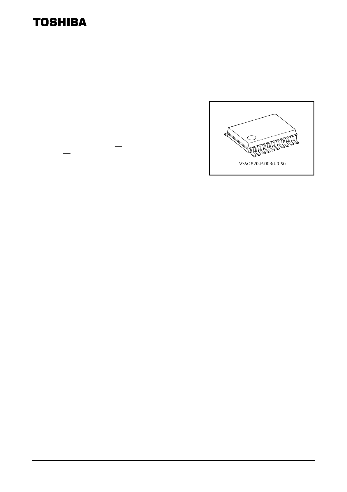
Package Dimensions
TC7MH573FK
Weight: 0.03 g (typ.)
7
2001-10-23
Page 8

TC7MH573FK
RESTRICTIONS ON PRODUCT USE
• The information contained herein is subject to change without notice.
• TOSHIBA is continually working to improve the quality and reliability of its products. Nevertheless, semiconductor
devices in general can malfunction or fail due to their inherent electrical sensitivity and vulnerability to physical
stress. It is the responsibility of the buyer, when utilizing TOSHIBA products, to comply with the standards of
safety in making a safe design for the entire system, and to avoid situations in which a malfunction or failure of
such TOSHIBA products could cause loss of human life, bodily injury or damage to property.
In developing your designs, please ensure that TOSHIBA products are used within specified operating ranges as
set forth in the most recent TOSHIBA products specifications. Also, please keep in mind the precautions and
conditions set forth in the “Handling Guide for Semiconductor Devices,” or “TOSHIBA Semiconductor Reliability
Handbook” etc.
• The TOSHIBA products listed in this document are intended for usage in general electronics applications
(computer, personal equipment, office equipment, measuring equipment, industrial robotics, domestic appliances,
etc.).These TOSHIBA products are neither intended nor warranted for usage in equipment that requires
extraordinarily high quality and/or reliability or a malfunction or failure of which may cause loss of human life or
bodily injury (“Unintended Usage”). Unintended Usage include atomic energy control instruments, airplane or
spaceship instruments, transportation instruments, traffic signal instruments, combustion control instruments,
medical instruments, all types of safety devices, etc.. Unintended Usage of TOSHIBA products listed in his
document shall be made at the customer’s own risk.
• The products described in this document shall not be used or embedded to any downstream products of which
manufacture, use and/or sale are prohibited under any applicable laws and regulations.
• The information contained herein is presented only as a guide for the applications of our products. No
responsibility is assumed by TOSHIBA for any infringements of patents or other rights of the third parties which
may result from its use. No license is granted by implication or otherwise under any patents or other rights of
TOSHIBA or the third parties.
20070701-EN
• Please contact your sales representative for product-by-product details in this document regarding RoHS
compatibility. Please use these products in this document in compliance with all applicable laws and regulations
that regulate the inclusion or use of controlled substances. Toshiba assumes no liability for damage or losses
occurring as a result of noncompliance with applicable laws and regulations.
8
2001-10-23
 Loading...