

Page 1
TC70/71
MICROMASTER™ – SYSTEM SUPERVISOR WITH POWER SUPPLY
MONITOR, W A TCHDOG AND BA TTER Y BACKUP
1
2
FEATURES
■ Maximum Functional Integration: Precision Power
Supply Monitor, Watchdog Timer, External RESET
Override, Threshold Detector and Battery Backup
Controller in an 8-Pin Package
■ Generates Power-on RESET and Guards Against
Unstable Processor Operation Resulting from
Power "Brown-out"
■ Automatically Halts and Restarts an Out-of-
Control Microprocessor
■ Output Can be Wire-ORed, or Hooked to Manual
RESET Pushbutton Switch
■ Watchdog Disable Pin for Easier Prototyping
(TC70)
■ Voltage Monitor for Power Fail or Low Battery
Warning (TC71)
■ Available in 8-Pin Plastic DIP or 8-Pin SOIC
Packages
■ Cost Effective
TYPICAL APPLICATIONS
■ All Microprocessor-based Systems
■ Test Equipment
■ Instrumentation
■ Set-Top Boxes
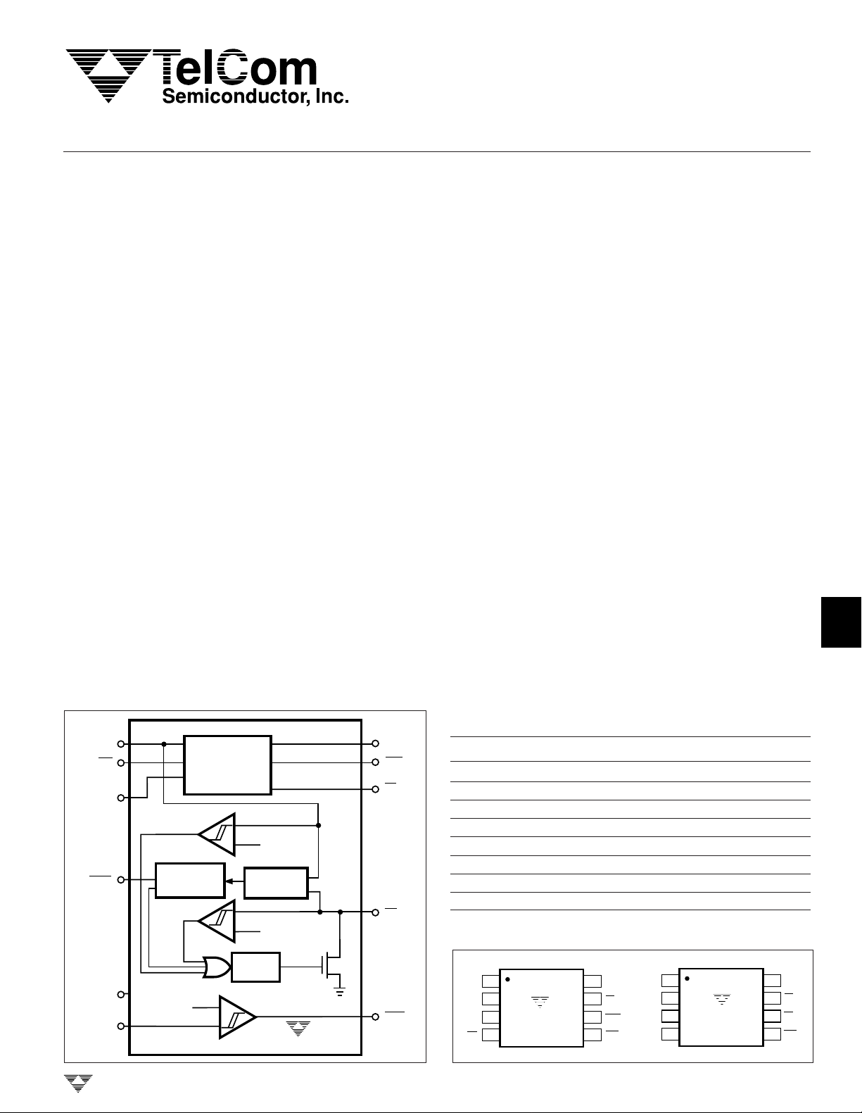
FUNCTIONAL BLOCK DIAGRAM
V
CC V
CEI
(TC70)
V
BATT
WDD
(TC70)
GND
TDI
(TC71)
WATCHDOG
V
REF3
TIMER
BATTERY
BACK-UP
CONTROL
DELAY
TIMER
V
REF1
∆V
DETECTOR
V
REF2
TC70/71
TELCOM SEMICONDUCTOR, INC.
CCO
CEO
(TC70)
PF
(TC71)
RS
TDO
(TC71)
GENERAL DESCRIPTION
The TC70/71 is a fully-integrated power supply monitor,
watchdog and battery backup circuit in a space-saving
8-pin package.
When power is initially applied, the TC70/71 holds the
processor in its reset state for a minimum of 500msec after
VCC is in tolerance to ensure stable system start-up. After
start-up, processor sanity is monitored by the on-board
watchdog circuit. The processor must provide periodic highto-low level transitions to the TC70/71 to verify proper
execution. Should the processor fail to supply this signal
within the specified timeout period, an out-of-control processor is indicated and the TC70/71 issues a momentary
processor reset as a result. The TC70 also features a
watchdog disable pin to facilitate system test and debug.
The output of the TC70/71 can be wire-ORed to a pushbutton switch (or electronic signal) to reset the processor.
When connected to a push-button switch, the TC70/71
provides contact debounce.
The integrated battery backup circuit on-board the TC70/
71 converts CMOS RAM into nonvolatile memory by first
write-protecting, then switching the VCC line of the RAM over
to an external battery.
The TC71 incorporates an additional 1.3V threshold
detector for power fail warning, low battery detection or to
monitor power supply voltages other than +5V.
ORDERING INFORMATION
Part No. Package Temp. Range
T
C70COA 8-Pin SOIC 0°C to +70°C
TC70CPA 8-Pin Plastic DIP 0°C to +70°C
TC70EOA 8-Pin SOIC – 40°C to +85°C
TC70EPA 8-Pin Plastic DIP – 40°C to +85°C
T
C71COA 8-Pin SOIC 0°C to +70°C
TC71CPA 8-Pin Plastic DIP 0°C to +70°C
TC71EOA 8-Pin SOIC – 40°C to +85°C
TC71EPA 8-Pin Plastic DIP – 40°C to +85°C
PIN CONFIGURATIONS (DIP and SOIC)
V
1
CCO
V
27
CC
GND
CEI
TC70
3
4
V
8
BATT
RS
6
WDD
5
CEO
V
1
CCO
V
27
CC
3
GND
4
TDI
TC71
TC70/71-1 11/18/96
V
8
BATT
RS
PF
6
5
TDO
5-7
3
4
5
6
7
8
Page 2
TC70/71
MICROMASTER™ – SYSTEM SUPERVISOR
WITH POWER SUPPL Y MONITOR, W A TCHDOG
AND BA TTER Y BACKUP
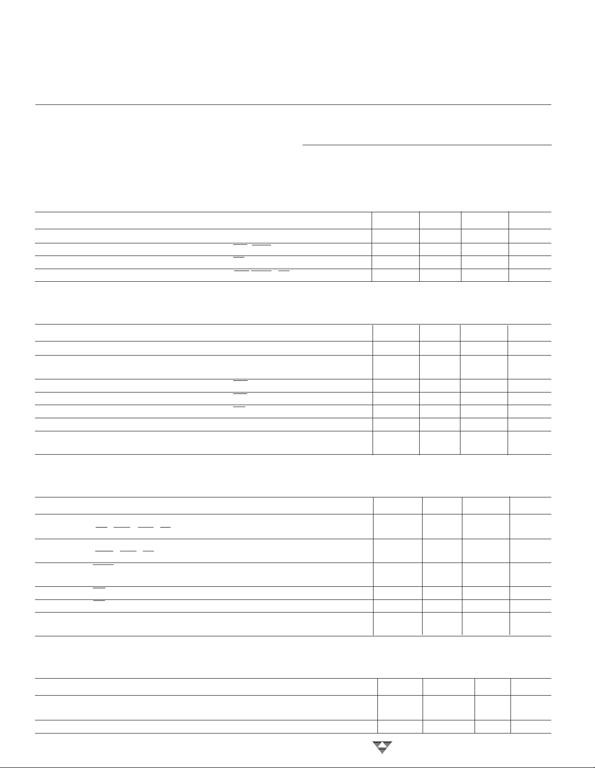
ABSOLUTE MAXIMUM RATINGS*
Voltage (Any Pin) with Respect to
Ground................................ GND – 0.3 to VCC + 0.3V
Operating Temperature Range ...............– 40°C to +85°C
ELECTRICAL CHARACTERISTICS: Recommended DC Operations: T
A
= T
MIN
to T
MAX,
Storage Temperature Range ................– 65°C to +150°C
Lead Temperature (Soldering, 10 sec) .................+300°C
*This is a stress rating only and functional operation of the device at these
or any other conditions above those indicated in the operational sections of
the specifications is not implied. Exposure to Absolute Maximum Rating
Conditions for extended periods may affect device reliability.
unless otherwise specified.
Symbol Parameter Test Conditions Min Typ Max Unit
V
CC
V
IH
V
IH
V
IL
Supply Voltage Note 1 4.5 5.0 5.5 V
Input HIGH Level CEI, WDD (Note 1) 2.5 — — V
Input HIGH Level RS (Note 1) 2.2 — — V
Input LOW Level CEI, WDD, RS (Note 1) — — 0.8 V
ELECTRICAL CHARACTERISTICS: DC: T
Symbol Parameter Test Conditions Min Typ Max Unit
I
CC1
I
CC2
I
IH
I
IL
I
IH
I
STBY
I
STBY
A
= T
MIN
to T
, VCC = 4.5V to 5.5V, unless otherwise specified.
MAX
Operating Current Notes 2, 3 — 5 6.5 mA
Operating Current in VCC = 0; V
= 2.8V; (Note 3) — 0.01 0.20 µA
BATT
Battery Backup Mode
Input Leakage CEI — 4 7 µA
Input Leakage CEI — 1 — µA
Input Leakage RS — 1 — µA
Battery Standby Current 5.5V > VCC > V
Battery Standby Current 5.5V > VCC > V
+ 0.2V – 1.0 — 0.02 µA
BATT
+ 0.2V – 0.1 — 0.02 µA
BATT
TA = 25°C
ELECTRICAL CHARACTERISTICS:
DC: Power Supply Monitor, EXT. RESET and Watchdog:
Symbol Parameter Test Conditions Min Typ Max Unit
I
OL
I
OH
WDD
I
V
STH
V
STL
V
CCTRIP
Output Current 0.4V VOL = 0.4V 2 5 — mA
(RS, TDO, CEO, PF Pins)
Output Current 2.4V VOH = 2.4V 2 3 — mA
(TDO, CEO, PF Pins)
WDD Input Current WDD = GND – 120 — — µA
WDD = V
RS Strobe (HIGH) Level Figure 3 (Note 1) VDD – 0.5 — — V
RS Strobe (LOW) Level Figure 3 (Note 1) 2.2 — VDD – 1.8 V
VCC Trip Point (Note 1) 0°C ≤ TA ≤ 70°C 4.25 — 4.49
– 40°C ≤ TA ≤ 85°C 4.20 4.49
CC
TA = T
MIN
to T
, VCC = 4.5V to 5.5V,
MAX
——25
unless otherwise specified.
ELECTRICAL CHARACTERISTICS:
DC: Battery Backup and Threshold Detector:
Symbol Parameter Test Conditions Min Typ Max Unit
V
V
5-8
OUT1
OUT2
V
Output Voltage I
CCO
V
in Battery Backup Mode
OUT
TA = T
= 1mA VCC – 0.3 VCC – 0.1 — V
OUT
I
= 50mA VCC – 0.5 VCC – 0.20 —
OUT
I
= 250µA, VCC < V
OUT
MIN
to T
, VCC = 4.5V to 5.5V, unless otherwise specified.
MAX
BATT
– 0.2, V
BATT
= 2.8V
V
BATT
– 0.1 V
BATT
– 0.02
— V
TELCOM SEMICONDUCTOR, INC.
Page 3
MICROMASTER™ – SYSTEM SUPERVISOR
WITH POWER SUPPL Y MONITOR, W A TCHDOG
AND BA TTER Y BACKUP
TC70/71
ELECTRICAL CHARACTERISTICS: (Cont.)
DC: Battery Backup and Threshold Detector:
Symbol Parameter Test Conditions Min Typ Max Unit
I
OUT1
I
OUT2
V
SW
V
HYST
VOH
CEO
V
TDI
I
TDI
V
TDI (HYST)
V
Output Current VCC = 4.5V, V
CCO
V
Output Current in V
CCO
Battery Backup Mode V
Battery Switchover Threshold —
(VCC Falling)
Battery Switchover Hysteresis — 20 — mV
CEO Output Voltage in VCC < V
Battery Backup Mode IOH = 10µA
Threshold Detector Trip Voltage 1.2 — 1.4 V
Threshold Detector Input Current TA = 25°C –25 — +25 nA
Threshold Detector Hysteresis — 10 — mV
CCO
BATT
TA = T
= V
= 2.8V
BATT
to T
MIN
CCO
– 0.3V 500 — — µA
BATT
– 0.2, V
, VCC = 4.5V to 5.5V, unless otherwise specified.
MAX
= 3.5V 50 100 — mA
V
= 2.8V V
BATT
– 0.01
BATT
– 0.2 — — V
BATT
—V
1
2
3
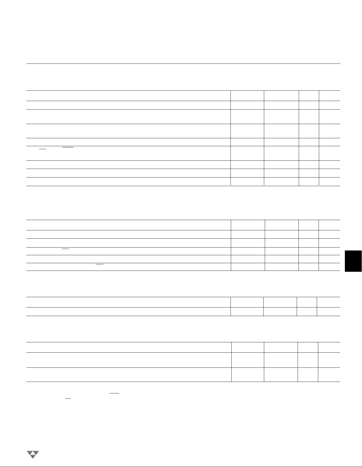
ELECTRICAL CHARACTERISTICS: AC: Power Supply Monitor, EXT. RESET and Watchdog:
Symbol Parameter Test Conditions Min Typ Max Unit
t
PBH
t
RST
t
ST
t
TD
t
RPD
PB Hold Time Figure 4 (Note 4) 20 — — msec
Reset Active Time Figure 6 500 — 900 msec
RS STROBE Pulsewidth Figure 3 500 — — nsec
Watchdog Timeout Period Figure 3 500 700 900 msec
VCC Detect to RS LOW Figure 6 — — 100 nsec
TA = T
MIN
specified.
to T
, VCC = 4.5V to 5.5V, unless otherwise
MAX
ELECTRICAL CHARACTERISTICS:
AC: Battery Backup and Threshold Detector:
Symbol Parameter Test Conditions Min Typ Max Unit
t
PD
CE Propagational Delay Figure 7 — — 50 nsec
TA = T
MIN
to T
, VCC = 4.5V to 5.5V, unless otherwise specified.
MAX
ELECTRICAL CHARACTERISTICS:
AC:
TA = T
Symbol Parameter Test Conditions Min Typ Max Unit
t
F
t
R
NOTES: 1. All voltages referenced to ground.
to T
MIN
VCC Fall Time From Figure 5 (Note 1) 10 — — µsec
4.25V to 3.0V
VCC Rise Time From Figure 5 (Note 1) 0 — — µsec
3.0V to 4.25V
2. No output load.
3 Measured with V
4. The RS output must be held low for a minimum of 20msec to guarantee a reset.
MAX
.
CCO
and CEO open.
4
5
6
7
TELCOM SEMICONDUCTOR, INC.
8
5-9
Page 4

TC70
TC71
PIN DESCRIPTION
Pin No Pin No
(TC70) (TC71) Symbol Description
11V
22 VCCV
3 3 GND GND Input. Ground.
4 – CEI Chip enable input. Chip enable to static RAM or other device to be battery
– 4 TDI Threshold detector input. When the voltage on threshold detector input (TDI) is
5 – CEO Chip enable output. This line goes low only when CEI is low and VCC is above
– 5 TDO Threshold detector output. TDO goes low when TDI is less than 1.3V and VCC is
6 – WDD Watchdog disable input. Grounding this line disables the watchdog timer (no
– 6 PF Power fail output. This line goes low when V
7 7 RS RESET/STORE (Bidirectional). An open drain with pull-up (in output mode) that
88V
CCO
BATT
V
CC
Connect to VCC if V
CC
backed-up. Connect to ground if V
less than 1.3V, threshold detector output (TDO) goes low.
the RESET threshold.
greater than V
V
BATT
RESET pulses are generated after the watchdog timer times out). This input is
provided to facilitate system debug. This input is internally pulled-up and can be
left open, or tied to VCC for normal watchdog operation.
to write-protect the external device to be battery backed.
goes active if:
1. V
2. If pulled low by an external electronic signal or switch closure
3. If the watchdog is not strobed within the minimum watchdog timeout period
4. During power-up and power down
In the input mode, RS is a negative edge triggered input that resets the
watchdog timer when pulled to ground through a 10kΩ, 5% tolerance resistor.
Backup battery input. Connect to ground if battery backup is not used.
MICROMASTER™ – SYSTEM SUPERVISOR
WITH POWER SUPPL Y MONITOR, W A TCHDOG
AND BA TTER Y BACKUP
Output. The higher of VCC or V
and V
BATT
Input. +5V power supply.
. (The threshold detector is turned off when VCC is less than
.
CC
BATT
falls below 4.5V nominal
CCO
is internally switched to this output.
BATT
are not used.
is not used.
CCO
is below 4.5V nominal. It is used
CC
DETAILED DESCRIPTION
Precision Power Supply Monitor
The RS pin is immediately driven low any time VCC is
below 4.5V nominal. The processor is held in its reset state
during power-up and power-down. RS remains low for a
minimum of 500msec after VCC is within tolerance to allow
the power supply and processor to stabilize.
Watchdog Timer
The processor drives the RS pin with an input/output
(I/O) line in series with a voltage divider to VDD. Pulling the
bottom of this divider low results in an internal voltage
change (strobe) sufficient to reset the watchdog timer, but
above the VIL input threshold of the processor RESET input.
The processor must continuously apply strobes in this
manner within a set period to verify proper software execution. A momentary reset (500msec minimum) is generated
if a hardware or software failure keeps RS from being
5-10
strobed within the watchdog timeout period. This action
typically initiates the processor's power-up routine. If the
interruption persists, new reset pulses are generated each
timeout period until RS is strobed. The timeout period is
typically 700msec.
It is often difficult to debug a system while the watchdog
is continuously generating reset pulses. For example, the
watchdog must be disabled when the system is operated
with an in-circuit emulator (ICE). The watchdog disable input
(TC70) is provided for system debugging, (or if the watchdog
timer on-board the processor is to be used). Grounding
WDD disables the watchdog (all other functions remain
intact). For normal watchdog operation, WDD can be tied to
VDD.
The software routine that drives the RS strobe must be
in a section of the program that executes frequently enough
so the time between toggles is less than one watchdog
timeout period. The strobe signal can be derived from
microprocessor address, data and/or control signals. Typical circuit examples are shown in Figure 1.
TELCOM SEMICONDUCTOR, INC.
Page 5

MICROMASTER™ – SYSTEM SUPERVISOR
WITH POWER SUPPL Y MONITOR, W A TCHDOG
AND BA TTER Y BACKUP
1
TC70
TC71
Resistor Value Selection
The values of R1 and R2 must be chosen to ensure a
valid low strobe level (V
line is low. The use of 10kΩ, ±5% tolerance resistors are
recommended. These values result in a nominal strobe level
of 2.83V on RS (min/max of 2.43V/3.24V, assuming
V
= 5.0V ±10%). Other resistor values can be used, so
DD
long as the additive tolerances of the power supply and
resistor values result in a strobe that falls within V
V
under all additive tolerance conditions.
STL
) on RS when the processor I/O
STL
STH
and
External Override Reset Control
A built-in debounce circuit allows a pushbutton switch
(or other electronic reset signal) to be wire-ORed to RS as
an external reset override (Figure 4). The external reset
signal is required to be an active low signal of at least
20msec in duration. Internally, this input is timed to provide
a minimum reset pulse width output of 500msec.
Threshold Detector
The TC71 issues a low-true output on the TDO pin any
time the TDI pin is less than 1.3V and VCC is greater than
V
. The voltage to be monitored is connected to the TDI
BATT
input through a simple resistor divider. The threshold detector can be used to generate an early power fail warning if the
unregulated DC input to the +5V regulator is available for
monitoring.
data corruption during power up and power down. The
battery switchover circuit compares VCC to the V
and connects VCCO to whichever is higher. Switchover
(VSW) occurs when VCC is 10mV below V
and when VCC is 10mV more than V
battery switchover comparator has 20mV of hysteresis to
prevent switch chattering if VCC falls very slowly.
BATT
as VCC falls,
BATT
as VCC rises. The
BATT
input
Integrated Battery Backup (TC71)
The TC71 differs from the TC70 in that it has a Power
Fail (PF) output instead of a gated chip enable (CEI, CEO).
PF must be externally gated with the decode for the CMOS
RAM or other device to be battery-backed. (Many CMOS
RAMs have both CE and CE enables. In this case, the PF
output can be connected directly to the CE input of the RAM).
PF is high as long as VCC is greater than 4.5V nominal.
When VCC falls below 4.5V nominal, PF is driven low.
Battery switchover for the TC71 is otherwise identical to that
of the TC70.
Supply Monitor Noise Sensitivity
The TC70/71 is optimized for fast response to negativegoing changes in VDD. Systems with an inordinate amount
of electrical noise on VDD (such as systems using relays),
may require a 0.1µF bypass capacitor to reduce detection
sensitivity. This capacitor should be installed as close to the
TC70/71 as possible to keep the capacitor lead length short.
2
3
4
5
Integrated Battery Backup (TC70)
The CEO line (TC70) drives the CE input of a CMOS
RAM or other device to be battery-backed. CEO follows CEI
as long as VCC is greater than 4.5V nominal. If VCC falls
below 4.5V nominal, CEO is driven to the potential of VCCO
thus write protecting the RAM and preventing accidental
VCCO
CEO
CEI
RS
Figure 1. TC70 Typical Application
+5V
+3V L
I
BATTERY
WDD
V
CC
V
BATT
GND
TC70
TYPICAL APPLICATIONS
Figure 1 shows a full feature implementation of the
TC70; Figure 2 shows the TC71. Resistors R1 and R2 of
Figure 2 set the trip point voltage for the early power fail
warning circuit using the TC71 threshold detector.
V
CC
CMOS
RAM
CE
+5V
R1
10K
ADDRESS
DECODER
R2
13K
RESET
ADDRESS
I/O
RESET
PROCESSOR
6
7
8
TELCOM SEMICONDUCTOR, INC.
5-11
Page 6

TC70
TC71
MICROMASTER™ – SYSTEM SUPERVISOR
WITH POWER SUPPL Y MONITOR, W A TCHDOG
AND BA TTER Y BACKUP
REGULATOR
R3
R4
FILTER CAP
TC55RP
RECTIFIER
V
CC
3V L
I
WDD
V
CC
TDI
V
BATT
GND
AC I
N
VCCO
PF
V
CE
CC
CE
TC71
TDO
V
R3
10K
RS
Figure 2. TC71 Typical Application
CC
RESET
CMOS
RAM
ADDRESS
DECODER
R4
13K
ADDRESS
NMI
I/O
RESET
PROCESSOR
t
ST
RS
V
(MIN)
STH
V
(MAX)
STL
(MIN)
V
STL
t
TD
Note: t
will keep the watchdog timer from forcing RS LOW.
(A
is the maximum elapsed time between strobes which
TD
STROBE
is defined as a high-to-low transition from V
Figure 3. Watchdog Strobe
STH
to V
STL
PB CLOSED
t
RS
)
.
PBH
V
IL
PB OPEN
t
RST
V
IH
Figure 4. RS Override Reset
5-12
TELCOM SEMICONDUCTOR, INC.
Page 7

MICROMASTER™ – SYSTEM SUPERVISOR
WITH POWER SUPPL Y MONITOR, W A TCHDOG
AND BA TTER Y BACKUP
1
TC70
TC71
V
CEI
t
R
t
F
CC
4.25V
3.0V
Figure 5. Power Up/Down Slew Rate Figure 6. Power Up/Down Reset Timing
V
IH
V
CC
4.25V
CEI
RS
V
t
RPD
V
IL
OL
t
RST
2
3
V
OH
4
5
V
BATT- 0.2V
CEO
V
CC
V
IH
t
PD
4.25V
3.0V
t
R
Figure 7. Battery Backup (Power-Up)
CEO
V
t
PD
CC
Figure 8. Battery Backup (Power-Down)
4.25V
3.0V
t
F
V
BATT-0.2V
6
7
8
TELCOM SEMICONDUCTOR, INC.
5-13
 Loading...