

Datasheet TC7107CPL, TC7107ARIJL, TC7107ARIPL, TC7107ARCPL, TC7107ARCLW Datasheet (TelCom Semiconductor)
...Page 1
3-183
TELCOM SEMICONDUCTOR, INC.
7
6
5
4
3
1
2
8
TC7106
TC7106A
TC7107
TC7107A
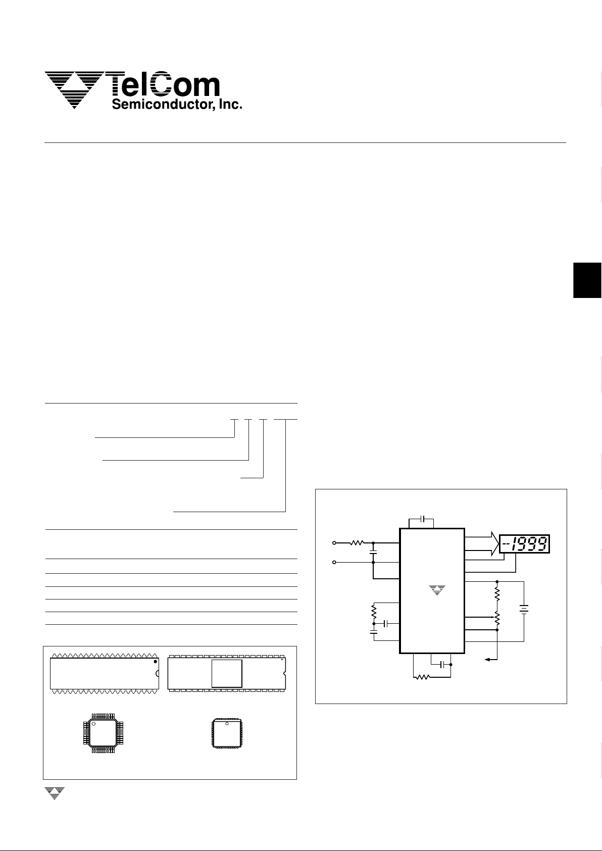
Figure 1. TC7106/A/7/A Typical Operating Circuit
AVAILABLE PACKAGES
40-Pin Plastic DIP
40-Pin CERDIP
44-Pin Plastic Quad Flat
Package Formed Leads
44-Pin Plastic Chip
Carrier PLCC
V
REF
+
TC7106/A
TC7107/A
9V
V
REF
33
34
24kΩ
1kΩ
29
36
39 38 40
0.47µF
0.1µF
V
–
1
OSC
3
OSC
2
OSC
TO ANALOG
COMMON (PIN 32)
3 CONVERSIONS/SEC
200mV FULL SCALE
C
OSC
100kΩ
47kΩ
0.22µF
C
REF
–
C
REF
+
V
IN
+
V
IN
–
ANALOG
COMMON
V
INT
V
BUFF
C
AZ
20
21
SEGMENT
DRIVE
2–19
22–25
POL
BP
V
+
MINUS SIGN
BACKPLANE
DRIVE
28
R
OSC
100pF
LCD DISPLAY (TC7106/A) OR
COMMON ANODE LED
DISPLAY (TC7107/A)
27
100mV
1
26
35
V
REF
–
+
31
0.01µF
ANALOG
INPUT
+
–
1MΩ
30
32
ORDERING INFORMATION
PART CODE TC710X X X XXX
6 = LCD
7 = LED
A or blank*
R (reversed pins) or blank (CPL pkg only)
* "A" parts have an improved reference TC
Package Code (see below):
}
Package Temperature
Code Package Pin Layout Range
CKW 44-Pin PQFP Formed Leads 0°C to +70°C
CLW 44-Pin PLCC — 0°C to +70°C
CPL 40-Pin PDIP Normal 0°C to +70°C
IPL 40-Pin PDIP Normal – 25°C to +85°C
IJL 40-Pin CerDIP Normal – 25°C to +85°C
GENERAL DESCRIPTION
The TC7106A and TC7107A 3-1/2 digit direct-display
drive analog-to-digital converters allow existing 7106/7107
based systems to be upgraded. Each device has a precision reference with a 20ppm/°C max temperature coefficient. This represents a 4 to 7 times improvement over
similar 3-1/2 digit converters. Existing 7106 and 7107 based
systems may be upgraded without changing external passive component values. The TC7107A drives common
anode light emitting diode (LED) displays directly with 8mA
per segment. A low-cost, high-resolution indicating meter
requires only a display, four resistors, and four capacitors.
The TC7106A low power drain and 9V battery operation
make it suitable for portable applications.
The TC7106A/TC7107A reduces linearity error to less
than 1 count. Rollover error – the difference in readings for
equal magnitude but opposite polarity input signals – is
below ±1 count. High impedance differential inputs offer
1pA leakage current and a 1012Ω input impedance. The
differential reference input allows ratiometric measurements
for ohms or bridge transducer measurements. The
15µV
P–P
noise performance guarantees a “rock solid” reading. The auto-zero cycle guarantees a zero display reading with a zero-volts input.
FEATURES
■ Internal Reference with Low Temperature Drift
TC7106/7 ....................................... 80ppm/°C Typical
TC7106A/7A..................................20ppm/°C Typical
■ Drives LCD (TC7106) or LED (TC7107) Display
Directly
■ Guaranteed Zero Reading With Zero Input
■ Low Noise for Stable Display
■ Auto-Zero Cycle Eliminates Need for Zero
Adjustment
■ True Polarity Indication for Precision Null
Applications
■ Convenient 9 V Battery Operation (TC7106A)
■ High Impedance CMOS Differential Inputs.... 1012Ω
■ Differential Reference Inputs Simplify Ratiometric
Measurements
■ Low Power Operation..................................... 10mW
3-1/2 DIGIT A/D CONVERTERS
TC7106/6A/7/7A-7 11/4/96
Page 2

3-184
TELCOM SEMICONDUCTOR, INC.
ELECTRICAL CHARACTERISTICS (Note 3)
TC7106/A & TC7107/A
Parameters Test Conditions Min Typ Max Unit
Zero Input Reading VIN = 0.0 V – 000.0 ±000.0 +000.0 Digital
Full-Scale = 200.0mV Reading
Ratiometric Reading VIN = V
REF
999 999/1000 1000 Digital
V
REF
= 100 mV Reading
Roll-Over Error (Difference in V
–
IN
= +V
+
IN
≅ 200mV – 1 ±0.2 +1 Counts
Reading for Equal Positive and
Negative Reading Near Full-Scale)
Linearity (Max. Deviation From Full-Scale = 200mV – 1 ±0.2 +1 Counts
Best Straight Line Fit) or Full-Scale = 2.000 V
Common-Mode V
CM
= ±1V, VIN = 0V, — 50 — µV/V
Rejection Ratio (Note 4) Full Scale = 200.0 mV
Noise (Pk – Pk Value Not V
IN
= 0 V — 15 — µV
Exceeded 95% of Time) Full-Scale = 200.0mV
Leakage Current @ Input VIN = 0 V — 1 10 pA
Zero Reading Drift VIN = 0 V
“C” Device = 0°C to +70°C — 0.2 1 µV/°C
VIN = 0 V
“I” Device = – 25°C to +85°C — 1.0 2 µV/°C
Scale Factor VIN = 199.0mV,
Temperature Coefficient “C” Device = 0°C to +70°C — 1 5 ppm/°C
(Ext. Ref = 0ppm°C)
V
IN
= 199.0mV — — 20 ppm/°C
“I” Device = – 25°C to +85°C
Supply Current (Does Not VIN = 0 — 0.8 1.8 mA
Include LED Current For TC7107/A)
ABSOLUTE MAXIMUM RATINGS*
TC7106A
Supply Voltage (V+ to V–)...........................................15 V
Analog Input Voltage (either input) (Note 1)......... V+ to V
–
Reference Input Voltage (either input) ................. V+ to V
–
Clock Input ........................................................ Test to V
+
Package Power Dissipation (Note 2) (TA ≤ 70°C)
CerDIP..............................................................2.29W
Plastic DIP ........................................................1.23W
PLCC ................................................................1.23W
PQFP................................................................1.00W
Operating Temperature
“C” Devices............................................ 0°C to +70°C
“I” Devices ........................................– 25°C to +85°C
Storage Temperature ............................– 65°C to +150°C
Lead Temperature (Soldering, 60 sec) ...................300°C
TC7107A
Supply Voltage
V
+
................................................................................................ +6 V
V
–
............................................................................................... – 9 V
Analog Input Voltage (either input) (Note 1)......... V+ to V
–
Reference Input Voltage (either input) ................. V+ to V
–
Clock Input ....................................................... GND to V
+
Power Dissipation (Note 2) (TA ≤ 70°C)
40-Pin CerDIP Package ...................................2.29W
40-Pin Plastic DIP.............................................1.23W
44-Pin PLCC.....................................................1.23W
44-Pin PQFP ....................................................1.00W
Operating Temperature
“C” Devices............................................ 0°C to +70°C
“I” Devices ........................................– 25°C to +85°C
Storage Temperature ............................– 65°C to +150°C
Lead Temperature (Soldering, 10 sec) .................+300°C
*Static-sensitive device. Unused devices must be stored in conductive
material. Protect devices from static discharge and static fields. Stresses
above those listed under Absolute Maximum Ratings may cause permanent damage to the device. These are stress ratings only and functional
operation of the device at these or any other conditions above those
indicated in the operational sections of the specifications is not implied.
Exposure to Absolute Maximum Rating Conditions for extended periods
may affect device reliability.
TC7106
TC7106A
TC7107
TC7107A
3-1/2 DIGIT A/D CONVERTERS
Page 3

3-185
TELCOM SEMICONDUCTOR, INC.
7
6
5
4
3
1
2
8
ELECTRICAL CHARACTERISTICS (Cont.) (Note 3)
TC7106/A & TC7107/A
Parameters Test Conditions Min Typ Max Unit
Analog Common Voltage 25kΩ Between Common 2.7 3.05 3.35 V
(With Respect to Pos. Supply) and Pos. Supply
Temp. Coeff. of 25kΩ Between Common
Analog Common and Pos. Supply
(With Respect 0°C ≤ TA ≤ +70°C 7106A/7A 20 50 ppm/°C
to Pos. Supply) ("C", Commercial Temp. Range Devices) 7106/7 80 — ppm/°C
Temp. Coeff. of 25kΩ Between Common
Analog Common and Pos. Supply
(With Respect – 25°C ≤ T
A
≤ 85°C — — 75 ppm/°C
to Pos. Supply) (“I,” Industrial Temp. Range Devices)
TC7106A ONLY Pk – Pk V
+
to V– = 9V 4 5 6 V
Segment Drive Voltage (Note 5)
TC7106A ONLY Pk – Pk V+ to V– = 9V 4 5 6 V
Backplane Drive Voltage (Note 5)
TC7107A ONLY V+ = 5.0V 5 8.0 — mA
Segment Sinking Current (Except Pin 19) Segment Voltage = 3V
TC7107A ONLY V+ = 5.0V 10 16 — mA
Segment Sinking Current (Pin 19) Segment Voltage = 3V
NOTES: 1. Input voltages may exceed the supply voltages provided the input current is limited to ±100µA.
2. Dissipation rating assumes device is mounted with all leads soldered to printed circuit board.
3. Unless otherwise noted, specifications apply to both the TC7106/A and TC7107/A at TA = 25°C, f
CLOCK
= 48 kHz. Parts are tested in the
circuit of Figure 1.
4. Refer to “Differential Input” discussion.
5. Backplane drive is in phase with segment drive for “OFF” segment, 180° out of phase for “ON” segment. Frequency is 20 times
conversion rate. Average DC component is less than 50mV.
TC7106
TC7106A
TC7107
TC7107A
3-1/2 DIGIT A/D CONVERTERS
Page 4
3-186
TELCOM SEMICONDUCTOR, INC.
TC7106
TC7106A
TC7107
TC7107A
3-1/2 DIGIT A/D CONVERTERS
PIN CONFIGURATIONS
TC7106ACPL
TC7107AIPL
1
2
3
4
OSC
1
5
6
7
8
9
10
11
12
TEST
V
ANALOG
COMMON
C
AZ
V
+
D
NORMAL PIN
CONFIGURATION
13
14
15
16
17
18
19
20
40
39
38
37
36
35
34
33
32
31
30
29
28
27
26
25
24
23
22
21
2
C
2
B
2
A
2
F
2
E
2
D
3
B
3
F
3
E
3
AB
4
(MINUS SIGN)
10's
100's
1000's
(7106A/7107A)
100's
OSC
2
OSC
3
+
REF
V
–
REF
C
+
REF
C
–
REF
V
+
IN
V
–
IN
V
BUFF
V
INT
V
–
G
C
A
G
BP/GND
POL
3
3
3
2
TC7106AIJL
TC7107AIJL
1
2
3
4
5
6
7
8
9
10
11
12
13
14
15
16
17
18
19
20
100's
1000's
100's
REVERSE PIN
CONFIGURATION
40
39
38
37
36
35
34
33
32
31
30
29
28
27
26
25
24
23
22
21
D
1
C
1
B
1
A
1
F
1
G
1
E
1
1's
V
+
D
2
C
2
B
2
A
2
F
2
E
2
D
3
B
3
F
3
E
3
AB
4
(MINUS SIGN)
POL
D
1
C
1
B
1
A
1
F
1
G
1
E
1
1's
10's
OSC
TEST
V
ANALOG
COMMON
C
AZ
OSC
2
OSC
+
REF
V
–
REF
C
+
REF
C
–
REF
V
+
IN
V
–
IN
V
BUFF
V
INT
V
–
G
C
A
G
BP/GND
3
3
3
2
(7106A/7107A)
3
1
27
26
25
24
23
7
8
9
10
11
NC
G
2
NC
NC
TEST
OSC
3
NC
OSC
2
OSC
1
V
+
D
1
C
1
B
1
12 13 14 15 16 17 18 19 20 21 22
38 37 36 35 34
REF HI
A
1F1
TC7106ACKW
TC7107ACKW
(FLAT PACKAGE)
394041424344
28
29
30
31
32
33
6
5
4
3
2
1
REF LO
C
REFCREF
COM
IN HI
IN LO
A/Z
BUFF
INT
V
–
G
1E1D2C2B2A2F2E2D3
C
3
A
3
G
3
BP/GND
POL
AB
4
E
3
F
3
B
3
33
32
31
30
29
13
14
15
16
17
REF LO
C
REF
F
1
G
1
E
1
D
2
C
2
NC
B
2
A
2
F
2
E
2
D
3
18 19 20 21 22 23 24 25 26 27 28
44 43 42 41 40
A
1
B
3F3
TC7106ACLW
TC7107ACLW
(PLCC)
123456
34
35
36
37
38
39
12
11
10
9
8
7
B1C1D1V+NC
OSC1OSC2OSC3TEST
REF HI
E
3AB4
POL
NC
BP/GND
G
3A3C3G2
C
REF
COMMON
IN HI
NC
IN LO
A/Z
BUFF
INT
V
–
Page 5

3-187
TELCOM SEMICONDUCTOR, INC.
7
6
5
4
3
1
2
8
PIN DESCRIPTION
Pin No. Pin No.
40-Pin PDIP 40-Pin PDIP
(Normal) (Reverse) Symbol Description
1 (40) V
+
Positive supply voltage.
2 (39) D
1
Activates the D section of the units display.
3 (38) C
1
Activates the C section of the units display.
4 (37) B
1
Activates the B section of the units display.
5 (36) A
1
Activates the A section of the units display.
6 (35) F
1
Activates the F section of the units display.
7 (34) G
1
Activates the G section of the units display.
8 (33) E
1
Activates the E section of the units display.
9 (32) D
2
Activates the D section of the tens display.
10 (31) C
2
Activates the C section of the tens display.
11 (30) B
2
Activates the B section of the tens display.
12 (29) A
2
Activates the A section of the tens display.
13 (28) F
2
Activates the F section of the tens display.
14 (27) E
2
Activates the E section of the tens display.
15 (26) D
3
Activates the D section of the hundreds display.
16 (25) B
3
Activates the B section of the hundreds display.
17 (24) F
3
Activates the F section of the hundreds display.
18 (23) E
3
Activates the E section of the hundreds display.
19 (22) AB
4
Activates both halves of the 1 in the thousands display.
20 (21) POL Activates the negative polarity display.
21 (20) BP LCD Backplane drive output (TC7106A).
Digital ground (TC7107A).
22 (19) G
3
Activates the G section of the hundreds display.
23 (18) A
3
Activates the A section of the hundreds display.
24 (17) C
3
Activates the C section of the hundreds display.
25 (16) G
2
Activates the G section of the tens display.
26 (15) V
–
Negative power supply voltage.
27 (14) V
INT
Integrator output. Connection point for integration capacitor. See
INTEGRATING CAPACITOR section for more details
28 (13) V
BUFF
Integration resistor connection. Use a 47kΩ resistor for a 200mV full-
scale range and a 470kΩ resistor for 2V full-scale range.
29 (12) C
AZ
The size of the auto-zero capacitor influences system noise. Use a
0.47µF capacitor for 200mV full scale, and a 0.047µF capacitor for
2V full scale. See Paragraph on AUTO-ZERO CAPACITOR for more
details.
30 (11) V
–
IN
The analog LOW input is connected to this pin.
31 (10) V
+
IN
The analog HIGH input signal is connected to this pin.
32 (9) ANALOG This pin is primarily used to set the analog common-mode voltage
for battery operation or in systems where the input signal is
referenced to the power supply. It also acts as a reference voltage
source. See paragraph on ANALOG COMMON for more details.
33 (8) C
–
REF
See pin 34.
COMMON
GND
TC7106
TC7106A
TC7107
TC7107A
3-1/2 DIGIT A/D CONVERTERS
Page 6
3-188
TELCOM SEMICONDUCTOR, INC.
TC7106
TC7106A
TC7107
TC7107A
3-1/2 DIGIT A/D CONVERTERS
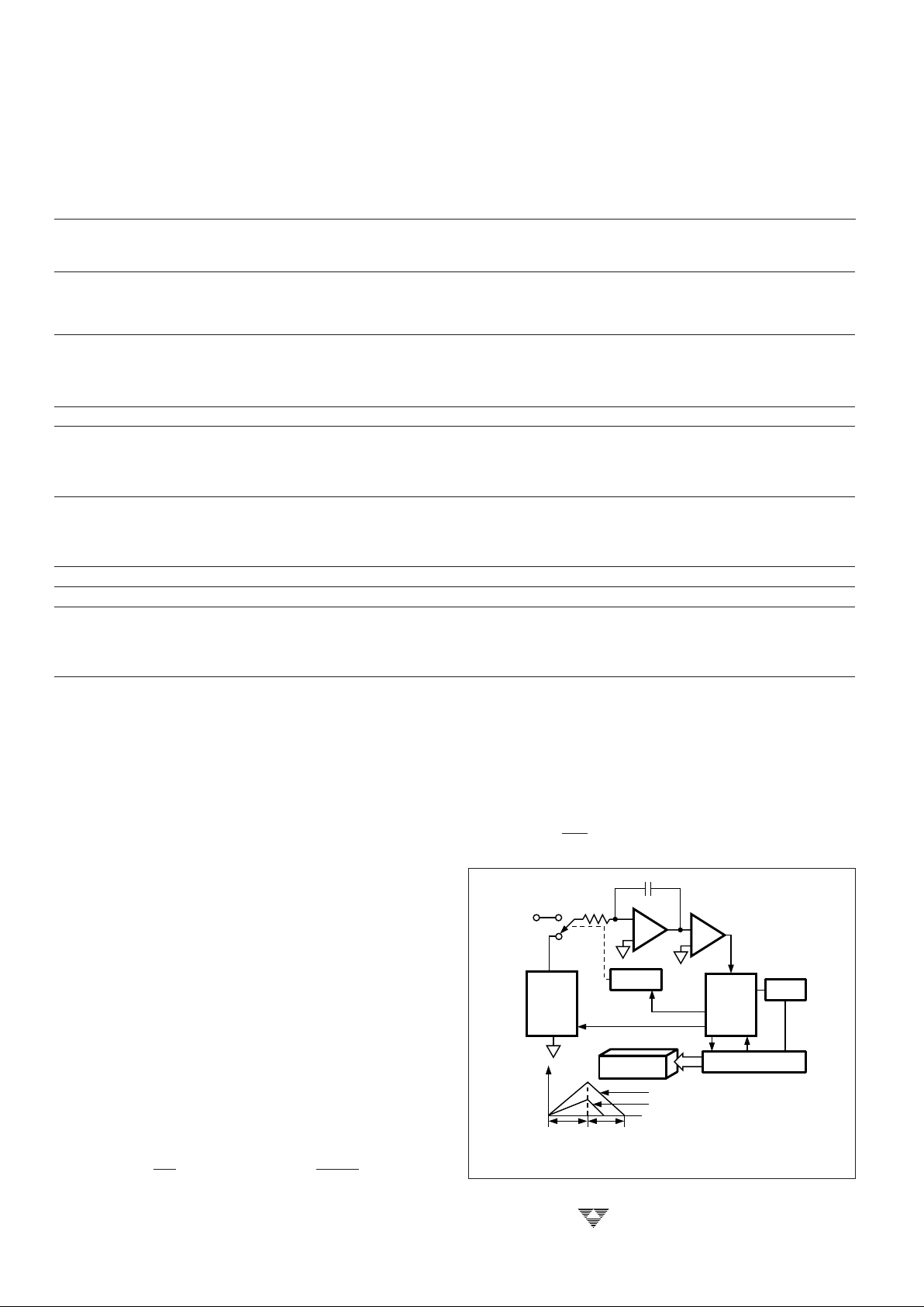
GENERAL THEORY OF OPERATION
DUAL SLOPE CONVERSION PRINCIPLES
(All Pin Designations Refer to the 40-Pin DIP)
The TC7106A and TC7107A are dual slope, integrating
analog-to-digital converters. An understanding of the dual
slope conversion technique will aid in following the detailed
operation theory.
The conventional dual slope converter measurement
cycle has two distinct phases:
• Input Signal Integration
• Reference Voltage Integration (Deintegration)
The input signal being converted is integrated for a fixed
time period (TSI). Time is measured by counting clock
pulses. An opposite polarity constant reference voltage is
then integrated until the integrator output voltage returns to
zero. The reference integration time is directly proportional
to the input signal (TRI). (Figure 2A).
In a simple dual slope converter a complete conversion
requires the integrator output to “ramp-up” and “rampdown.”
A simple mathematical equation relates the input signal,
reference voltage and integration time:
VIN(t)dt =
Figure 2A. Basic Dual Slope Converter
1
RC
∫
T
SI
VRT
RI
RC
0
where:
VR = Reference Voltage
TSI = Signal Integration Time (Fixed)
TRI = Reference Voltage Integration Time (Variable)
For a constant VIN:
VIN = V
R
T
RI
T
SI
+
–
REF
VOLTAGE
ANALOG
INPUT
SIGNAL
+
–
DISPLAY
SWITCH
DRIVER
CONTROL
LOGIC
INTEGRATOR
OUTPUT
CLOCK
COUNTER
POLARITY CONTROL
PHASE
CONTROL
V
IN
V
IN
V
FULL SCALE
1/2 V
FULL SCALE
VARIABLE
REFERENCE
INTEGRATE
TIME
FIXED
SIGNAL
INTEGRATE
TIME
INTEGRATOR
C
COMPARATOR
≈
≈
+/–
PIN DESCRIPTION (Cont.)
Pin No. Pin No.
40-Pin PDIP 40-Pin PDIP
(Normal) (Reverse) Symbol Description
34 (7) C
+
REF
A 0.1µF capacitor is used in most applications. If a large commonmode voltage exists (for example, the V
–
IN
pin is not at analog
common), and a 200mV scale is used, a 1µF capacitor is recommended and will hold the roll-over error to 0.5 count.
35 (6) V
–
REF
See pin 36.
36 (5) V
+
REF
The analog input required to generate a full-scale output (1999
counts). Place 100mV between pins 35 and 36 for 199.9mV
full-scale. Place 1V between pins 35 and 36 for 2V full scale. See
paragraph on REFERENCE VOLTAGE.
37 (4) Test Lamp test. When pulled HIGH (to V
+
) all segments will be turned on
and the display should read –1888. It may also be used as a negative
supply for externally-generated decimal points. See paragraph under
TEST for additional information.
38 (3) OSC
3
See pin 40.
39 (2) OSC
2
See pin 40.
40 (1) OSC
1
Pins 40, 39, 38 make up the oscillator section. For a 48kHz clock
(3 readings per section), connect pin 40 to the junction of a 100kΩ
resistor and a 100pF capacitor. The 100kΩ resistor is tied to pin 39
and the 100pF capacitor is tied to pin 38.
Page 7

3-189
TELCOM SEMICONDUCTOR, INC.
7
6
5
4
3
1
2
8
The dual slope converter accuracy is unrelated to the
integrating resistor and capacitor values as long as they are
stable during a measurement cycle. An inherent benefit is
noise immunity. Noise spikes are integrated or averaged to
zero during the integration periods. Integrating ADCs are
immune to the large conversion errors that plague successive approximation converters in high-noise environments.
Interfering signals with frequency components at multiples
of the averaging period will be attenuated. Integrating ADCs
commonly operate with the signal integration period set to a
multiple of the 50/60 Hz power line period. (Figure 2B)
Figure 2B. Normal-Mode Rejection of Dual Slope Converter
ANALOG SECTION
In addition to the basic signal integrate and deintegrate
cycles discussed, the circuit incorporates an auto-zero
cycle. This cycle removes buffer amplifier, integrator, and
comparator offset voltage error terms from the conversion.
A true digital zero reading results without adjusting external
potentiometers. A complete conversion consists of three
cycles: an auto-zero, signal-integrate and reference-integrate cycle.
Auto-Zero Cycle
During the auto-zero cycle the differential input signal is
disconnected from the circuit by opening internal analog
gates. The internal nodes are shorted to analog common
(ground) to establish a zero-input condition. Additional analog gates close a feedback loop around the integrator and
comparator. This loop permits comparator offset voltage
error compensation. The voltage level established on C
AZ
compensates for device offset voltages. The offset error
referred to the input is less than 10µV.
The auto-zero cycle length is 1000 to 3000 counts.
30
20
10
0
NORMAL MODE REJECTION (dB)
0.1/T 1/T 10/T
INPUT FREQUENCY
T = MEASUREMENT PERIOD
Signal Integrate Cycle
When the auto-zero loop is opened, the internal differ-
ential inputs connect to V
+
IN
and V
–
IN
. The differential input
signal is integrated for a fixed time period. The signal
integration period is 1000 counts. The externally set clock
frequency is divided by four before clocking the internal
counters. The integration time period is:
TSI = x 1000
where:
f
OSC
= External Clock Frequency
The differential input voltage must be within the device
common-mode range (1V of either supply) when the converter and measured system share the same power supply
common (ground). If the converter and measured system do
not share the same power supply common, V
–
IN
should be
tied to analog common.
Polarity is determined at the end of the signal integrate
phase. The sign bit is a true polarity indication in that signals
less than 1 LSB are correctly determined. This allows
precision null detection, limited only by device noise and
auto-zero residual offsets.
Reference Integrate Cycle
The final phase is reference integrate or de-integrate.
V
–
IN
is internally connected to analog common and V
+
IN
is
connected across the previously charged reference capacitor. Circuitry within the chip ensures that the capacitor will be
connected with the correct polarity to cause the integrator
output to return to zero. The time required for the output to
return to zero is proportional to the input signal and is
between 0 and 2000 counts. The digital reading displayed is:
DIGITAL SECTION (TC7106A)
The TC7106A (Figure 3) contains all the segment drivers necessary to directly drive a 3 -1/2 digit liquid crystal
display (LCD). An LCD backplane driver is included. The
backplane frequency is the external clock frequency divided
by 800. For three conversions/second the backplane frequency is 60Hz with a 5V nominal amplitude. When a
segment driver is in phase with the backplane signal the
segment is “OFF.” An out of phase segment drive signal
causes the segment to be “ON” or visible. This AC drive
configuration results in negligible DC voltage across each
LCD segment. This insures long LCD display life. The
polarity segment driver is “ON” for negative analog inputs. If
V
+
IN
and V
–
IN
are reversed, this indicator will reverse.
4
f
OSC
1000 x
V
IN
V
REF
TC7106
TC7106A
TC7107
TC7107A
3-1/2 DIGIT A/D CONVERTERS
Page 8

3-190
TELCOM SEMICONDUCTOR, INC.
Figure 3. TC7106A Block Diagram
TC7106A
THOUSANDS
HUNDREDS
TENS UNITS
÷4
39
OSC
V
TEST
1
TO SWITCH DRIVERS
FROM COMPARATOR OUTPUT
CLOCK
7 SEGMENT
DECODE
40 38
2
OSC
3
OSC
1
CONTROL LOGIC
26
500
Ω
DATA LATCH
+
BUFF
C
REF
–
R
INT
V
+
C
AZ
V
INT
28
29
27333634
10
µA
31
A/Z
INT
AZ & DE (±)
32
INT
26
INTEGRATOR
TO
DIGITAL
SECTION
DE (+)
DE
(–)DE(+)
DE (–)
ANALOG
COMMON
C
REF
+
V
IN
+
V
IN
–
V
C
INT
V
REF
+
V
REF
–
A/Z
C
REF
+
35
+
–
LCD SEGMENT DRIVERS
÷
200
BACKPLANE
f
OSC
V
–
V
TH
= 1V
V
–
+
–
INTERNAL DIGITAL GOUND
LOW
TEMPCO
V
REF
COMPARATOR
–
A/Z
V+– 3.0V
1
R
OSC
C
OSC
7 SEGMENT
DECODE
7 SEGMENT
DECODE
21
TYPICAL SEGMENT OUTPUT
INTERNAL DIGITAL GROUND
SEGMENT
OUTPUT
V
+
0.5mA
2mA
6.2V
LCD DISPLAY
+
–
37
A/Z
30
TC7106
TC7106A
TC7107
TC7107A
3-1/2 DIGIT A/D CONVERTERS
Page 9

3-191
TELCOM SEMICONDUCTOR, INC.
7
6
5
4
3
1
2
8
When the TEST pin on the TC7106A is pulled to V+, all
segments are turned “ON.” The display reads –1888. During
this mode the LCD segments have a constant DC voltage
impressed. DO NOT LEAVE THE DISPLAY IN THIS MODE
FOR MORE THAN SEVERAL MINUTES! LCD displays
may be destroyed if operated with DC levels for extended
periods.
The display font and the segment drive assignment are
shown in Figure 4.
DISPLAY FONT
1000's 100's 10's 1's
In the TC7106A, an internal digital ground is generated
from a 6 volt zener diode and a large P channel source
follower. This supply is made stiff to absorb the large
capacitive currents when the backplane voltage is switched.
DIGITAL SECTION (TC7107A)
Figure 5 shows the TC7107A. It is designed to drive
common anode LEDs. It is identical to the TC7106A except
that the regulated supply and backplane drive have been
eliminated and the segment drive is typically 8mA. The
1000's output (pin 19) sinks current from two LED segments,
and has a 16mA drive capability.
In both devices, the polarity indication is “ON” for negative analog inputs. If V
–
IN
and V
+
IN
are reversed, this indication
can be reversed also, if desired.
The display font is the same as the TC7106A.
System Timing
The oscillator frequency is divided by 4 prior to clocking
the internal decade counters. The three-phase measurement cycle takes a total of 4000 counts or 16000 clock
pulses. The 4000 count cycle is independent of input signal
magnitude.
Each phase of the measurement cycle has the following
length:
• Auto-Zero Phase: 1000 to 3000 Counts
(4000 to 12000 Clock Pulses)
For signals less than full-scale, the auto-zero phase is
assigned the unused reference integrate time period.
• Signal Integrate: 1000 Counts
(4000 Clock Pulses)
This time period is fixed. The integration period is:
TSI = 4000
Where f
OSC
is the externally set clock frequency.
• Reference Integrate: 0 to 2000 Counts
(0 to 8000 Clock Pulses)
The TC7106A/7107A are drop-in replacements for the
7106/7107 parts. External component value changes are
not required to benefit from the low drift internal reference.
Clock Circuit
Three clocking methods may be used:
1. An external oscillator connected to pin 40.
2. A crystal between pins 39 and 40.
3. An R-C oscillator using all three pins.
COMPONENT VALUE SELECTION
Auto-Zero Capacitor – C
AZ
The CAZ capacitor size has some influence on system
noise. A 0.47µF capacitor is recommended for 200mV fullscale applications where 1 LSB is 100µV. A 0.047µF capacitor is adequate for 2.0V full-scale applications. A mylar
dielectric capacitor is adequate.
Reference Voltage Capacitor – C
REF
The reference voltage used to ramp the integrator
output voltage back to zero during the reference-integrate
cycle is stored on C
REF
. A 0.1µF capacitor is acceptable
when V
–
IN
is tied to analog common. If a large common-mode
voltage exists (V
–
REF
≠ analog common) and the application
requires 200mV full-scale, increase C
REF
to 1.0 µF. Rollover
error will be held to less than 1/2 count. A mylar dielectric
capacitor is adequate.
[]
TC7106A
TC7107A
4
CRYSTAL
RC NETWORK
40
38
EXT
OSC
39
÷
TO TEST PIN ON TSC7106A
TO GND PIN ON TSC7107A
TO
COUNTER
Figure 4. Display Font and Segment Assignment
1
f
OSC
TC7106
TC7106A
TC7107
TC7107A
3-1/2 DIGIT A/D CONVERTERS
Figure 6. Clock Circuits
Page 10

3-192
TELCOM SEMICONDUCTOR, INC.
TC7106
TC7106A
TC7107
TC7107A
3-1/2 DIGIT A/D CONVERTERS
Figure 5. TC7107A Block Diagram
TC7107A
THOUSANDS
HUNDREDS
TENS UNITS
÷4
39
OSC
V
1
TO SWITCH DRIVERS
FROM COMPARATOR OUTPUT
CLOCK
7 SEGMENT
DECODE
40 38
2
OSC
3
OSC
1
LOGIC CONTROL
DATA LATCH
+
BUFF
C
REF
–
R
INT
V
+
C
AZ
V
INT
28
29
27333634
10
µA
31
A/Z
INT
AZ & DE (±)
32
INT
26
INTEGRATOR
TO
DIGITAL
SECTION
DE (+)
DE
(–)DE(+)
DE (–)
ANALOG
COMMON
C
REF
+
V
IN
+
V
IN
–
V
C
INT
V
REF
+
V
REF
–
A/Z
C
REF
+
35
+
–
LCD SEGMENT DRIVERS
f
OSC
V
–
+
–
DIGITAL GOUND
LOW
TEMPCO
V
REF
COMPARATOR
–
A/Z
V+– 3.0V
1
R
OSC
C
OSC
7 SEGMENT
DECODE
7 SEGMENT
DECODE
TYPICAL SEGMENT OUTPUT
INTERNAL DIGITAL GROUND
SEGMENT
OUTPUT
V
+
0.5mA
8mA
LED DISPLAY
+
–
A/Z
30
DIGITAL
GROUND
TEST
21
37
500Ω
Page 11

3-193
TELCOM SEMICONDUCTOR, INC.
7
6
5
4
3
1
2
8
Oscillator Components
R
OSC
(Pin 40 to Pin 39) should be 100kΩ. C
OSC
is
selected using the equation:
For f
OSC
of 48kHz, C
OSC
is 100pF nominally.
Note that f
OSC
is divided by four to generate the TC7106A
internal control clock. The backplane drive signal is derived
by dividing f
OSC
by 800.
To achieve maximum rejection of 60Hz noise pickup,
the signal-integrate period should be a multiple of 60Hz.
Oscillator frequencies of 240kHz, 120kHz, 80kHz, 60kHz,
48kHz, 40kHz, etc. should be selected. For 50 Hz rejection,
oscillator frequencies of 200kHz, 100kHz, 66 2/3kHz, 50kHz,
40kHz, etc. would be suitable. Note that 40kHz (2.5 readings/second) will reject both 50Hz and 60Hz.
Reference Voltage Selection
A full-scale reading (2000 counts) requires the input
signal be twice the reference voltage.
Required Full-Scale Voltage* V
REF
200.0mV 100.0mV
2.000V 1.000V
* VFS = 2 V
REF
In some applications a scale factor other than unity may
exist between a transducer output voltage and the required
digital reading. Assume, for example, a pressure transducer
output is 400mV for 2000 lb/in2. Rather than dividing the
input voltage by two the reference voltage should be set to
200mV. This permits the transducer input to be used
directly.
The differential reference can also be used when a
digital zero reading is required when VIN is not equal to zero.
This is common in temperature measuring instrumentation.
A compensating offset voltage can be applied between
analog common and V
–
IN
. The transducer output is con-
nected between V
+
IN
and analog common.
The internal voltage reference potential available at
analog common will normally be used to supply the converter's reference. This potential is stable whenever the supply
potential is greater than approximately 7V. In applications
where an externally-generated reference voltage is desired,
refer to Figure 7.
f
OSC
=
0.45
RC
Integrating Capacitor – C
INT
C
INT
should be selected to maximize the integrator
output voltage swing without causing output saturation. Due
to the TC7106A/7107A superior temperature coefficient
specification, analog common will normally supply the differential voltage reference. For this case a ±2V full-scale
integrator output swing is satisfactory. For 3 readings/
second (f
OSC
= 48kHz) a 0.22µF value is suggested. If a
different oscillator frequency is used, C
INT
must be changed
in inverse proportion to maintain the nominal ±2 V integrator
swing.
An exact expression for C
INT
is:
C
INT
=
V
INT
Where:
f
OSC
= Clock frequency at Pin 38
VFS = Full-scale input voltage
R
INT
= Integrating resistor
V
INT
= Desired full-scale integrator output swing
C
INT
must have low dielectric absorption to minimize
rollover error. A polypropylene capacitor is recommended.
Integrating Resistor – R
INT
The input buffer amplifier and integrator are designed
with class A output stages. The output stage idling current
is 100µA. The integrator and buffer can supply 20µA drive
currents with negligible linearity errors. R
INT
is chosen to
remain in the output stage linear drive region but not so large
that printed circuit board leakage currents induce errors. For
a 200mV full-scale, R
INT
is 47kΩ. 2.0V full-scale requires
470kΩ.
Component Nominal Full-Scale Voltage
Value 200.0mV 2.000V
C
AZ
0.47µF 0.047µF
R
INT
47kΩ 470kΩ
C
INT
0.22µF 0.22µF
Note:1. f
OSC
= 48kHz (3 readings/sec)
V
FS
R
INT
1
f
OSC
(4000) ( ) ( )
TC7106
TC7106A
TC7107
TC7107A
3-1/2 DIGIT A/D CONVERTERS
Page 12

3-194
TELCOM SEMICONDUCTOR, INC.
TC7106
TC7106A
TC7107
TC7107A
3-1/2 DIGIT A/D CONVERTERS
DEVICE PIN FUNCTIONAL DESCRIPTION
Differential Signal Inputs
(V
+
IN
(Pin 31), V
–
IN
(Pin 30))
The TC7106A/7017A is designed with true differential
inputs and accepts input signals within the input stage
common mode voltage range (VCM). The typical range is V
+
–1.0 to V– +1 V. Common-mode voltages are removed from
the system when the TC7106A/TC7107A operates from a
battery or floating power source (isolated from measured
system) and V
–
IN
is connected to analog common (V
COM
):
See Figure 8.
In systems where common-mode voltages exist, the
86dB common-mode rejection ratio minimizes error. Common-mode voltages do, however, affect the integrator output level. Integrator output saturation must be prevented. A
worst-case condition exists if a large positive VCM exists in
conjunction with a full-scale negative differential signal. The
negative signal drives the integrator output positive along
with VCM (Figure 9). For such applications the integrator
output swing can be reduced below the recommended 2.0V
Figure 8. Common-Mode Voltage Removed in Battery Operation with V
–
IN
= Analog Common
TC7106A
TC7107A
6.8V
ZENER
I
Z
V
+
V
+
TC04
V
+
1.2V
REF
COMMON
TC7106A
TC7107A
6.8kΩ
Ω
20k
+
V
REF
–
V
REF
+
V
REF
–
V
REF
(a) (b)
V
+
R
I
+
–
V
IN
V
C
I
INTEGRATOR
V
I
=
[
[
V
CMVIN
–
INPUT
BUFFER
C
I
=
=
R
I
INTEGRATION CAPACITOR
INTEGRATION RESISTOR
4000
f
INTEGRATION TIMET
I
==
Where:
V
I
CM
OSC
–
+
–
+
T
I
RI C
I
full-scale swing. The integrator output will swing within 0.3V
of V+ or V– without increasing linearity errors.
Differential Reference
(V
+
REF
(Pin 36), V
–
REF
(Pin 35))
The reference voltage can be generated anywhere
within the V+ to V– power supply range.
To prevent rollover errors from being induced by large
common-mode voltages, C
REF
should be large compared to
stray node capacitance.
The TC7106A/TC7107A circuits have a significantly
lower analog common temperature coefficient. This gives a
very stable voltage suitable for use as a reference. The
temperature coefficient of analog common is 20ppm/°C
typically.
V
BUF
CAZV
INT
BPPOL
SEGMENT
DRIVE
OSC
1
OSC
3
OSC
2
V
–
V
+
V
REF
+
V
REF
–
ANALOG
COMMON
V
–
V
+
V
–
V
+
GND
GND
MEASURED
SYSTEM
POWER
SOURCE
9V
LCD DISPLAY
TC7106A
+
V–IN
V+IN
Figure 9. Common-Mode Voltage Reduces Available Integrator
Swing. (V
COM
≠ VIN)
Figure 7. External Reference
Page 13

3-195
TELCOM SEMICONDUCTOR, INC.
7
6
5
4
3
1
2
8
Analog Common (Pin 32)
The analog common pin is set at a voltage potential
approximately 3.0V below V+. The potential is guaranteed
to be between 2.7V and 3.35 V below V+. Analog common
is tied internally to the N channel FET capable of sinking
20mA. This FET will hold the common line at 3.0V should an
external load attempt to pull the common line toward V+.
Analog common source current is limited to 10µA. Analog
common is therefore easily pulled to a more negative
voltage (i.e., below V+ – 3.0V).
The TC7106A connects the internal V
+
IN
and V
–
IN
inputs
to analog common during the auto-zero cycle. During the
reference-integrate phase, V
–
IN
is connected to analog com-
mon. If V
–
IN
is not externally connected to analog common,
a common-mode voltage exists. This is rejected by the
converter's 86dB common-mode rejection ratio. In battery
operation, analog common and V
–
IN
are usually connected,
removing common-mode voltage concerns. In systems where
V
–
IN
is connected to the power supply ground or to a given
voltage, analog common should be connected to V
–
IN
.
The analog common pin serves to set the analog section
reference or common point. The TC7106A is specifically
designed to operate from a battery or in any measurement
system where input signals are not referenced (float) with
respect to the TC7106A power source. The analog common
potential of V+ – 3.0V gives a 6 V end of battery life voltage.
The common potential has a 0.001%/% voltage coefficient
and a 15 Ω output impedance.
With sufficiently high total supply voltage (V+ – V
–
> 7.0V) analog common is a very stable potential with
excellent temperature stability—typically 20ppm/°C. This
potential can be used to generate the reference voltage. An
external voltage reference will be unnecessary in most
cases because of the 50ppm/°C maximum temperature
coefficient. See Internal Voltage Reference discussion.
Test (Pin 37)
The TEST pin potential is 5V less than V+. TEST may be
used as the negative power supply connection for external
CMOS logic. The TEST pin is tied to the internally generated
negative logic supply (Internal Logic Ground) through a
500Ω resistor in the TC7106A. The TEST pin load should be
no more than 1mA .
If TEST is pulled to V+ all segments plus the minus sign
will be activated. Do not operate in this mode for more than
several minutes with the TC7106A. With TEST = V+ the LCD
segments are impressed with a DC voltage which will
destroy the LCD.
The TEST pin will sink about 10mA when pulled to V+.
Internal Voltage Reference Stability
The analog common voltage temperature stability has
been significantly improved (Figure 10). The “A” version of
the industry standard circuits allow users to upgrade old
systems and design new systems without external voltage
references. External R and C values do not need to be
changed. Figure 11 shows analog common supplying the
necessary voltage reference for the TC7106A/TC7107A.
Figure 10. Analog Common Temperature Coefficient
Figure 11. Internal Voltage Reference Connection
TYPICAL
TYPICAL
NO
MAXIMUM
SPECIFIED
TYPICAL
NO MAXIMUM
SPECIFIED
200
180
160
140
120
100
80
60
40
20
0
TEMPERATURE COEFFICIENT (ppm/°C)
ICL7136
NO MAXIMUM
SPECIFIED
TC
7106A
ICL7106
MAXIMUM
LIMIT
V
–
ANALOG
COMMON
TC7106A
TC7107A
V
REF
+
32
35
36
24kΩ
1kΩ
V
REF
–
V
REF
1
SET V
REF
= 1/2 V
FULL SCALE
V
+
TC7106
TC7106A
TC7107
TC7107A
3-1/2 DIGIT A/D CONVERTERS
Page 14

3-196
TELCOM SEMICONDUCTOR, INC.
TC7106
TC7106A
TC7107
TC7107A
3-1/2 DIGIT A/D CONVERTERS
POWER SUPPLIES
The TC7107A is designed to work from ±5V supplies.
However, if a negative supply is not available, it can be
generated from the clock output with two diodes, two capacitors, and an inexpensive IC. (Figure 12)
In selected applications a negative supply is not required. The conditions to use a single +5V supply are:
• The input signal can be referenced to the center of the
common-mode range of the converter.
• The signal is less than ±1.5V.
• An external reference is used.
The TSC7660 DC to DC converter may be used to
generate – 5 V from +5 V (Figure 13).
TC7107A
V
+
OSC
1
OSC
2
OSC
3
GND
V
–
V
+
CD4009
0.047
µF
1N914
1N914
10
µF
–
+
V– = –3.3V
Figure 12. Generating Negative Supply From +5 V
GND
V
IN
–
V
IN
+
V
REF
+
V
REF
–
COM
+5 V
LED
DRIVE
36
1
35
32
31
30
26
V
+
V
–
21
TC7660
3
10µF
+
10µF
+
2
8
5
*3-1/2 DIGIT ADC
(–5 V)
TC7107A
4
V
IN
Figure 13. Negative Power Supply Generation with TC7660
TC7107 Power Dissipation Reduction
The TC7107A sinks the LED display current and this
causes heat to build up in the IC package. If the internal
voltage reference is used, the changing chip temperature
can cause the display to change reading. By reducing the
LED common anode voltage the TC7107A package power
dissipation is reduced.
Figure 14 is a photograph of a curve-tracer display
showing the relationship between output current and output
voltage for a typical TC7107CPL. Since a typical LED has
1.8 volts across it at 7mA, and its common anode is connected to +5V, the TC7107A output is at 3.2V (point A on
Figure 13). Maximum power dissipation is 8.1mA x 3.2V x
24 segments = 622mW.
Notice, however, that once the TC7107A output voltage
is above two volts, the LED current is essentially constant as
output voltage increases. Reducing the output voltage by
0.7V (point B in Figure 14) results in 7.7mA of LED current,
only a 5 percent reduction. Maximum power dissipation is
only 7.7mA x 2.5 V x 24 = 462mW, a reduction of 26%. An
output voltage reduction of 1 volt (point C) reduces LED
current by 10% (7.3mA) but power dissipation by 38%!
(7.3mA x 2.2V x 24 = 385mW).
Reduced power dissipation is very easy to obtain.
Figure 15 shows two ways: either a 5.1 ohm, 1/4 watt resistor
or a 1 Amp diode placed in series with the display (but not in
series with the TC7107A). The resistor will reduce the
TC7107A output voltage, when all 24 segments are “ON,” to
point “C” of Figure 14. When segments turn off, the output
voltage will increase. The diode, on the other hand, will result
in a relatively steady output voltage, around point “B.”
In addition to limiting maximum power dissipation, the
resistor reduces the change in power dissipation as the
display changes. This effect is caused by the fact that, as
Figure 14. TC7107A Output Current vs Output Voltage
Page 15

3-197
TELCOM SEMICONDUCTOR, INC.
7
6
5
4
3
1
2
8
fewer segments are “ON,” each “ON” output drops more
voltage and current. For the best case of six segments (a
“111” display) to worst case (a “1888” display) the resistor
will change about 230mW, while a circuit without the resistor
will change about 470mW. Therefore, the resistor will reduce the effect of display dissipation on reference voltage
drift by about 50%.
The change in LED brightness caused by the resistor is
almost unnoticeable as more segments turn off. If display
brightness remaining steady is very important to the designer, a diode may be used instead of the resistor.
Figure 15. Diode or Resistor Limits Package Power Dissipation
APPLICATIONS INFORMATION
TP2
TP5
100
kΩ
TP1
24kΩ
1kΩ
0.1
µF
TP3
0.01
µF
+
IN
–
0.22
µF
DISPLAY
DISPLAY
100
pF
+5V
Ω
1 M
–5V
150Ω
0.47
µF
TC7107A
40 TP
4
30 21
20101
47
kΩ
1N4001
5.1Ω 1/4W
APPLICATIONS INFORMATION
Liquid Crystal Display Sources
Several LCD manufacturers supply standard LCD displays to interface with the TC7106A 3-1/2 digit analog-todigital converter.
Manufacturer Address/Phone Part Numbers
1
Crystaloid 5282 Hudson Dr. C5335, H5535,
Electronics Hudson, OH 44236 T5135, SX440
216/655-2429
AND 720 Palomar Ave. FE 0201,0701
Sunnyvale, CA 94086 FE 0203, 2201
408/523-8200 FE 0501
Epson 3415 Kashikawa St. LD-B709BZ
Torrance, CA 90505 LD-H7992AZ
213/534-0360
Hamlin, Inc. 612 E. Lake St. 3902, 3933, 3903
Lake Mills, WI 53551
414/648-2361
Note: 1. Contact LCD manufacturer for full product listing/specifications.
Light Emitting Diode Display Sources
Several LED manufacturers supply seven segment
digits with and without decimal point annunciators for the
TC7107A.
Manufacturer Address Display Type
Hewlett-Packard 640 Page Mill Rd. LED
Components Palo Alto, CA 94304
AND 720 Palomar Ave. LED
Sunnyvale, CA 94086
TC7106
TC7106A
TC7107
TC7107A
3-1/2 DIGIT A/D CONVERTERS
Page 16

3-198
TELCOM SEMICONDUCTOR, INC.
TC7106
TC7106A
TC7107
TC7107A
3-1/2 DIGIT A/D CONVERTERS
Decimal Point and Annunciator Drive
The TEST pin is connected to the internally-generated
digital logic supply ground through a 500 Ω resistor. The
TEST pin may be used as the negative supply for external
CMOS gate segment drivers. LCD display annunciators for
decimal points, low battery indication, or function indication
may be added without adding an additional supply. No more
than 1mA should be supplied by the TEST pin: its potential
is approximately 5V below V+.
R Unknown
R Standard
Figure 17. Low Parts Count Ratiometric Resistance
Measurement
Ratiometric Resistance Measurements
The true differential input and differential reference
make ratiometric reading possible. Typically in a ratiometric
operation, an unknown resistance is measured with respect
to a known standard resistance. No accurately defined
reference voltage is needed.
The unknown resistance is put in series with a known
standard and a current passed through the pair. The voltage
developed across the unknown is applied to the input and
the voltage across the known resistor is applied to the
reference input. If the unknown equals the standard, the
display will read 1000. The displayed reading can be determined from the following expression:
Displayed Reading = x 1000
The display will overrange for R Unknown ≥ 2 x R
standard.
TC7106A
BP
TEST
37
21
V
+
V
+
GND
TO LCD
DECIMAL
POINT
TO LCD
BACKPLANE
4049
TC7106A
DECIMAL
POINT
SELECT
V
+
V
+
TEST
GND
4030
TO LCD
DECIMAL
POINTS
BP
Figure 16. Decimal Point Drive Using TEST as Logic Ground
V
REF
+
V
REF
–
V
IN
+
V
IN
–
ANALOG
COMMON
TC7106A
LCD DISPLAY
R
STANDARD
R
UNKNOWN
V
+
Page 17

3-199
TELCOM SEMICONDUCTOR, INC.
7
6
5
4
3
1
2
8
Figure 18. 3 1/2 Digit True RMS AC DMM
SEG
DRIVE
47kΩ
1 W
10%
+
1
2
3
4
5
6
7
8
9
10
11
12
13
14
AD636
–
6.8µF
0.02
µF
20kW
10%
10kΩ
1MΩ
1MΩ
IN4148
1µF
–
+
9MΩ
900kΩ
90kΩ
10kΩ
200mV
2 V
20 V
200 V
COM
V
IN
TC7106A
LCD DISPLAY
24kΩ
1kΩ
2.2µF
0.01
µF
1MΩ 10%
9V
+
1
36
35
32
31
30
26
V
+
V
+
REF
V
–
REF
ANALOG
COMMON
V
+
IN
V
–
IN
V
–
26
27
29
28
40
38
39
BP
V
–
C1 = 3–10pF VARIABLE,
C2 = 132pF VARIABLE
Figure 20. Positive Temperature Coefficient Resistor
Temperature Sensor
Figure 19. Temperature Sensor
TC7106A
V
+
V
–
V
IN
–
V
IN
+
V
REF
+
V
REF
–
COMMON
5.6kΩ 160kΩ
R
2
20kΩ
1N914
9V
R
1
20kΩ
+
R
3
0.7%/°C
PTC
V
+
V
–
V
IN
–
V
IN
+
V
REF
+
V
REF
–
COMMON
50kΩ
R
2
160kΩ 300kΩ 300kΩ
R
1
50kΩ
1N4148
SENSOR
9V
+
TC7106A
VFS = 2V
TC7106
TC7106A
TC7107
TC7107A
3-1/2 DIGIT A/D CONVERTERS
Page 18

3-200
TELCOM SEMICONDUCTOR, INC.
TC7106
TC7106A
TC7107
TC7107A
3-1/2 DIGIT A/D CONVERTERS
Figure 21. Integrated Circuit Temperature Sensor
TC7106A
V
–
REF
COMMON
V
+
IN
V
+
+
–
9V
V
+
2 1
4 26
6
5
3
2
3
1
4
8
TEMPERATURE
DEPENDENT
OUTPUT
NC
1.3k
50kΩ
CONSTANT 5 V
50kΩ
51kΩ 5.1kΩ
R
4
R
5
R
1
R
2
V
OUT =
1.86V @
25°C
V
+
REF
V
–
IN
VFS = 2.00V
GND
V
–
V
OUT
ADJ
TEMP
REF02
TC911
Figure 23. TC7107A Internal Reference (200mV Full-Scale,
3RPS, V
–
IN
Tied to GND for Single Ended Inputs).
Figure 22. TC7106A Using the Internal Reference: 200mV Full-
Scale, 3 Readings-per-second (RPS).
100k
Ω
100pF
0.47µF
47k
Ω
0.22µF
TO DISPLAY
0.1µ
F
21
1k
Ω
22k
Ω
SET V
REF
= 100mV
0.01
µF
+
IN
1M
Ω
–
TO PIN 1
22
23
24
25
26
27
28
29
30
31
32
33
34
35
36
37
38
39
40
–5V
+5V
TC7107A
100k
Ω
100pF
0.47µF
47k
Ω
0.22µF
TO DISPLAY
TO BACKPLANE
0.1µ
F
21
1 k
Ω
22k
Ω
9V
SET V
REF
= 100mV
TC7106A
0.01µF
+
IN
1M
Ω
–
TO PIN 1
22
23
24
25
26
27
28
29
30
31
32
33
34
35
36
37
38
39
40
+
–
Page 19

3-201
TELCOM SEMICONDUCTOR, INC.
7
6
5
4
3
1
2
8
Figure 25. TC7106A/TC7107A: Recommended Component
Values for 2.00V Full-Scale
Figure 24. Circuit for Developing Underrange and Overrange
Signals from TC7106A Outputs.
2120
40
TO
LOGIC
GND
–
V
TO
LOGIC
V
CC
+
V
CD4077
U/R
O/R
CD4023
OR 74C10
TC7106A
1
O/R = OVERRANGE
U/R = UNDERRANGE
100k
Ω
100pF
0.047µF
470k
Ω
0.22µF
TO DISPLAY
0.1
µF
25k
Ω
24k
V
+
SET V
REF
= 1V
0.01µF
+
IN
1M
Ω
–
V
–
21
22
23
24
25
26
27
28
29
30
31
32
33
34
35
36
37
38
39
40
TO PIN 1
TC7106A
TC7107A
Ω
Figure 26. TC7107A With a 1.2V External Band-Gap Reference.
(V
–
IN
Tied to Common.)
Figure 27. TC7107A Operated from Single +5V Supply. An
External Reference Must Be Used in This Application.
100pF
0.47µF
47k
Ω
TO DISPLAY
0.1µF
1 k
Ω
Ω
V
SET V
REF
= 100mV
+
10k
10k
Ω
1.2V
0.01µF
–
IN
1M
Ω
+
100k
Ω
0.22µF
21
22
23
24
25
26
27
28
29
30
31
32
33
34
35
36
37
38
39
40
TC04
TC7107A
TO PIN 1
100pF
0.47µF
47k
Ω
TO DISPLAY
0.1µF
1k
Ω
Ω
SET V
REF
= 100mV
+
10k
10k
Ω
1.2V
0.01µF
–
1M
V
V
IN
Ω
+
100k
Ω
–
0.22µF
21
22
23
24
25
26
27
28
29
30
31
32
33
34
35
36
37
38
39
40
TC04
TC7107A
TO PIN 1
TC7106
TC7106A
TC7107
TC7107A
3-1/2 DIGIT A/D CONVERTERS
 Loading...