

Page 1

TC6216M
- 1 -
Ver. 2.1
5/24/01
TC6216M
16 Port 10/100 Unmanaged QoS Ethernet Switch
4FL No. 106 Hsin-Tai Wu Road,
Sec. 1, Hsichih,
Taipei Hsien, Taiwan R.O.C.
TEL: 886-2-2696-1669
FAX: 886-2-2696-2220
http://www.tmi.com.tw/
Page 2

TC6216M
- 2 -
Ver. 2.1
5/24/01
TABLE OF CONTENTS
1 Features......................................................................................................................................... 3
2 Description....................................................................................................................................3
3 Block Diagram.............................................................................................................................. 4
4 Pin Plcement ................................................................................................................................. 5
5 Pin Listing (PQFP 208)................................................................................................................. 6
6 Pin Description.............................................................................................................................. 8
7 Ethernet Media Access Controller.............................................................................................. 12
7.1 R
ECEIVE MAC
...................................................................................................................... 12
7.2 T
RANSMIT MAC
................................................................................................................... 12
8 Traffic Priority ............................................................................................................................ 13
9 Trunk Configuration ................................................................................................................... 14
10 Flow Control.............................................................................................................................. 15
11 Broadcast ................................................................................................................................... 15
12 Auto Negotiation ....................................................................................................................... 16
13 EEPROM Interface.................................................................................................................... 16
14 Programming The EEPROM For Configuration....................................................................... 16
15 EEPROM Address Map............................................................................................................. 17
16 Register Description ..................................................................................................................18
17 Timing Requirements ................................................................................................................ 23
18 Electrical Specifications ............................................................................................................ 26
19 Mechanical Specifications......................................................................................................... 27
Notice................................................................................................................................................. 28
Page 3

TC6216M
- 3 -
Ver. 2.1
5/24/01
16 Port 10/100 Unmanaged QoS Ethernet Switch
1 Features
!"
Stand Alone Switch On A Chip
!"
16 Ethernet 10/100 ports with RMII Interface
!"
Port 16 is an RMII / MII port
!"
Embedded 512Kbytes SSRAM packet buffer
!"
16K MAC address table
!"
Multiple TC6216M can produce larger switches by trunking
!"
10/100 selectable for each port
!"
Full / Half Duplex for each port
!"
Highly integrated switching logic, including the MAC f unctions on a single ASIC
!"
Flow-control for Full and Half Duplex
!"
Three QoS levels checked via IP Header and 802.1Q VLAN Tag and/or selected per
port basis
!"
Maximum throughput
!"
Broadcast throttling
!"
Serial EEPROM Interface
!"
MDIO master for PHY configuration / polling
!"
3.3V/1.8V dual voltage power
!"
0.6 Watt power consumption
!"
0.18 micron technology
!"
Packaged in PQFP 208
2 Description
TC6216M is a stand-alone 16 ports 10/100 unmanaged switch controller designed for low cost high
performance solutions. In addition to the basic functions of unmanaged switches it provides features usually
associated with managed switches, at very high performance levels. TC6216M offers full wire-speed switching
on all 16 ports, self-learning of up to 16K MAC addresses, highly optimized flow control for full and half
duplex, evolved traffic priority services, flexible trunking capabilities.
A store-and-forward switching method using a non-blocking architecture is implemented within TC6216M to
improve the availability and bandwidth. The chip embeds a 512 Kbytes SSRAM packet buffer so the only
external components required are the physical layer transceivers. Normal, high and very high priority queues are
implemented for each transmission port.
The chip contains IEEE 802.3 MAC functions for 16 ports supporting both 10 Mbit/s and 100 Mbit/s data rates.
All ports are full and half duplex capable. Each port has its dedicated receive and transmit FIFO’s with necessary
logic to implement flow-control for both duplex modes. TC6216M utilizes PAUSE frames as defined in IEEE
802.3x for full duplex flow control, and executes backpressure for half duplex mode. No packet will be lost
when flow control is operational.
TC6216M provides leading edge QoS with three levels of priority. The priority can be checked via layer 2
(802.1Q VLAN Tagging) and/or layer 3 (IP Header TOS bits). Port based priority is also provided to enable user
selectable traffic prioritization. Port based priority ensures transmission with precedence for all packets incoming
from selected port(s). This feature allows effective video switching in multimedia applications and improved
support for voice over packet applications.
The chip handles a 16K MAC address-lookup table with searching, self-learning, automatic aging, at a very high
speed. Forwarding rules are implemented according with IEEE 802.1d specifications. TC6216M also provides
filtering capability for bad packets, only good CRC and valid sized packets will be forwarded.
Larger switches can be produced using TC6216M’s trunking capabilities. Two trunk groups of up to four ports
each can be setup with TC6216M. Several load balancing schemes are provided through pins and EEPROM
configuration.
Page 4
TC6216M
- 4 -
Ver. 2.1
5/24/01
An external EEPROM device can be used to configure the TC6216M at power-up. Compared with pin
configuration interface, the EEPROM extends the chip’s configuration capability with new features and provides
a jumperless configuration mode using a parallel print port interface for reprogramming. TC6216M can make
effective use of most of its features without using the external EEPROM.
TC6216M use s an MDIO ma ster entity fo r PHY auto negotiate mode poll ing and link sta tus monitor ing. Befor e
extracting the autonegotiation result the chip advertises full duplex flow co ntrol ability on each por t and restarts
the autonegotiation.
Effective broadcast throttling based on both broadcast buffer memory utilization and broadcast ba ndwidth can be
performed by TC6216M.
TC6216M achieves full performance at 50 MHz clock frequency. It is packaged in 208 PQFP.
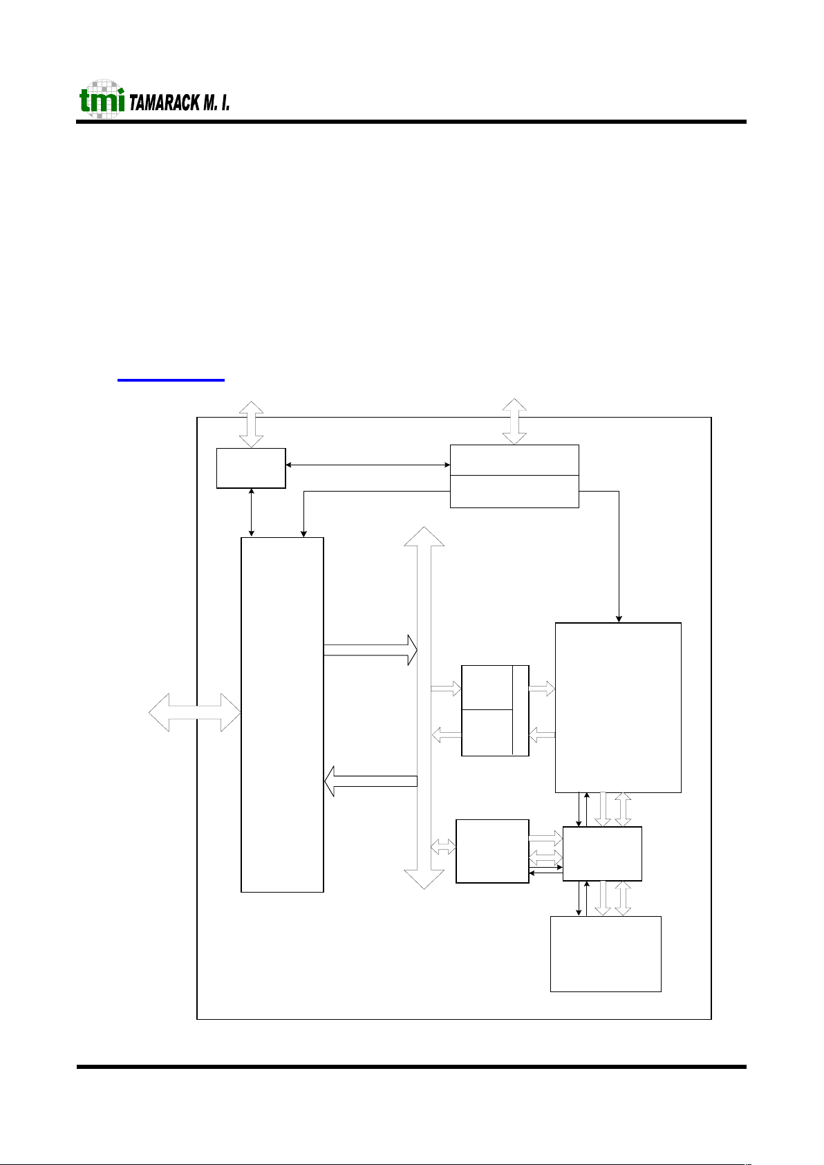
3 Block Diagram
From RX MAC
!
"
#
$$
#
#
$%&'(
)*
To TX MAC
%++*
%++*
,,
-
Page 5

TC6216M
- 5 -
Ver. 2.1
5/24/01
4 Pin Plcement
SDA
SCL
MIIMode
Vss_3.3V
RxClk
Vss_1.8V
RxDat153
RxDat152
RxDat151
RxDat150
Crs_Dv15
CRS15
Col15
Vdd_1.8V
TxClk
Vss_3.3V
TxDat153
TxDat152
TxDat151
TxDat150
TxEn15
Vdd_3.3V
RxDat141
RxDat140
Crs_Dv14
Vss_1.8V
TxDat141
TxDat140
TxEn14
Vdd_1.8V
RxDat131
RxDat130
Crs_Dv13
Vss_3.3V
TxDat131
TxDat130
TxEn13
Vdd_3.3V
RxDat121
RxDat120
Crs_Dv12
Vss_1.8V
TxDat121
TxDat120
TxEn12
Vdd_1.8V
RxDat111
RxDat110
Crs_Dv11
Vss_1.8V
TxDat111
TxDat110
208
207
206
205
204
203
202
201
200
199
198
197
196
195
194
193
192
191
190
189
188
187
186
185
184
183
182
181
180
179
178
177
176
175
174
173
172
171
170
169
168
167
166
165
164
163
162
161
160
159
158
157
Vss_3.3V 1 156 TxEn11
reset 2 155 Vdd_1.8V
TestMode 3 154 MDClk
Vdd_3.3V 4 153 MDIO
TnkA0 5 152 CLK75M
TnkA1 6 151 clk
Vdd_3.3V 7 150 Vdd_3.3V
TnkB0 8 149 refck
TnkB1 9 148 Vss_1.8V
Vss_1.8V 10 147 RxDat101
TnkMod0 11 146 RxDat100
Vss_3.3V 12 145 Crs_Dv10
TnkMod1 13 144 Vdd_1.8V
Vdd_1.8V 14 143 TxDat101
NC 15 142 TxDat100
PrtPri0 16 141 TxEn10
Vdd_3.3V 17 140 Vss_3.3V
PrtPri1 18 139 RxDat91
PrtPri2 19 138 RxDat90
Vss_1.8V 20 137 Crs_Dv9
PrtPri3 21 136 Vdd_3.3V
PrtPri4 22 135 TxDat91
Vss_3.3V 23 134 TxDat90
PrtPri5 24 133 TxEn9
PrtPri6 25 132 Vss_3.3V
Vdd_1.8V 26 131 RxDat81
PrtPri7 27 130 RxDat80
PriLev0 28 129 Crs_Dv8
Vdd_3.3V 29 128 Vdd_3.3V
PriLev1 30
127 TxDat81
PriLev2 31 126 TxDat80
Vss_1.8V 32 125 TxEn8
PriLev3 33 124 Vss_3.3V
PriLev4 34 123 RxDat71
Vdd_1.8V 35 122 RxDat70
PriLev5 36 121 Crs_Dv7
PriLev6 37 120 Vdd_1.8V
PriLev7 38 119 TxDat71
Vss_3.3V 39 118 TxDat70
Vdd_3.3V 40 117 TxEn7
EnIPPr 41 116 Vss_1.8V
EnVLPr 42 115 RxDat61
Vss_1.8V 43 114 RxDat60
FCBcstEn 44 113 Crs_Dv6
BcstAll 45 112 Vdd_1.8V
BcstTr 46 111 TxDat61
RejMCT 47 110 TxDat60
Vdd_1.8V 48 109 TxEn6
FcOpt 49 108 Vss_3.3V
Vdd_3.3V 50 107 RxDat51
DisBPBk 51 106 RxDat50
Vss_3.3V 52 105 Crs_Dv5
53
54
55
56
57
58
59
60
61
62
63
64
65
66
67
68
69
70
71
72
73
74
75
76
77
78
79
80
81
82
83
84
85
86
87
88
89
90
91
92
93
94
95
96
97
98
99
100
101
102
103
104
Vss_1.8V
DisBPr
FullBP
Vdd_1.8V
PowLED
OvBcLED
OVUnLED
Vss_3.3V
TxEn0
TxDat00
TxDat01
Vdd_3.3V
Crs_Dv0
RxDat00
RxDat01
Vss_3.3V
TxEn1
TxDat10
TxDat11
Vdd_1.8V
Crs_Dv1
RxDat10
RxDat11
Vss_1.8V
TxEn2
TxDat20
TxDat21
Vdd_1.8V
Crs_Dv2
RxDat20
RxDat21
Vss_1.8V
TxEn3
TxDat30
TxDat31
Vdd_1.8V
Crs_Dv3
RxDat30
RxDat31
Vss_1.8V
TxEn4
TxDat40
TxDat41
Vdd_3.3V
Crs_Dv4
RxDat40
RxDat41
Vss_3.3V
TxEn5
TxDat50
TxDat51
Vdd_3.3V
TC6216M
PQFP 208
Top View
Page 6

TC6216M
- 6 -
Ver. 2.1
5/24/01
5 Pin Listing (PQFP 208)
Pin Description Pin label Type Pin Description Pin label Type
1 Power Vss_3.3V ~ 105 RMII Crs_Dv5 I
2 Reset reset Ipu 106 RMII RxDat50 I
3 Configuration TestMode Ipd 107 RMII RxDat51 I
4 Power Vdd_3.3V ~ 108 Power Vss_3.3V ~
5 Configuration TnkA0 Ipd 109 RMII TxEn6 O
6 Configuration TnkA1 Ipd 110 RMII TxDat60 O
7 Power Vdd_3.3V ~ 111 RMII TxDat61 O
8 Configuration TnkB0 Ipd 112 Power Vdd_1.8V ~
9 Configuration TnkB1 Ipd 113 RMII Crs_Dv6 I
10 Power Vss_1.8V ~ 114 RMII RxDat60 I
11 Configuration TnkMod0 Ipd 115 RMII RxDat61 I
12 Power Vss_3.3V ~ 116 Power Vss_1.8V ~
13 Configuration TnkMod1 Ipd 117 RMII TxEn7 O
14 Power Vdd_1.8V ~ 118 RMII TxDat70 O
15 NC NC ~ 119 RMII TxDat71 O
16 Configuration PrtPri0 Ipd 120 Power Vdd_1.8V ~
17 Power Vdd_3.3V ~ 121 RMII Crs_Dv7 I
18 Configuration PrtPri1 Ipd 122 RMII RxDat70 I
19 Configuration Prtpri2 Ipd 123 RMII RxDat71 I
20 Power Vss_1.8V ~ 124 Power Vss_3.3V ~
21 Configuration PrtPri3 Ipd 125 RMII TxEn8 O
22 Configuration PrtPri4 Ipd 126 RMII TxDat80 O
23 Power Vss_3.3V ~ 127 RMII TxDat81 O
24 Configuration PrtPri5 Ipd 128 Power Vdd_3.3V ~
25 Configuration PrtPri6 Ipd 129 RMII Crs_Dv8 I
26 Power Vdd_1.8V ~ 130 RMII RxDat80 I
27 Configuration PrtPri7 Ipd 131 RMII RxDat81 I
28 Configuration PriLev0 Ipd 132 Power Vss_3.3V ~
29 Power Vdd_3.3V ~ 133 RMII TxEn9 O
30 Configuration PriLev1 Ipd 134 RMII TxDat90 O
31 Configuration PriLev2 Ipd 135 RMII TxDat91 O
32 Power Vss_1.8V ~ 136 Power Vdd_3.3V ~
33 Configuration PriLev3 Ipd 137 RMII Crs_Dv9 I
34 Configuration PriLev4 Ipd 138 RMII RxDat90 I
35 Power Vdd_1.8V ~ 139 RMII RxDat91 I
36 Configuration PriLev5 Ipd 140 Power Vss_3.3V ~
37 Configuration PriLev6 Ipd 141 RMII TxEn10 O
38 Configuration PriLev7 Ipd 142 RMII TxDat100 O
39 Power Vss_3.3V ~ 143 RMII TxDat101 O
40 Power Vdd_3.3V ~ 144 Power Vdd_1.8V ~
41 Configuration EnIPPr Ipd 145 RMII Crs_Dv10 I
Page 7

TC6216M
- 7 -
Ver. 2.1
5/24/01
Pin Description Pin label Type Pin Description Pin label Type
42 Configuration EnVLPr Ipd 146 RMII RxDat100 I
43 Power Vss_1.8V ~ 147 RMII RxDat101 I
44 Configuration FCBcstEn Ipu 148 Power Vss_1.8V ~
45 Configuration BcstAll Ipu 149 CLK refck I
46 Configuration BcstTr Ipd 150 Power Vdd_3.3V ~
47 Configuration RejMCT Ipu 151 CLK clk I
48 Power Vdd_1.8V ~ 152 CLK CLK75M O
49 Configuration FcOpt Ipu 153 MDIO MDIO I/Opu
50 Power Vdd_3.3V ~ 154 MDIO MDClk O
51 Configuration DisBPBk Ipd 155 Power Vdd_1.8V ~
52 Power Vss_3.3V ~ 156 RMII TxEn11 O
53 Power Vss_1.8V ~ 157 RMII TxDat110 O
54 Configuration DisBPr Ipd 158 RMII TxDat111 O
55 Configuration FullBP Ipd 159 Power Vss_1.8V ~
56 Power Vdd_1.8V ~ 160 RMII Crs_Dv11 I
57 LED PowLED OL 161 RMII RxDat110 I
58 LED OvBcLED OL 162 RMII RxDat111 I
59 LED OvUnLED OL 163 Power Vdd_1.8V ~
60 Power Vss_3.3V ~ 164 RMII TxEn12 O
61 RMII TxEn0 O 165 RMII TxDat120 O
62 RMII TxDat00 O 166 RMII TxDat121 O
63 RMII TxDat01 O 167 Power Vss_1.8V ~
64 Power Vdd_3.3V ~ 168 RMII Crs_Dv12 I
65 RMII Crs_Dv0 I 169 RMII RxDat120 I
66 RMII RxDat00 I 170 RMII RxDat121 I
67 RMII RxDat01 I 171 Power Vdd_3.3V ~
68 Power Vss_3.3V ~ 172 RMII TxEn13 O
69 RMII TxEn1 O 173 RMII TxDat130 O
70 RMII TxDat10 O 174 RMII TxDat131 O
71 RMII TxDat11 O 175 Power Vss_3.3V ~
72 Power Vdd_1.8V ~ 176 RMII Crs_Dv13 I
73 RMII Crs_Dv1 I 177 RMII RxDat130 I
74 RMII RxDat10 I 178 RMII RxDat131 I
75 RMII RxDat11 I 179 Power Vdd_1.8V ~
76 Power Vss_1.8V ~ 180 RMII TxEn14 O
77 RMII TxEn2 O 181 RMII TxDat140 O
78 RMII TxDat20 O 182 RMII TxDat141 O
79 RMII TxDat21 O 183 Power Vss_1.8V ~
80 Power Vdd_1.8V ~ 184 RMII Crs_Dv14 I
81 RMII Crs_Dv2 I 185 RMII RxDat140 I
82 RMII RxDat20 I 186 RMII RxDat141 I
83 RMII RxDat21 I 187 Power Vdd_3.3V ~
84 Power Vss_1.8V ~ 188 (R)MII TxEn15 O
Page 8

TC6216M
- 8 -
Ver. 2.1
5/24/01
Pin Description Pin label Type Pin Description Pin label Type
85 RMII TxEn3 O 189 (R)MII TxDat150 O
86 RMII TxDat30 O 190 (R)MII TxDat151 O
87 RMII TxDat31 O 191 (R)MII TxDat152 O
88 Power Vdd_1.8V ~ 192 (R)MII TxDat153 O
89 RMII Crs_Dv3 I 193 Power Vss_3.3V ~
90 RMII RxDat30 I 194 CLK TxClk I
91 RMII RxDat31 I 195 Power Vdd_1.8V ~
92 Power Vss_1.8V ~ 196 (R)MII Col15 I
93 RMII TxEn4 O 197 (R)MII Crs15 I
94 RMII TxDat40 O 198 (R)MII Crs_Dv15 I
95 RMII TxDat41 O 199 (R)MII RxDat150 I
96 Power Vdd_3.3V ~ 200 (R)MII RxDat151 I
97 RMII Crs_Dv4 I 201 (R)MII RxDat152 I
98 RMII RxDat40 I 202 (R)MII RxDat153 I
99 RMII RxDat41 I 203 Power Vss_1.8V ~
100 Power Vss_3.3V ~ 204 CLK RxClk I
101 RMII TxEn5 O 205 Power Vss_3.3V ~
102 RMII TxDat50 O 206 Configuration MIIMode Ipd
103 RMII TxDat51 O 207 EEPROM SCL O
104 Power Vdd_3.3V ~ 208 EEPROM SDA I/Opu
I ⇒ digital input
I
pd
⇒ digital input internally pulled down
I
pu
⇒ digital input internally pulled up
O ⇒ digital output
O
L
⇒ digital output active low
I/O
pu
⇒ digital bidirectional internally pulled up
6 Pin Description
Interface Signal I/O Signal Description
reset I General reset.
Clk I System clock. The switch performance is full wire speed at
50Mhz system clock freq uency.
Control/Clock
Clk75M O Output clock from internal PLL. For 75MHz system clock
frequenc y tie this to system clock pin.
Test TestMode I
If set to ′1′ the chip will be in Memory Test Mode.
Trunking TnkA(0:1)
TnkB(0:1)
I Trunking configuration.
•
First trunk channel
TnkA1 TnkA0
0 0 No port is configured as trunk port
0 1 Ports 0 and 1 are configured as trunk ports
1 0 Ports 0,1,2 are configured as trunk ports
1 1 Ports 0,1,2 and 3 are configured as trunk ports
•
Second trunk channel
TnkB1 TnkB0
0 0 No port is configured as trunk port
0 1 Ports 15 and 14 are configured as trunk ports
1 0 Ports 15, 14 , 13 are configu r ed as trunk ports
Page 9

TC6216M
- 9 -
Ver. 2.1
5/24/01
Interface Signal I/O Signal Description
1 1 Ports 15, 14 , 13 and 12 are configured as trunk
ports
TnkMod(0:1) I Trunk Balance Mode Select
TnkMod1 TnkMod0
0 0 Only source port is used to select the transmission port
inside the trunk.
0 1 Transmission port is selected using SA.
1 0 Transmission port is selected using SA and DA.
1 1 Not used
PrtPri (0:7) I Indicates which ports, if any, are in Priority Mode; when
selected the corresponding port will have high or very high
priority depending of the state of PriLev pin.
PrtPri(0:7) are used to set the priorities for por ts 4 to 11.
TC6216M Port (4 to 11) ! PrtPri (0:7)
PriLev (0:7) I Selects the high or very high priority for priority ports.
′1′ – Very high priority
′0′ – High priority
PriLev (0:7) refers to TC6216M ports 4 to 11.
EnIPPr I Enables QoS resolution to consider TOS Precedence bits from
IP Header.
′1′ – IP priority will be considered
′0′ – IP priority will be neglected
QoS configuration
EnVLPr I Enables QoS resolution to consider user_prio r ity bits (TCI
field) from 802.1Q VLAN Tag Header.
′1′ – VLAN priority will be considered
′0′ – VLAN priority will be neglected
FcBcstEn I Enables Flow Control for Broadcast operation.
′1′ – Enable
′0′ – Disable
BcstAll I Br oadcast All Mode Select
′1′– forward broadcast packes to all the ports
′0′– forward broadcast packes to active ports only
Broadcast
configuration
BcstTr I Enables br oadcast throttling.
′1′– Enable
′0′– Disable
MII Mode
Selection
MIIMode I Select MII or RMII interface for port 15
′0′– RMII
′1′– MII
MAC
Configuration
RejMCT I All Mac Control Type Packets will be rejected if this pin is
asserted, otherwise they will be forwarded.
FCOpt I Flow Control resolution option:
′1′- the A-NEG result is considered
′0′– doesn't matter the A-NEG result
DisBPr I Enable / Disable Flow Control for Half Duplex Mode
′1′– Disable
′0′– Enable
Flow Control
FullBP I
When this is set to ′0′ then the backpressure process will be
stopped after reaching 30 consecutive collisions. The default
value (30) can be changed by EEPROM settings. Otherwise the
backpressure can be executed for up to 2048 (default pause
value) slot times if the flow control condition persists.
Page 10

TC6216M
- 10 -
Ver. 2.1
5/24/01
Interface Signal I/O Signal Description
DisBPBk I Disables completely any backoff when executing backpressure:
′1′– no backoff when backpressure
′0′– aggressive backoff for backpressure
Power and BIST PowLED O Signals good operation state. In case of BIST error the code of
the error is signaled on this pin.
OvBcLED O Signals overflow condition for broadcast operation. Overflow signaling
OvUnLED O Signals overflow condition for unicast op e r a tion.
SDA I/O Serial Data. EEPROM
Interface
SCL O Serial Clock.
MDIO I/O MDIO BUS. MDIO Interface
MDClk O MDIO clock.
TxDat0(0:1) O RMII Tx Data.
TxEn0 O RMII Tx Enable.
Crs_Dv0 I RMII Carrier Sense / Receive Data Valid.
RMII Interface
Port0
RxDat0(0:1) I RMII Rx Data.
TxDat1(0:1) O RMII Tx Data
TxEn1 O RMII Tx Enable.
Crs_Dv1 I RMII Carrier Sense / Receive Data Valid
RMII Interface
Port1
RxDat1(0:1) I RMII Rx Data.
TxDat2(0:1) O RMII Tx Data
TxEn2 O RMII Tx Enable
Crs_Dv2 I RMII Carrier Sense / Receive Data Valid
RMII Interface
Port2
RxDat2(0:1) I RMII Rx Data
TxDat3(0:1) O RMII Tx Data
TxEn3 O RMII Tx Enable
Crs_Dv3 I RMII Carrier Sense / Receive Data Valid
RMII Interface
Port3
RxDat3(0:1) I RMII Rx Data
TxDat4(0:1) O RMII Tx Data
TxEn4 O RMII Tx Enable
Crs_Dv4 I RMII Carrier Sense / Receive Data Valid
RMII Interface
Port4
RxDat4(0:1) I RMII Rx Data
TxDat5(0:1) O RMII Tx Data
TxEn5 O RMII Tx Enable
Crs_Dv5 I RMII Carrier Sense / Receive Data Valid
RMII Interface
Port5
RxDat5(0:1) I RMII Rx Data
TxDat6(0:1) O RMII Tx Data
TxEn6 O RMII Tx Enable
Crs_Dv6 I RMII Carrier Sense / Receive Data Valid
RMII Interface
Port6
RxDat6(0:1) I RMII Rx Data
TxDat7(0:1) O RMII Tx Data
TxEn7 O RMII Tx Enable
Crs_Dv7 I RMII Carrier Sense / Receive Data Valid
RMII Interface
Port7
RxDat7(0:1) I RMII Rx Data
Page 11

TC6216M
- 11 -
Ver. 2.1
5/24/01
Interface Signal I/O Signal Description
TxDat8(0:1) O RMII Tx Data
TxEn8 O RMII Tx Enable
Crs_Dv8 I RMII Carrier Sense / Receive Data Valid
RMII Interface
Port8
RxDat8(0:1) I RMII Rx Data
TxDat9(0:1) O RMII Tx Data
TxEn9 O RMII Tx Enable
Crs_Dv9 I RMII Carrier Sense / Receive Data Valid
RMII Interface
Port9
RxDat9(0:1) I RMII Rx Data
TxDat10(0:1) O RMII Tx Data
TxEn10 O RMII Tx Enable
Crs_Dv10 I RMII Carrier Sense / Receive Data Valid
RMII Interface
Port10
RxDat10(0:1) I RMII Rx Data
TxDat11(0:1) O RMII Tx Data
TxEn11 O RMII Tx Enable
Crs_Dv11 I RMII Carrier Sense / Receive Data Valid
RMII Interface
Port11
RxDat11(0:1) I RMII Rx Data
TxDat12(0:1) O RMII Tx Data
TxEn12 O RMII Tx Enable
Crs_Dv12 I RMII Carrier Sense / Receive Data Valid
RMII Interface
Port12
RxDat12(0:1) I RMII Rx Data
TxDat13(0:1) O RMII Tx Data
TxEn13 O RMII Tx Enable
Crs_Dv13 I RMII Carrier Sense / Receive Data Valid
RMII Interface
Port13
RxDat13(0:1) I RMII Rx Data
TxDat14(0:1) O RMII Tx Data
TxEn14 O RMII Tx Enable
Crs_Dv14 I RMII Carrier Sense / Receive Data Valid
RMII Interface
Port14
RxDat14(0:1) I RMII Rx Data
TxDat15(0:3) O RMII Tx Data (0:1) / MII Tx Data (0:3)
RxDat15(0:3) I RMII Rx Data (0:1) / MII Rx Data (0:3)
TxEn15 O RMII / MII Tx Enable
Crs_Dv15 I RMII Carrier Sense / Receive Data Valid
Col15 I MII Collision.
TxClk15 I MII Tx Clock.
RxClk15 I MII Rx Clock.
(R)MII Interface
Port15
CRS15 I MII Carrier Sense.
RMII
Reference Clock
refck I RMII Reference Clock for Port 0-15
Page 12

TC6216M
- 12 -
Ver. 2.1
5/24/01
7 Ethernet Media Access Controller
The Ethernet Media Access Controller (MAC) contains IEEE 802.3 MAC functions for 16 ports. It is able to
operate in 10/100 speed modes, full and half duplex. Each port has its dedicated receive and transmit FIFO′s
with necessary logic to implement flow-control for both duplex modes. The MAC functions are optimized and
tailored for high speed and flexible interfacing.
7.1 Receive MAC
When a frame is received from the Ethernet media through the RMII, the data is stored in a receive FIFO. The
FIFO acts as a temporary buffer between the Receive MAC section and switch core interface.
The Receive MAC layer decomposes Ethernet packets acquired from the PHY layer via RMII, by stripping off
the preamble sequence and SFD. The Receive MAC then sends packets to the receive FIFO along with packet
validity information.
The MAC determines the validity of each received packet by checking the CRC and packet length. The bad
packets will be dropped either by the MAC or by the queue manager. Oversized packets are truncated to 1536
bytes and marked to be erroneous. Undersized packets are removed from the receive FIFO without being
reported at the switch interface. The FIFO space held by undersized packets is automatically recovered by
removing the packet.
The Receive MAC is also able to reject Mac Control Type frames (type 88-08). To activate this filtering function
it must be selected using RejMCT pin or the equivalent EEP ROM bit.
When the TC6216M receives a MAC control frame and determines that the opcode is a PAUSE command (flow
control frame) and the frame
′
s CRC is OK, the chip will load its internal pause counter with the ′time val ue′
variable extracted from the incoming flow control packet. If the pause counter is not
′
zero′ the Receive MAC will
XOFF the Transmit MAC. The pause counter will decrement after each slot time and will XON the Transmit
MAC when the
′
zero′ value is reached.
If a frame transmission is in progress when the PAUSE frame is received, the transmission is allowed to
complete but it will be stopped for the next packets until an XON command is generated by the Receive MAC.
The pause time will begin at the end of current transmission or immediately (if no transmission is in course at the
moment of receiving the PAUSE frame). If a pause command is received while the transmitter is already in
pause, the new pause time indicated by the new Flow Control frame will be loaded into the pause register.
When the receive FIFO is full and additional data are still incoming from the MAC, then the overrun condition
occurs and the frame is dropped. If the system clock frequency is not lower than the recommended value this
condition will not occur.
7.2 Transmit MAC
The Transmit MAC section assembles the MAC frames stored in the transmit FIFO and controls their
transmission onto the media via external PHY entities. It appends the standard preamble and start of frame
delimiter to the transmitted packets. The Transmit MAC also controls the InterFrameGap time during
transmission, maintaining for default the standard minimu m InterFrameGap of 96 bit time. This value can be
changed by EEPROM setting.
For half duplex mode the Transmit MAC meets CSMA/CD IEEE 802.3 requirements. The FIFO logic manages
frame retransmission for early collision conditio ns or discards the frame if late collision occurs. It also follows
the truncated binary exponential backoff algorithm, collision and jamming procedures.
The transmit FIFO buffers the packets available for transmission in the main memory queues. If the transmit
FIFO gets empty before the packet currently in transmissio n reaches its end, an underrun conditio n is generated.
When the switch core transfers the rest of the packet into the FIFO the Transmit MAC safely discards it without
affecting the next packet. Underrun conditions will not occur if the system is operated at the reco mmended clock
frequency or higher.
For full duplex mode the TC6216M implements the flow-control algorithm according with the IEEE 802.3x
standard. T he chip uses the XON/XOFF method adjusting the Pause Value field inside the MAC Pause Frame
according to traffic conditions. The full duplex flow control can be enabled/disabled depending on
autonegotiation result, pin configuration and/or EEPROM settings.
The TC6216M executes backpressure algorithm as half duplex flow control mode if not disabled by DisBPr pin
or EEPROM (ConfigRegPx[1]). The backpressure algorithm is based on carrier sense forced collisions and a n
aggressive backoff algorithm. The forced consecutive collisions generated for flow control purposes can be
Page 13

TC6216M
- 13 -
Ver. 2.1
5/24/01
limited to a maximum of 30 collisions if this option is selected. The default number of consecutive co llisio ns can
be changed by EEPROM settings. This feature can be used to avoid HUB partitioning.
MAC Block Diagram
8 Traffic Priority
TC6216M supports advanced traffic priority features (QoS). It provides three levels of priority: normal, high
and very high priority. Each class of priority has its dedicated queue for each transmission port. Packets in
priority mode (high or very high priority) will arrive sooner at the destination MAC address. When all (3)
priority queues for the same port are not empty the transmission bandwidth is used around 8% for the low
priority queue, 30% for high priority and 62% for very high priority queue. The bandwidth distribution when one
of the queues is empty can be observed in the table below:
Transmission Bandwidt h Utilization Factor Priority Queues
IF Empty
Normal (Low)
Priority
High Priority
Very High
Priority
Normal X 33% 66%
High 11% X 89%
Very High 20% 80% X
None 8% 30% 62%
These priority rules apply for all ports and are independent of the port′s speed mode or duplex mode.
A special packet dropping mechanism is also implemented to offer more protection against overflow conditions
for priority packets. If the packet memory load is exceeding an overflow threshold then all normal priority
packets will be dropped on source port basis in order to save space for the priority packets. This will minimize
the probability of packet loss in priority flows for senders that are not flo w-contro l cap able.
Rx FIFO
Rx MAC Tx MAC
Flow
Control
Tx FIFO
Fifo Contro l Logic
System Interface
MAC
RMII
PHY Layer
RM II Rx D a ta (2)
Tx D a ta (64)FC I nse rtTi me Value (16)Rx Dat a (64)
RM II Tx D a ta (2 )
FIFO
Control
Logic
Page 14

TC6216M
- 14 -
Ver. 2.1
5/24/01
The QoS mechanism supports multiple prioritization sources. Packet priority can be checked via 802.1Q VLAN
Tag Header TCI bits (layer 2) and/or IP Header TOS bits (layer 3). If the value of TCI/TOS bits is “0”, this
packet will be treated as normal priority, if “1” then it will be high priority, if more than “1” then it will be very
high priority. Port based prioritization is also available. Using port based priority the user can assign different
priorities for each port. If VLAN and IP priority are disabled or not labeled, all packets received on the same por t
will be forwarded with the corresponding assigned port base priority. When more than one prioritization
methods are active at the same time (VLAN, IP and/or port based) the priority resolution consists of maximizing
the priority class.
The QoS can be configured using both pin configuration interface and/or EEPROM settings. The VLAN
prioritization can be enabled by EnVLPr pin or by PriorityReg[0] EEPROM bit, while EnIPPr pin or
PriorityReg[1] EEPROM bit can be used to enable the IP priority. Port based prioritization is available using
PrtPri(x) and PriLev(x) pins for port 4 to 11, or equivalent EEPROM bits ConfigRegPx[3] and
ConfigRegPx[2] for each ports. Setting PrtPri(x) pin to
′1′
will configure the corresponding port in Pr iority
Mode. PriLev(x) pin selects between high (
′0′
) and very high priority (′1′).
9 Trunk Configuration
TC6216M can setup two port aggregation links, named ′Trunk A′ respectively ′Trunk B ′, of up to 4 ports each.
Using this feature multiple TC6216M can be cascaded or interconnected with other switches supporting the
trunking feat ur e .
The trunks can be independently configured according with tables below using pin configuration
TnkA0
,
TnkA1
respectively
TnkB0 ,TnkB1
or using EEPROM configur ation (TrunkCfgReg).
TnkA1 TnkA0 Ports grouped within Trunk A
′0 ′ ′0 ′
Trunk A disabled
′0 ′ ′1 ′
Trunk A groups ports 0 and 1
′1 ′ ′0 ′
Trunk A groups ports 0,1 and 2
′1 ′ ′1 ′
Trunk A groups ports 0,1 ,2 and 3
TnkB1 TnkB0 Ports grouped within Trunk B
′0 ′ ′0 ′
Trunk B disabled
′0 ′ ′1 ′
Trunk B gro ups ports 14 and 15
′1 ′ ′0 ′
Trunk B gro ups ports 13,14 and 15
′1 ′ ′1 ′
Trunk B gro ups ports 12,13,14 and 15
The traffic on the ports of the same trunk will be automatically balanced. TC6216M can be selected from three
balancing methods based on source port, SA and DA as shown in the table below. They are selectable from
TnkMod(0-1) pins or from EEPROM Tr unkCfgReg register:
TnkMod1 TnkMod0 Method Description
′0 ′ ′0 ′
Method 1. based on source port.
′0 ′ ′1 ′
Method 2. based on SA.
′1 ′ ′0 ′
Method 3. based on SA and DA.
′1 ′ ′1 ′
Not used
Different stations connected on the same port may not send traffic on the same trunk line. The packet order is
guaranteed for method 1 and 2 for unicast and broadcast packets. The packet order is guaranteed for method 3
only for unicast packets.
The default mode for all trunking ports is 100Mbps full duplex. Trunk port modes can be changed using
EEPROM settings although this is not recommended. Also it is recommended for trunk ports to be
interconnected with 100Mbps full duplex capable ports only. If the user selects a trunk configuration it must
Page 15

TC6216M
- 15 -
Ver. 2.1
5/24/01
make sure that all ports are connected within the trunk, the port order is not mandatory. If one wire from a
defined trunk is not connected, the trunk may not work properly.
10 Flow Control
TC6216M executes backpressure for half duplex and is IEEE 802.3x compliant for full duplex flow control
operation. The chip uses XON/XOFF flow control method in full duplex mode.
For full duplex operation, if no EEPROM is used and FCOpt pin is asserted the autonegotiation flow control
capability resolution is execute d. This means that if bit 10 from the Link Partner Advertise ment Register is not
set then the transmission of flo w control packets is d isabled. If FCOpt is ′0′ then the entire flow control operation
for full duplex is always executed. The flow control on the receive side is always operational disregarding the
state of FCOpt pin. FCOpt pin represents a global setting for all 16 ports.
When the EEPROM is used, the FCOpt can be override by its equivalent bit FlowControlReg[0]. Supplementary
a setting is offered per port b asis DsFulDpxFC (ConfigRegPx[4]). Setting this bit to ′1′ will disable the flow
control on that port no matter of autonegotiation result.
Without EEPROM
FCOpt
Pin
A-NEG
(bit 10 from the PHY's Link
Partner Register)
FC – Ability
0
Don′t care
Enabled
Disabled Disabled 1
Enabled Enabled
With EEPROM
FCOpt
Bit
(FlowControlReg)
DsFulDpxFc
Bit
(ConfigRegP x )
A-NEG
(bit 10 from the PHY's Link
Partner Register)
FC – Ability/Port
1 Disabled 0
0
Don′t care
Enabled
1
Don′t care
Disabled
Disabled Disabled
1
0
Enabled Enabled
The backpressure operation can also be disabled using DisBPr pin or per port base using EEPROM
(ConfigRegPx[1]). In case a HUB with many workstations is connected to a port, the HUB may be partitio ned in
heavy traffic when the switch executes too musch continuous backpressure. TC6216M can prevent this when
FullBP pin is not asserted by discontinuing the backpressure process after a determined number of consecutive
collisions is reached. This number can be specified using FlowControlReg, field B ackP r Lv.
11 Broadcast
In case of excessive broadcast the traffic can be throttled on source port basis. TC6216M implements an evolved
throttling method based on both por t bandwidth and bro adcast memory utilizatio n. This feature is e nabled using
BcstTr configuration pin or the EEPROM BroadcastReg[2] bit.
The memory used at any time by broadcast packets that are received from the same port can not exceed a preset
amount. This is represented by a number of 256 byte packet buffers that can be set using BroadcastReg
EEPROM register, field MemThrotReg. When no EEPROM is present the default value of 8 buffers is used.
When more than this number of buffers are in use by broadcast packets, any other broadcast incoming from the
respective port will be dropped.
Page 16

TC6216M
- 16 -
Ver. 2.1
5/24/01
The broadcast receive bandwidth per port can be reduced to a value between 1.5% to 22% of the port′s
maximum bandwidth. When the broadcast bandwidth exceeds the preset value so me broadcast packets will be
dropped. The throttling bandwidth can be adjusted using register BroadcastReg, field BndwThrotReg. It is
obtained by multiplying the value in this field with 1.5%. The default value is 4 (6%) .
Supplementary, but not depending of the broadcast throttling configuration, all broadcast packets will be
dropped when the total amount of the memory used by broadcast packets exceeds a preset threshold. This
situation will occur only whe n flow contr ol for bro adcast is disab led, otherwise no broad cast packet will b e lost.
The flow control for broadcast traffic can be enabled using FcBcstEn pin or EEPROM (BroadcastReg[1]). Even
when broadcast flow control is disabled TC6216M is capable of taking continuos broadcast packets from one
port and deliver them to all the other ports at maximum speed without losing packets.
When TC6216M is configured in BroadcastAll mode all broadcast packets will be sent to all ports. If
BroadcastAll mode is disabled the broadcast packets will be sent only to ports that have the link status on. Link
status is monitored by the PHY polling entity t hat also r eads the port mode autonegotiation result.
12 Auto Negotiation
In Auto-Negotiation Mode (assumed by default when the EEPROM is not present) TC6216M is polling the
PHY′s RMII Management Registers using the MDIO line in order to extract the autonegotiated port mode
information, full duplex flow control abilit y and the link status. The switch detects and follo ws any changes in
less than 2 seconds.
After reset TC6216M advertises the full duplex flow control capability (writing ′1′ to bit 10 from PHY′s
Advertisement Register) and restarts the autonegotiation.
If the port mode (speed and duplex) is forced by EEPROM settings then this mode is also advertised before
restarting the autonegotiation. In this case TC6216M will not advertise any other speed or duplex capability
other than what is set by EEPROM. Port mode can be forced using ConfigRegPx bits 5 – 7.
13 EEPROM Interface
TC6216M can be configured using a serial EEPROM device type AT24C02A (2048 bits organized as 256 pages
of 1 byte each). With this device the manufacturer can deliver a pre-configured system to their customers while
the customers can reconfigure the system and retain their preferences.
The TC6216M is able to operate without EEPROM and can make effective use of its features using only the pin
configuration interface. The EEPROM configuration provides additional features and it can override all pin
interface settings offering a jumperless configuration mode. For this reason, equivalent EEPROM settings can be
found for every configuration pin.
A validation bit is provided for each one of the EEPROM Configuration Registers. A dedicated Validation
Register is reserved for this purpose and corresponding bits from this register must be set in order to enable the
desired EEPROM configurat ions.
The EEPROM configuration information is accessed by the TC6216M after each reset procedure.
14 Programming the EEPROM for configuration
If the ′Reset′ pin is hold low, the TC6216M′s EEPROM interface will go into high impedance state. This feature
enables easy programming of the EEPROM during installation or configuration.
The EEPROM can be programmed using an external parallel port. A dedicated signal from this port can be used
to hold the RESET pin low. Once the TC6216M interface pins have got to the high impedance state the
EEPROM can be programmed by the parallel port through the SDA and SCL pins.
To enable the AT24C02A device to be accessed by the TC6216M, its page address input pins must be hardwired
to ′0′.
Page 17

TC6216M
- 17 -
Ver. 2.1
5/24/01
15 EEPROM Address Map
EEPROM
Physical
Address
Bits
Register Name Validation
Bit
DESCRIPTION
00 [7:0] ValidReg [ 23 downto 16 ] - Validate Registers
01 [7:0] ValidReg [ 15 downto 8 ] - Validate Registers
02 [7:0] ValidReg [ 7 downto 0 ] - Validate Registers
03 [7:0] ConfigRegP0 [ 7 downto 0 ] ValidReg [ 0 ] Port 0 Configuration Register
04 [7:0] ConfigRegP1 [ 7 downto 0 ] ValidReg [ 1 ] Port 1 Configuration Register
05 [7:0] ConfigRegP2 [ 7 downto 0 ] ValidReg [ 2 ] Port 2 Configuration Register
06 [7:0] ConfigRegP3 [ 7 downto 0 ] ValidReg [ 3 ] Port 3 Configuration Register
07 [7:0] ConfigRegP4 [ 7 downto 0 ] ValidReg [ 4 ] Port 4 Configuration Register
08 [7:0] ConfigRegP5 [ 7 downto 0 ] ValidReg [ 5 ] Port 5 Configuration Register
09 [7:0] ConfigRegP6 [ 7 downto 0 ] ValidReg [ 6 ] Port 6 Configuration Register
0A [7:0] ConfigRegP7 [ 7 downto 0 ] ValidReg [ 7 ] Port 7 Configuration Register
0B [7:0] ConfigRegP8 [ 7 downto 0 ] ValidReg [ 8 ] Port 8 Configuration Register
0C [7:0] ConfigRegP9 [ 7 downto 0 ] ValidReg [ 9 ] Port 9 Configuration Register
0D [7:0] ConfigRegP10 [ 7 downto 0 ] ValidReg [ 10 ] Port 10 Configuration Register
0E [7:0] ConfigRegP11 [ 7 downto 0 ] ValidReg [ 11 ] Port 11 Configuration Register
0F [7:0] ConfigRegP12 [ 7 downto 0 ] ValidReg [ 12 ] Port 12 Configuration Register
10 [7:0] ConfigRegP13 [ 7 downto 0 ] ValidReg [ 13 ] Port 13 Configuration Register
11 [7:0] ConfigRegP14 [ 7 downto 0 ] ValidReg [ 14 ] Port 14 Configuration Register
12 [7:0] ConfigRegP15 [ 7 downto 0 ] ValidReg [ 15 ] Port 15 Configuration Register
13 [7:0] FCPauseVal [ 15 downto 8 ] ValidReg [ 16 ] Flow Control Pause Value
14 [7:0] FCPauseVal [ 7 downto 0 ] ValidReg [ 16 ] Flow Control Pause Value
15 [7:0] MACCfgReg [ 7 downto 0 ] ValidReg [ 17 ] MAC Configuration Register
16 [7:0] FlowControlReg [9 downto 8] ValidReg [ 18 ] Flow Control Register High
17 [7:0] FlowControlReg [7 downto 0] ValidReg [ 18 ] Flow Control Register Low
18 [7:0] TrunkCfgReg [ 7 downto 0 ] ValidReg [ 19 ] Trunk Configuration Register
19 [7:0] BroadcastReg [ 11 downto 8 ] ValidReg [ 20 ] Broadcast Configuration Register
High
1A [7:0] BroadcastReg [ 7 downto 0 ] ValidReg [ 20 ] Broadcast Configuration Register
Page 18

TC6216M
- 18 -
Ver. 2.1
5/24/01
EEPROM
Physical
Address
Bits
Register Name Validation
Bit
DESCRIPTION
Low
1B [7:0] PriorityReg [ 15 downto 8 ] ValidReg [ 21 ] Reserved
1C [7:0] PriorityReg [ 7 downto 0 ] ValidReg [ 21 ] Priority Register Low
16 Register Description
Validation Register
- Address: 00h-02h
23 0
ValidReg
Bit(s)
Field Dscription
23 –22 Not Used
21 – 0 ValidReg EEPROM Configuration Validation Register
ValidReg – each bit from this field corresponds to an EEPROM Configuration Register. Configurations made
using any of the EEPROM registers will be in force only if the register is valida ted by setting to ′1′
the corresponding bit in this register.
ValidReg [ 0 ] – validation bit for ConfigRegP0 register
ValidReg [ 1 ] – validation bit for ConfigRegP1 register
ValidReg [ 2 ] – validation bit for ConfigRegP2 register
ValidReg [ 3 ] – validation bit for ConfigRegP3 register
ValidReg [ 4 ] – validation bit for ConfigRegP4 register
ValidReg [ 5 ] – validation bit for ConfigRegP5 register
ValidReg [ 6 ] – validation bit for ConfigRegP6 register
ValidReg [ 7 ] – validation bit for ConfigRegP7 register
ValidReg [ 8 ] – validation bit for ConfigRegP8 register
ValidReg [ 9 ] – validation bit for ConfigRegP9 register
ValidReg [ 10 ] – validation bit for ConfigRegP10 register
ValidReg [ 11 ] – validation bit for ConfigRegP11 register
ValidReg [ 12 ] – validation bit for ConfigRegP12 register
ValidReg [ 13] – validation bit for ConfigRegP13 register
ValidReg [ 14 ] – validation bit for ConfigRegP14 register
ValidReg [ 15 ] – validation bit for ConfigRegP15 register
ValidReg [ 16 ] – validation bit for FCPauseVal register
ValidReg [ 17 ] – validation bit for MACCfgReg register
ValidReg [ 18 ] – validation bit for FlowControlReg register
ValidReg [ 19 ] – validation bit for TrunkCfgReg register
ValidReg [ 20 ] – validation bit for BroadcastReg register
ValidReg [ 21 ] – validation bit for PriorityReg register
Port x Configuration Register
- Address: 03h-12h
- Note: x = 0 to 15
Page 19

TC6216M
- 19 -
Ver. 2.1
5/24/01
01234567
Mode
Duplex
S
pee
d
PrtPr
i
DsFulDpxFC
PriLev
DisBackPr
Not Use
d
Bit(s)
Field Description
7 Mode Select source
6 Duplex Full / Half Duplex Configuration
5 Speed 100 Mbps / 10Mbps Configuration
4 DsFulDpxFC Disable Full Duplex Flow Control
3 PrtPri Port Priority
2 PriLev Priority Level
1 EnBackPr Enable Backpressure
0 Not Used
Mode – This bit selects the source of port mode configuration:
Mode Duplex Speed
0 Auto – Negotiation Auto – Negotiation
1 EEPROM configuration EEPROM configuration
Duplex
– if ′Mode′ configuration is ′1′ this bit will set the port′s duplex mode. When high
the port will be set in Full Duplex, when low it is Half Duplex.
Speed
– if ′Mode′ configuration is ′1′ this bit will set the port′s speed mode. When
high the port′s data rate is 100Mbps, when low it is 10Mbps.
DsFulDpxFC
– Setting this bit to 1 will disable trans mit Full Duplex Flow Control for port X.
- Default ′0′
PortPriority
– When set forces port X in Priority Mode, otherwise the port will have normal
priority.
PriorityLevel
– If the corresponding port is in Priority Mode then the port will have a very
high priority rate if this bit is asserted, otherwise only high pr iority rate.
Flow Control Pause Value
- Address: 14h-13h
15 14 10111213 0123456789
FCPauseVal
Bit(s)
Field Description
15 – 0 FCPauseVal Flow Control Pause Value
Page 20

TC6216M
- 20 -
Ver. 2.1
5/24/01
FCPauseVal
– 16-bits of data used by every port to determine backpressure duration after a flow
control XOFF condition occurs. This value does not need to be adjusted b y user.
- default ′0000100000000000′= 2048
MAC Configuration Register
- Address: 15h
01234567
Bit(s)
Field Description
7 FwdBCRC Forward Bad CRC Packets
6 RejMACType Reject MAC Control Type Frames
5 PHYAddr16 MDIO PHY Address 16 to 31
4 – 0 IFGConfig Interframe Gap Configuration
FwdBCRC
– When set to ′1′ the switch will not filter bad CRC frames with valid sizes. T his
kind of frames will be forwarded as they were received (without correcting the
CRC).
- Default ′0′
PHYAddr16
– Setting this bit to ′1′ will program the PHY polling entit y to use device address
range 16 to 31 instead of range 0 to 15.
- Default ′0′
RejMACType
– When asserted the switch filters all MAC Control Type frames (type 8808).
IFGConfig
– These bits are used to set the minimum IFG. If default value is set then the IFG
will have the standard minimum value of 960 ns, otherwise for one unit added the
minimum IFG will be increased with 40 ns.
- Default ′10101′ = 21
Flow Control Register
- Address: 17h-16h
15 14 10111213 0123456789
FlowControlReg
Not Used
BackPrLv
FullBP
DisBPBk
FcOpt
FairBackOff
Bit(s)
Field Description
Page 21

TC6216M
- 21 -
Ver. 2.1
5/24/01
15 – 10 Not Used
9 FairBackOff Fair Back Off
8 DisBPBk Disable BackOff in Backpressure
7 – 2 BackPrLv Backpressure Level
1 FullBP Full Backpressure
0 FcOpt Optional Flow Control
FairBkOff
– Selects the backoff mode. When ′1′ the standard backoff process is changed by
resetting the collision counter after valid packet is received, instead of resetting
after successful transmission. When ′0′ the standard backoff process is executed.
- Default ′0′
DisBPBk
– If set to ′1′ then no backoff will be executed when a half duplex port is in flow
control mode. When ′0′, an aggressive backoff will be executed (recommended).
FullBP
– When set to ′1′ the backpressure operation will be executed for a number of
slot times determined by Flow Control Pause Value setting or until an XON
command is received. When ′0′ the backpressure will be also stopped after
reaching a number of consecutive collisions specified using BacKPrLv field.
BackPrLv
– Specifies the number of consecutive collisions that will determine TC6216M
to cancel the backpressure (see the setting above).
- Default ′011110′ = 30
FCOpt
– When is set the full duplex flow control resolution will b e executed. This means
that if the link partner does not advertise the flow control capabilit y, the switch
will not execute the flow control on transmission side. As result no flow control
PAUSE frame will be generated, but transmission will be stopped if a valid flow
control frame is received). If FCOpt is not set then the full duplex flow control
will always be in effect unless deactivated by ConfigRegPx[4] (DsFulDpxFC).
TrunkCfgReg
- Address: 18h
01234567
TnkA0
TnkA1
TnkB0
TnkB1
TnkMod
Not Used
This register provides EEPROM equivalents for
TnkA[0-1], TnkB[0-1]
and
TnkMod[0-1]
configuration pins.
The trunks of TC6216M can be configured according with tables below:
TnkA1 TnkA0 Trunk ‘A’ Ports
0 0 Trunk A disabled
0 1 0 , 1
1 0 0, 1, 2
1 1 0, 1, 2, 3
TnkB1 TnkB0 Trunk ‘B’ Ports
0 0 Trunk B disabled
0 1 14, 15
1 0 13, 14, 15
Page 22

TC6216M
- 22 -
Ver. 2.1
5/24/01
1 1 12, 13, 14, 15
TnkMod – Trunk Balance Mode Select:
TnkMod (1) TnkMod (1) Descriptions
0 0 Transmission port inside a trunk is selected using only the source port.
0 1 Transmission port is selected using DA.
1 0 Transmission port is selected using both SA and DA.
1 1 Not used
Broadcast Register
- Address: 1Ah-19h
BcstTr
MemThrotReg
Not Used
BcstAll
FcBcstEn
BndwThrotReg
15 14 10111213 0123456789
BroadcastReg
Not Used
Bit(s)
Field Description
15-12
Not Used
11-8 BndwThrotReg Broadcast throttling bandwidth
7
Not Used
6-3 MemThrotReg Max broadcast memory load
2 BcstTr Enable Broadcast Drop
1 FCBcstEn Flow Control Broadcast Enable
0 BcstAll Broadcast All
FCBcstEn
– When set enables Flow Control operation for broadcast packets, otherwise
broadcast will be dropped on queue overflow condition (throttling).
BcstAll
– When set all the broadcast packets will be sent to all ports. When cleared all
broadcast packets will be sent only to active ports. The port activity is detected
by monitoring the transceiver′s link statu s.
BcstTr
– When is set the broadcast traffic will be throttled on the receive port basis.
MemThrotReg
– When the BcstTr bit is set and all broadcast packets received on a single port and
still waiting to be transmitted use a nu mber of packet buffers that is greater tha n
the number specified in this field, then any other broadcast incoming from this
port will be dropped.
- Default ″″″″1000″″″″
BndwThrotReg
– The value contained in this field multiplied with 1.5% represents the percentage
of the maximum bandwidth available for broadcast. If received broadcast on a
port exceeds this bandwidth it will be throttled.
- Default ″″″″0100″″″″
Priority Register
Page 23

TC6216M
- 23 -
Ver. 2.1
5/24/01
- Address: 1Ch-1Bh
15 14 10111213 0123456789
PriorityReg
EnVLPr
EnIPPr
Reserved
Not Used
Reserved
Not Used
Reserved
Bit(s)
Field Description
15-12 Not Used
11-8 Reserved
7 Not Used
6-3 Reserved
2 Reserved Should be ′0′
1 EnIPPr Enable IP Priority
0 EnVLPr Enable VLAN Priority
EnIPPr
– When asserted QoS resolution will consider TOS Precedence bits from IP
Header.
EnVLPr
– When asserted QoS resolution will consider user_ priority bits (TCI field)
from 802.1Q VLAN Tag Header.
17 Timing Requirements
• RMII Receive Timing Requirements
Symbol Description Min. Typ. MAX Unit
T
RefClk
Reference clock period - 20 - ns
T
sRx
CrsDv, RxD to RefClk rising setup time 0 - - ns
T
hRx
CrsD v, RxD to RefClk rising hold time 4 - - ns
RefClk
CrsDv
RxD
T
sRx
T
hRx
T
RefCl
k
RMII Receive
• RMII Transmit Ti ming
Page 24

TC6216M
- 24 -
Ver. 2.1
5/24/01
Symbol Description Min. Typ. MAX Unit
T
RefClk
Reference clock period - 20 - ns
T
sTx
TxEn, TxD to RefClk rising setup time 5 - - ns
T
hTx
TxEn, TxD to RefClk rising hold time 4 - - ns
RefClk
TxE
n
TxD
T
sTx
T
hTx
RMII Transmit
• PHY Management (MDIO) Timing
Symbol Description Min. Typ. MAX Unit
Tch MDCK High Time - 15 * T
refck
*1 = 300 - ns
Tcl MDCK Low Time - 15 * T
refck
*1 = 300 - ns
Tcm MDCK period - 30 * T
refck
*1 = 600 - ns
Tmd MDIO output delay - 20 ns
Tms MDIO setup time 10 ns
Tmh MDIO hold time 10 ns
Note: *1 T
refck
is the period of the RMII reference clock.
T
cl
T
ch
T
cm
T
md
MDClk
MDIO
MDIO Read Cycle
Page 25

TC6216M
- 25 -
Ver. 2.1
5/24/01
MDIO Write Cycle
• EEPROM Timing
Symbol Description Min. Typ. MAX Unit
f
SCL
SCL frequency - f
refck
/1024=4
8.8
*1
- KHz
t
LOW
Clock Pulse Width Low 10 - - us
t
HIGH
Clock Pulse Width High 10 - - us
t
BUF
Time the bus must be free before starting
a new transmission
5 - - us
t
HD.STA
Start Hold Time 5 - - us
t
SU.STA
Start Setup Time 5 - - us
t
HD.DAT
Data Hold Time 5 - - us
t
SU.DAT
Data Setup Time 5 - - us
t
SU.STO
Stop Set-up Time 5 - - us
tAA Clock Low to Data Out Valid - - 4.9 us
tDH Data Out Hold Time 0 - - us
Note: *1 f
refck
is the frequency of the RMII reference clock.
SCL
SDA
(output)
SDA
(input)
VALID
t
LOWtHIGH
t
SU.STA
t
HD.STA
t
BUF
EEPROM Interface Timing
t
HD.DAT
t
SU.DAT
t
SU.STO
t
AA
t
DH
VALID
VALID VALID
Page 26

TC6216M
- 26 -
Ver. 2.1
5/24/01
18 Electrical Specifications
• ABSOLUTE MAXIMUM RATINGS
Permanent device damage may occur if Absolute Maximum Ratings are exceeded. Functional operation should be
restricted to the conditions as specified in the Recommended Operating Conditions section. Exposure to the
Absolute Maximum Conditions for extended periods may affect device reliability.
PARAMETER SYMBOL MIN. MAX. UNIT
I/O V
DDI/O
V
SSI/O
*1
– 0.5 4.6 V Supply Voltage
Core V
DDCore
V
SSCore
*1
– 0.5 2.5 V
Input Voltage VI V
SSI/O
*1
– 0.5 6 V
Output Voltage VO V
SSI/O
*1
– 0.5 4.6 V
Storage Temperature T
STG
-65 +150
°C
Operation Temperature T
OPT
0 70
°C
Latch-up Current I
LATCH
>200 mA
Note: *1 V
SSI/O,VSSCore
= 0V
Note: The maximum ratings are the limit value that must never be exceeded even for short time.
• RECOMMENDED OPERATING CONDITIONS
The recommended operating conditions represents recommended values that assure normal logic operation. As
long as the device is used within the recommended o perating conditions, the e lectrical char acteristics (DC a nd AC
characteristics) are guaranteed.
PARAMETER SYMBOL MIN. TYP. MAX. UNIT
I/O V
DDI/O
3.0 3.3 3.6 V Supply Voltage
Core V
DDCore
1.62 1.8 1.98 V
Junction Temperature T
j
0 25 125
°C
Low-level input voltage V
IL
-0.5 1.0 V
High-level input voltage V
IH
2.3 5.5 V
• DC CHARACTERISTICS
PARAMETER SYMBOL MIN. TYP. MAX. UNIT
Output low voltage VOL 0.4 V
Output high voltage VOH 2.4 V
all outputs except for
LEDs
8.8 14.1 17.0 mA Low level
output current
LED outputs
IOL
24.2 38.8 46.7 mA
all outputs except for
LEDs
12.8 25.7 40.0 mA High level
output current
LED outputs
IOH
38.2 76.9 119.9 mA
Input Treshold point VT 1.46 1.60 1.76 V
RMII/MII Input (Schmitt trig.) Low to
High treshold point
*1
V
T+
1.66 1.75 1.79 V
Page 27

TC6216M
- 27 -
Ver. 2.1
5/24/01
RMII/MII Input (Schmitt trig.) High to
Low treshold point
*1
V
T-
0.93 1.01 1.06 V
Input leakage current (High and Low) II +/-10 +/-1000 nA
Tri-state output leakage current (High
and Low)
IOZ +/-10 +/-1000 nA
Pull-up resistor RPU 56 77 122
KΩ
Pull-down resistor RPD 51 69 127
KΩ
Note: *1 This reffers to all inputs described as R(MII) in the Pin Listing section.
19 Mechanical Specifications
Lead pitch 0.50 mm
Package width x
Package length
28 x 28 mm
Lead shape Gullwing
Sealing method Plastic mold
208-pin plastic QFP
Page 28

TC6216M
- 28 -
Ver. 2.1
5/24/01
Notice
Information in this document is subject to change witho ut notice. TMI reserves the rights to change its pr oducts at any
time. Therefore, the customer is cautioned to confirm with TMI regarding the latest released version before placing
orders.
TMI devices are NOT designed, intended, authorized, or warranted to be suitable for use in Life-Supporting
applications.
 Loading...