

Page 1

TC58FVT641/B641FT/XB-70,-10
e
r
e
r
y
t
y
r
TENTATIVE TOSHIBA MOS DIGITAL INTEGRATED CIRCUIT SILICON GATE CMOS
64-MBIT (8M × 8 BITS / 4M × 16 BITS) CMOS FLASH MEMORY
DESCRIPTION
The TC58FVT641/B641 is a 67,108,864-bit, 3.0-V read-only electrically erasable and programmable flash memory
organized as 8,388,608 words × 8 bits or as 4,194,304 words × 16 bits. The TC58FVT641/B641 features commands
for Read, Program and Erase operations to allow easy interfacing with microprocessors. The commands are based
on the JEDEC standard. The Program and Erase operations are automatically executed in the chip. The
TC58FVT641/B641 also features a Simultaneous Read/Write operation so that data can be read during a Write or
Erase operation.
FEATURES
• Power supply voltage
V
= 2.7 V~3.6 V
DD
• Operating temperature
Ta = −40°C~85°C
• Organization
8M × 8 bits / 4M × 16 bits
• Functions
Simultaneous Read/Write
Auto Program, Auto Erase
Fast Program Mode / Acceleration Mode
Program Suspend/Resume
Erase Suspend/Resume
data polling / Toggle bit
block protection, boot block protection
Automatic Sleep, support for hidden ROM area
common flash memory interface (CFI)
Byte/Word Modes
• Block erase architecture
8 × 8 Kbytes / 127 × 64 Kbytes
• Boot block architecture
TC58FVT641FT/XB: top boot block
TC58FVB641FT/XB: bottom boot block
• Mode control
Compatible with JEDEC standard commands
• Erase/Program cycles
5
10
cycles typ.
• Access time
70 ns (C
: 30 pF)
L
100 ns (CL: 100 pF)
• Power consumption
10 µA (Standby)
30 mA (Read operation)
15 mA (Program/Erase operations)
• Package
TSOPI48-P-1220-0.50 (weight: 0.52 g)
P-TFBGA63-0911-0.80AZ (Weight: TBD)
000707EBA1
• TOSHIBA is continually working to improve the quality and reliability of its products. Nevertheless, semiconductor devices in general
can malfunction or fail due to their inherent electrical sensitivity and vulnerability to physical stress. It is the responsibility of th
buyer, when utilizing TOSHIBA products, to comply with the standards of safety in making a safe design for the entire system, and
to avoid situations in which a malfunction or failure of such TOSHIBA products could cause loss of human life, bodily injury o
damage to property.
In developing your designs, please ensure that TOSHIBA products are used within specified operating ranges as set forth in th
most recent TOSHIBA products specifications. Also, please keep in mind the precautions and conditions set forth in the “Handling
Guide for Semiconductor Devices,” or “TOSHIBA Semiconductor Reliability Handbook” etc..
• The TOSHIBA products listed in this document are intended for usage in general electronics applications (computer, personal
equipment, office equipment, measuring equipment, industrial robotics, domestic appliances, etc.). These TOSHIBA products are
neither intended nor warranted for usage in equipment that requires extraordinarily high quality and/or reliability or a malfunction o
failure of which may cause loss of human life or bodily injury (“Unintended Usage”). Unintended Usage include atomic energ
control instruments, airplane or spaceship instruments, transportation instruments, traffic signal instruments, combustion control
instruments, medical instruments, all types of safety devices, etc.. Unintended Usage of TOSHIBA products listed in this documen
shall be made at the customer’s own risk.
• The products described in this document are subject to the foreign exchange and foreign trade laws.
• The information contained herein is presented only as a guide for the applications of our products. No responsibility is assumed b
TOSHIBA CORPORATION for any infringements of intellectual property or other rights of the third parties which may result from its
use. No license is granted by implication or otherwise under any intellectual property or other rights of TOSHIBA CORPORATION o
others.
• The information contained herein is subject to change without notice.
2001-09-06 1/53
Page 2
TC58FVT641/B641FT/XB-70,-10
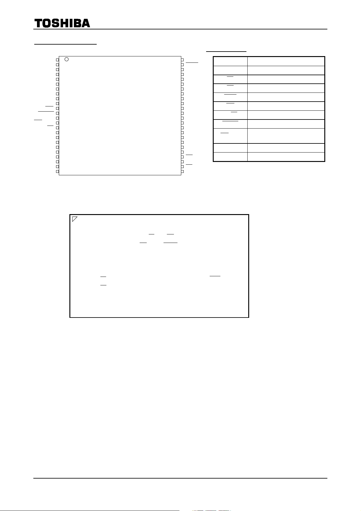
PIN ASSIGNMENT
(TOP VIEW)
…………TC58FVT641/B641FT PIN NAMES
RESET
/ACCWP
1 48
A15
2 47
A14
3 46
A13
4 45
A12
5 44
A11
6 43
A10
7 42
A9
8 41
A8
9 40
A19
10 39
A20
11 38
WE
12 37
13 36
A21
14 35
15 34
BY/RY
16 33
A18
17 32
A17
18 31
A7
19 30
A6
20 29
A5
21 28
A4
22 27
A3
23 26
A2
24 25
A1
A16
BYTE
VSS
DQ15/A-1
DQ7
DQ14
DQ6
DQ13
DQ5
DQ12
DQ4
DD
V
DQ11
DQ3
DQ10
DQ2
DQ9
DQ1
DQ8
DQ0
OE
SS
V
CE
A0
A-1, A0~A21 Address Input
DQ0~DQ15 Data Input/Output
Chip Enable Input
CE
Output Enable Input
OE
BYTE Word/Byte Select Input
WE Write Enable Input
BY/RY Ready/Busy Output
Hardware Reset Input
RESET
/ACCWP
VDD Power Supply
VSS Ground
…………TC58FVT641/B641XB
1 2 3 4 5 6 7 8
A NC NC NC NC
B NC NC NC
C A3 A7
D A4 A17 /ACCWP RESET A8 A12
E A2 A6 A18 A21 A10 A14
F A1 A5 A20 A19 A11 A15
G A0 DQ0 DQ2 DQ5 DQ7 A16
H CΕ DQ8 DQ10 DQ12 DQ14 BYTE
J OE DQ9 DQ11 VDD DQ13 DQ15
K VSS DQ1 DQ3 DQ4 DQ6 VSS
L NC NC NC NC
M NC NC NC NC
BY/RY
WE
A9 A13
Write Protect /
Program Acceleration Input
2001-09-06 2/53
Page 3
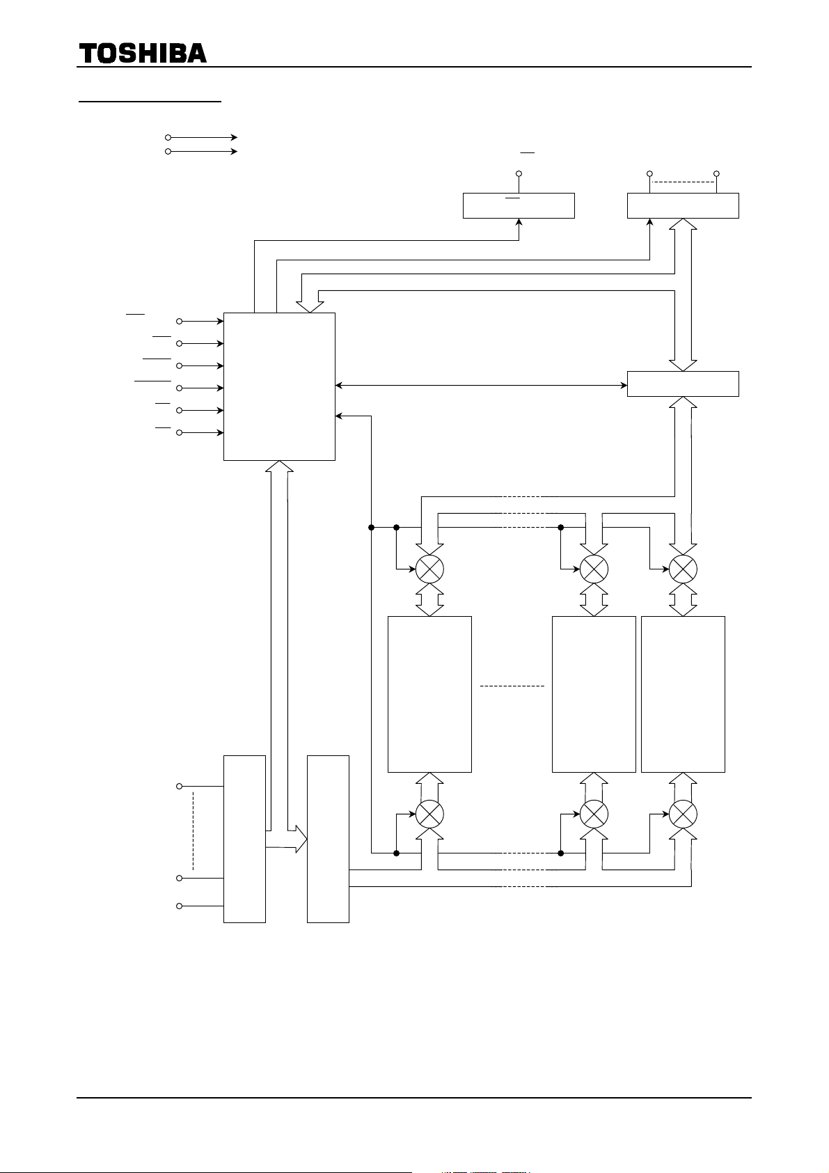
BLOCK DIAGRAM
V
DD
V
SS
TC58FVT641/B641FT/XB-70,-10
DQ0 BY/RY
DQ15
/ACCWP
WE
BYTE
RESET
CE
OE
Control Circuit
Command Register
BY/RY Buffer
I/O Buffer
Data Latch
Memory Cell
Array
Bank 16
A0
A21
A-1
Address Buffer
Memory Cell
Array
Bank 0
Address Latch
Memory Cell
Array
Bank 15
2001-09-06 3/53
Page 4
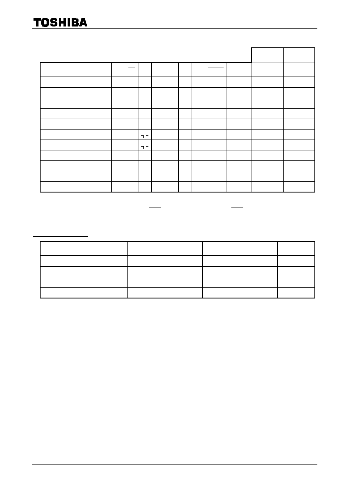
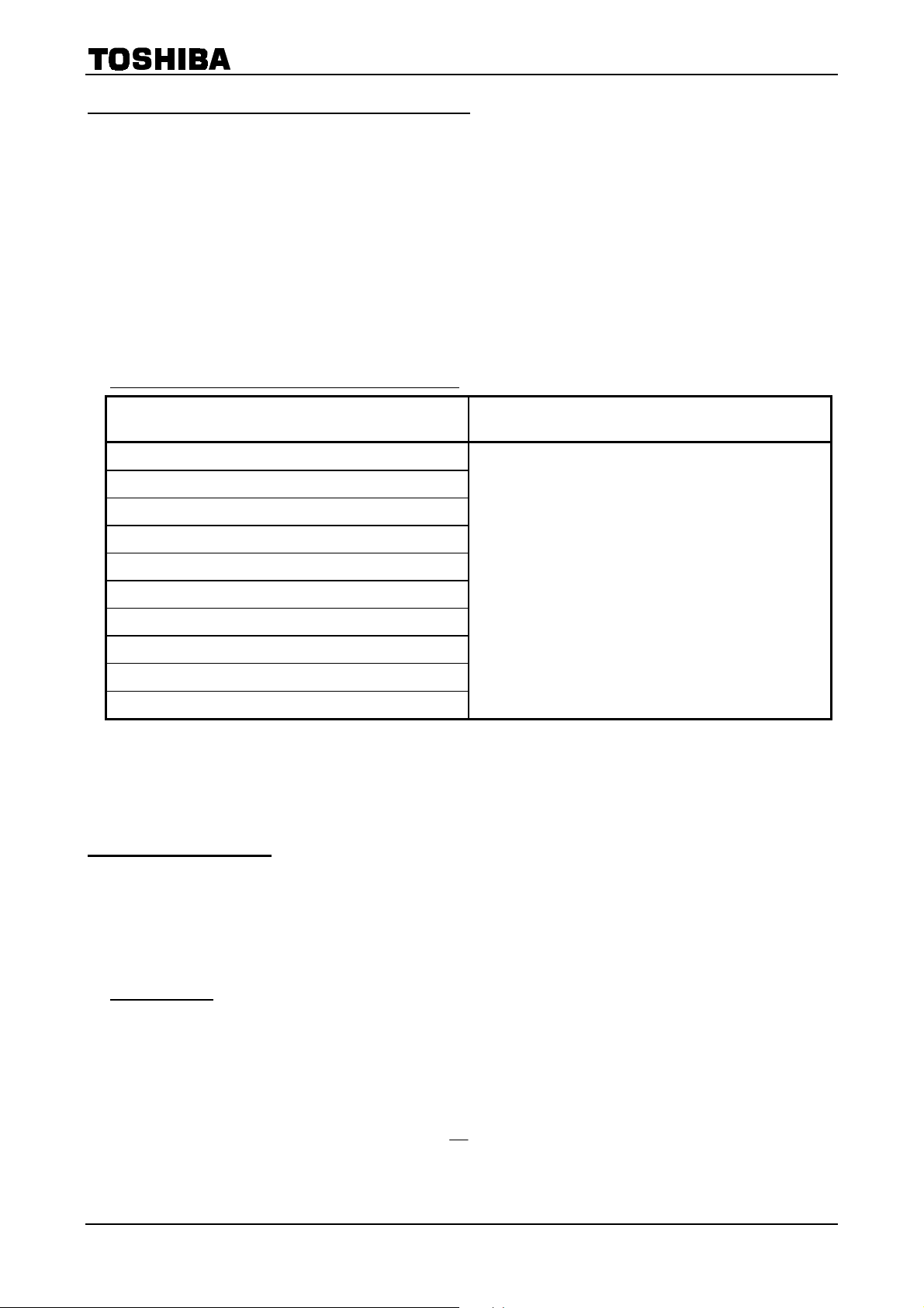
MODE SELECTION
BYTE MODE WORD MODE
TC58FVT641/B641FT/XB-70,-10
MODE
Read L L H A9 A6 A1 A0 H * D
ID Read (Manufacturer Code)
ID Read (Device Code)
Standby
Output Disable
Write L H
Block Protect 1 L VID
Verify Block Protect L L H VID L H L H * Code Code
Temporary Block Unprotect * * * * * * * VID * * *
Hardware Reset / Standby
Boot Block Protect * * * * * * * * L * *
Notes: * = VIH or VIL, L = VIL, H = VIH
(1) DQ8~DQ14 are High-Z and DQ15/A-1 is Address Input in Byte Mode.
Addresses are A21~A0 in Word Mode (
(2) Pulse input
CE OE
L L H VID L L L H * Code Code
L L H VID L L H H * Code Code
H * * * * * * H * High-Z High-Z
* H H * * * * * * High-Z High-Z
* * * * * * * L * High-Z High-Z
WE A9 A6 A1 A0
(2)
A9 A6 A1 A0 H * D
(2)
VID L H L H * * *
BYTE = VIH), A21~A-1 in Byte Mode ( BYTE = VIL).
RESET
/ACCWP
DQ0~DQ7
(1)
DQ0~DQ15
D
OUT
D
IN
OUT
IN
ID CODE TABLE
(3)
(1)
CODE TYPE A21~A12 A6 A1 A0 CODE (HEX)
Manufacturer Code * L L L 0098H
Device Code
Verify Block Protect BA
Notes: * = VIH or VIL, L = VIL, H = VIH
(1) DQ8~DQ14 are High-Z and DQ15/A-1 is Address Input in Byte Mode.
(2) BA: Block Address
(3) 0001H - Protected Block
0000H - Unprotected Block
TC58FVT641 * L L H 0093H
TC58FVB641 * L L H 0095H
(2)
L H L Data
2001-09-06 4/53
Page 5
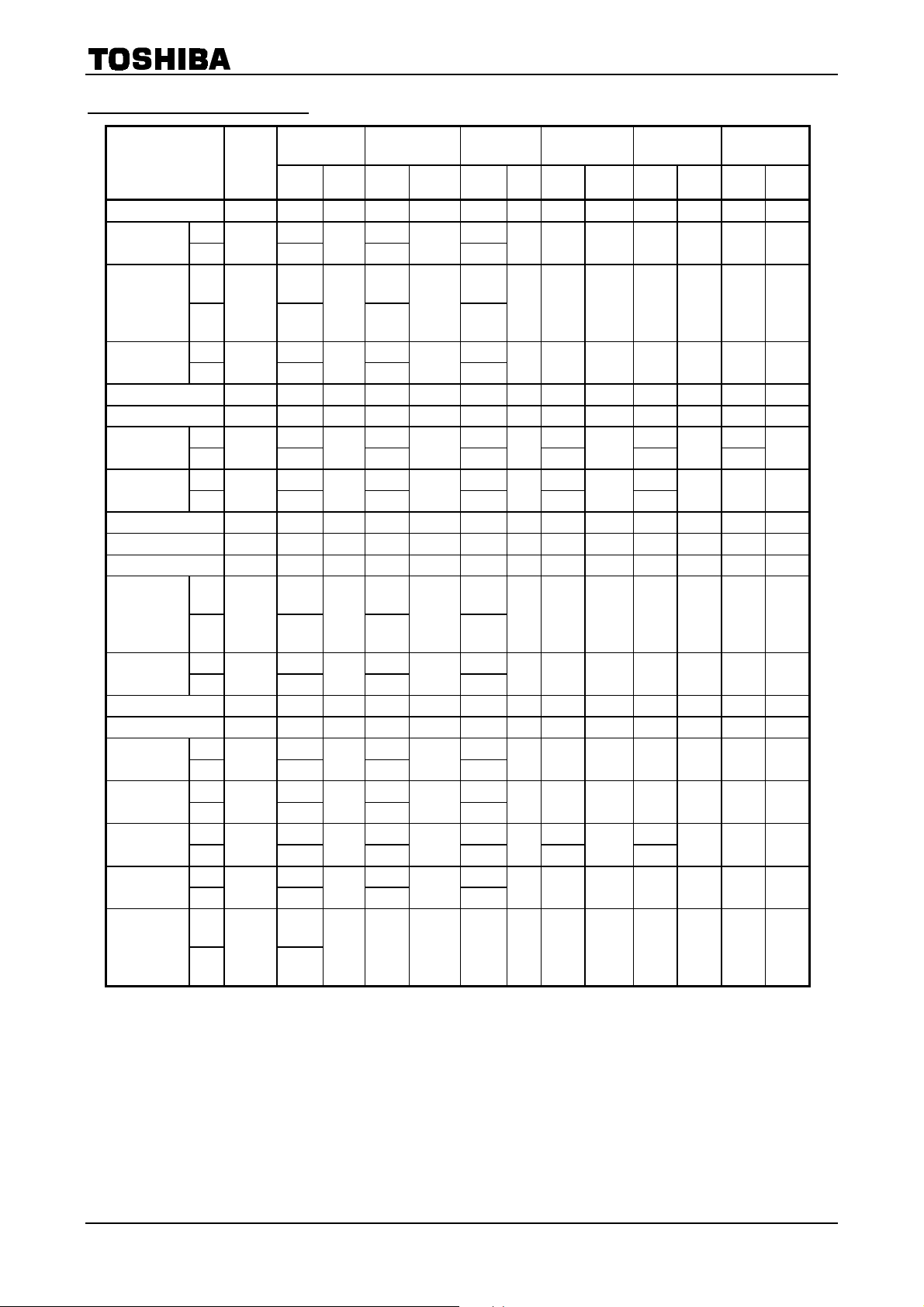
COMMAND SEQUENCES
TC58FVT641/B641FT/XB-70,-10
BUS
COMMAND
SEQUENCE
Read/Reset 1 XXXH F0H
Read/Reset
ID Read
Auto-Program
Program Suspend 1 BK
Program Resume 1 BK
Auto Chip
Erase
Auto Block
Erase
Block Erase Suspend 1 BK
Block Erase Resume 1 BK
Bloc k Protec t 2 4 XXXH 60H BPA
Verify Block
Protect
Fast Program
Set
Fast P rogram 2 XXXH A0H PA
Fast Program R eset 2 XXXH 90H XXXH F0H
Hidden ROM
Mode Entry
Hidden ROM
Program
Hidden ROM
Erase
Hidden ROM
Mode Exit
Query
Command
WRITE
CYCLES
REQ’D
Word 555H 2AAH 555H
Byte
Word 555H 2AAH
Byte
Word 555H 2AAH 555H
Byte
Word 555H 2AAH 555H 555H 2AAH 555H
Byte
Word 555H 2AAH 555H 555H 2AAH
Byte
Word 555H 2AAH
Byte
Word 555H 2AAH 555H
Byte
Word 555H 2AAH 555H
Byte
Word 555H 2AAH 555H
Byte
Word 555H 2AAH 555H 555H 2AAH
Byte
Word 555H 2AAH 555H
Byte
Word
Byte
3
3
4
6
6
3
3
3
4
6
4
2
FIRST BUS
WRITE CYCLE
Addr. Data Addr. Data Addr. Data Addr. Data Addr. Data Addr. Data
AAAH
AAAH
AAAH
AAAH
AAAH
AAAH
AAAH
AAAH
AAAH
AAAH
AAAH
BK
BK
AAH
AAH
AAH
(3)
B0H
(3)
30H
AAH
AAH
(3)
B0H
(3)
30H
AAH
AAH
AAH
AAH
AAH
AAH
(3)
+
55H
(3)
+
AAH
98H CA
SECOND BUS
WRITE CYCLE
555H
555H
555H
555H
555H
555H
555H
555H
555H
555H
555H
55H
55H
55H
55H
55H
(9)
60H XXXH 40H BPA
55H
55H
(6)
PD
55H
55H
55H
55H
(11)
CD
THIRD BUS
WRITE CYCLE
AAAH
(3)
BK
+
555H
(3)
BK
+
AAAH
AAAH
AAAH
AAAH
(3)
+
BK
555H
(3)
+
BK
AAAH
AAAH
(7)
(13)
AAAH
AAAH
AAAH
AAAH
(12)
FOURTH BUS
WRITE CYCLE
F0H RA
90H IA
A0H PA
80H
80H
90H BPA
20H
88H
A0H PA
80H
90H XXXH 00H
(1)
(4)
(6)
AAAH
AAAH
(6)
AAAH
RD
ID
PD
(9)
BPD
(9)
BPD
PD
AAH
AAH
AAH
FIFTH BUS
WRITE CYCLE
(2)
(5)
(7)
55H
555H
55H BA
555H
(10)
(10)
(7)
55H BA
555H
SIXTH BUS
WRITE CYCLE
AAAH
(8)
(8)
Notes: The system should generate the following address patterns:
Word Mode: 555H or 2AAH on address pins A10~A0
Byte Mode: AAAH or 555H on address pins A10~A-1
DQ8~DQ15 are ignored in Word Mode.
(1) RA: Read Address
(2) RD: Read Data
(3) BK: Bank Address = A21~A15
(4) IA: Bank Address and ID Read Address (A6, A1, A0)
Bank Address = A21~A15
Manufacturer Code = (0, 0, 0)
Device Code = (0, 0, 1)
(5) ID: ID Data
(6) PA: Program Address
(7) PD: Program Data
(8) BA: Block Address = A21~A12
(9) BPA: Block Address and ID Read Address (A6, A1, A0)
Block Address = A21~A12
ID Read Address = (0, 1, 0)
(10) BPD: Verify Data
(11) CA: CFI Address
(12) CD: CFI Data
(13) F0H: 00H is valid too
10H
30H
30H
2001-09-06 5/53
Page 6
TC58FVT641/B641FT/XB-70,-10
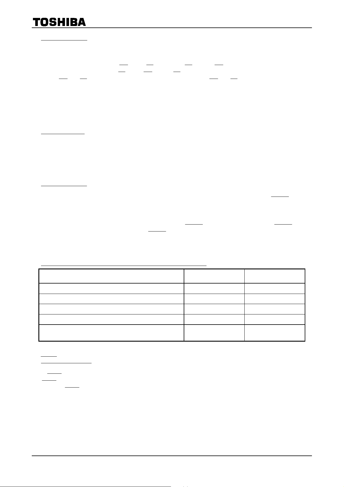
SIMULTANEOUS READ/WRITE OPERATION
The TC58FVT641/B641 features a Simultaneous Read/Write operation. The Simultaneous Read/Write operation
enables the device to simultaneously write data to or erase data from a bank while reading data from another bank.
The TC58FVT641/B641 has a total of seventeen banks: 1 bank of 0.5 Mbits, 1 bank of 3.5 Mbits and 15 banks of 4
Mbits. Banks can be switched between using the bank addresses (A21~A15). For a description of bank blocks and
addresses, please refer to the Block Address Table and Block Size Table.
The Simultaneous Read/Write operation cannot perform multiple operations within a single bank. The table
below shows the operation modes in which simultaneous operation can be performed.
Note that during Auto-Program execution or Auto Block Erase operation, the Simultaneous Read/Write operation
cannot read data from addresses in the same bank which have not been selected for operation. Data from these
addresses can be read using the Program Suspend or Erase Suspend function, however.
SIMULTANEOUS READ/WRITE OPERATION
STATUS OF BANK ON WHICH OPERATION IS BEING
PERFORMED
Read Mode
ID Read Mode
Auto-Program Mode
Fast Program Mode
Program Suspend Mode
Auto Block Erase Mode
Auto Multiple Block Erase Mode
Erase Suspend Mode
Program Suspend during Erase Suspend
CFI Mode
(1) Only Command Mode is valid.
(2) Including times when Acceleration Mode is in use.
(3) If the selected blocks are spread across all nine banks, simultaneous operation cannot be carried out.
(1)
(2)
(3)
STATUS OF OTHER BANKS
Read Mode
OPERATION MODES
In addition to the Read, Write and Erase Modes, the TC58FVT641/B641 features many functions including block
protection and data polling. When incorporating the device into a deign, please refer to the timing charts and
flowcharts in combination with the description below.
READ MODE
To read data from the memory cell array, set the device to Read Mode. In Read Mode the device can perform
high-speed random access as asynchronous ROM.
The device is automatically set to Read Mode immediately after power-on or on completion of automatic
operation. A software reset releases ID Read Mode and the lock state which the device enters if automatic
operation ends abnormally, and sets the device to Read Mode. A hardware reset terminates operation of the
device and resets it to Read Mode. When reading data without changing the address immediately after
power-on, either input a hardware Reset or change
CE from H to L.
2001-09-06 6/53
Page 7

TC58FVT641/B641FT/XB-70,-10
ID Read Mode
ID Read Mode is used to read the device maker code and device code. The mode is useful in that it allows
EPROM programmers to identify the device type automatically.
ID read can be executed in two ways, as follows:
(1) Applying V
This method is used mainly by EPROM programmers. Applying V
Mode, outputting the maker code from address 00H and the device code from address 01H. Releasing V
from A9 returns the device to Read Mode. With this method all banks are set to ID Read Mode; thus,
simultaneous operation cannot be performed.
(2) Input command sequence
With this method simultaneous operation can be performed. Inputting an ID Read command sets the
specified bank to ID Read Mode. Banks are specified by inputting the bank address (BK) in the third Bus
Write cycle of the Command cycle. To read an ID code, the bank address as well as the ID read address must
be specified. The maker code is output from address BK + 00; the device code is output from address BK +
01. From other banks data are output from the memory cells. Inputting a Reset command releases ID Read
Mode and returns the device to Read Mode.
Access time in ID Read Mode is the same as that in Read Mode. For a list of the codes, please refer to the
ID Code Table.
Standby Mode
There are two ways to put the device into Standby Mode.
(1) Control using
With the device in Read Mode, input V
Mode and the current will be reduced to the standby current (I
process of performing simultaneous operation, the device will not enter Standby Mode but will instead
cause the operating current to flow.
(2) Control using
With the device in Read Mode, input V
current will be reduced to the standby current (I
simultaneous operation, this method will terminate the current operation and set the device to Standby
Mode. This is a hardware reset and is described later.
In Standby Mode DQ is put in High-Impedance state.
Auto-Sleep Mode
This function suppresses power dissipation during reading. If the address input does not change for 150 ns,
the device will automatically enter Sleep Mode and the current will be reduced to the standby current (I
However, if the device is in the process of performing simultaneous operation, the device will not enter Standby
Mode but will instead cause the operating current to flow. Because the output data is latched, data is output in
Sleep Mode. When the address is changed, Sleep Mode is automatically released, and data from the new
address is output.
Output Disable Mode
Inputting V
to A9
ID
to A9 sets the device to ID Read
ID
CE and RESET
± 0.3 V to CE and RESET . The device will enter Standby
DD
). However, if the device is in the
DDS1
RESET only
± 0.3 V to RESET . The device will enter Standby Mode and the
SS
). Even if the device is in the process of performing
DDS1
to OE disables output from the device and sets DQ to High-Impedance.
IH
DDS2
ID
).
2001-09-06 7/53
Page 8
TC58FVT641/B641FT/XB-70,-10
Command Write
The TC58FVT641/B641 uses the standard JEDEC control commands for a single-power supply E
Command Write is executed by inputting the address and data into the Command Register. The command is
written by inputting a pulse to
written by inputting a pulse to
either
input and DQ8~DQ15 are ignored.
and enter Read Mode. If an undefined command is input, the Command Register will be reset and the device
will enter Read Mode.
WE or CE . The data is latched on the rising edge of either WE or CE . DQ0~DQ7 are valid for data
To abort input of the command sequence use the Reset command. The device will reset the Command Register
WE with CE = VIL and OE = VIH ( WE control). The command can also be
CE with WE = VIL ( CE control). The address is latched on the falling edge of
Software Reset
Apply a software reset by inputting a Read/Reset command. A software reset returns the device from ID Read
Mode or CFI Mode to Read Mode, releases the lock state if automatic operation has ended abnormally, and
clears the Command Register.
Hardware Reset
A hardware reset initializes the device and sets it to Read Mode. When a pulse is input to
the device abandons the operation which is in progress and enters Read Mode after t
hardware reset is applied during data overwriting, such as a Write or Erase operation, data at the address or
block being written to at the time of the reset will become undefined.
After a hardware reset the device enters Read Mode if
The DQ pins are High-Impedance when
operations and input of any command are allowed.
RESET = VIL. After the device has entered Read Mode, Read
RESET = VIH or Standby Mode if RESET = VIL.
READY
Comparison between Software Reset and Hardware Reset
2
PROM. A
RESET for tRP,
. Note that if a
ACTION SOFTWARE RESET HARDWARE RESET
Releases ID Read Mode or CFI Mode. True True
Clears the Command Register. True True
Releases the lock state if automatic operation has ended abnormally. True True
Stops any automatic operation which is in progress. False True
Stops any operation other than the above and returns the device to
Read Mode.
/Word Mode
BYTE
BYTE is used select Word Mode (16 bits) or Byte Mode (8 bits) for the TC58FVT641/B641. If VIH is input to
BYTE , the device will operate in Word Mode. Read data or write commands using DQ0~DQ15. When VIL is
input to
DQ8~DQ14 will become High-Impedance.
BYTE , read data or write commands using DQ0~DQ7. DQ15/A-1 is used as the lowest address.
False True
2001-09-06 8/53
Page 9

TC58FVT641/B641FT/XB-70,-10
Auto-Program Mode
The TC58FVT641/B641 can be programmed in either byte or word units. Auto-Program Mode is set using the
Program command. The program address is latched on the falling edge of the
on the rising edge of the fourth Bus Write cycle (with
of the
executed by the chip. The device status during programming is indicated by the Hardware Sequence flag. To
read the Hardware Sequence flag, specify the address to which the Write is being performed
cannot be accepted. To terminate execution, use a hardware reset. Note that if the Auto-Program operation is
terminated in this manner, the data written so far is invalid.
rising edge of the
return to Read Mode. The device status is indicated by the Hardware Sequence flag. Either a Reset command or
a hardware reset is required to return the device to Read Mode after a failure. If a programming operation fails,
the block which contains the address to which data could not be programmed should not be used.
cells which contain 0s. If this is attempted, execution of Auto Program will fail. This is a user error, not a device
error. A cell containing 0 must be erased in order to set it to 1.
WE signal in the fourth Bus Write cycle. The Program and Program Verify commands are automatically
During Auto Program execution, a command sequence for the bank on which execution is being performed
Any attempt to program a protected block is ignored. In this case the device enters Read Mode 3 µs after the
WE signal in the fourth Bus Write cycle.
If an Auto-Program operation fails, the device remains in the programming state and does not automatically
The device allows 0s to be programmed into memory cells which contain a 1. 1s cannot be programmed into
WE control). Auto programming starts on the rising edge
Fast Program Mode
Fast Program is a function which enables execution of the command sequence for the Auto Program to be
completed in two cycles. In this mode the first two cycles of the command sequence, which normally requires
four cycles, are omitted. Writing is performed in the remaining two cycles. To execute Fast Program, input the
Fast Program command. Write in this mode uses the Fast Program command but operation is the same at that
for ordinary Auto-Program. The status of the device is indicated by the Hardware Sequence flag and read
operations can be performed as usual. To exit this mode, the Fast Program Reset command must be input.
When the command is input, the device will return to Read Mode.
Acceleration Mode
The TC58FVT641/B641 features Acceleration Mode which allows write time to be reduced. Applying V
WP or ACC automatically sets the device to Acceleration Mode. In Acceleration Mode, Block Protect Mode
changes to Temporary Block Unprotect Mode. Write Mode changes to Fast Program Mode. Modes are switched
by the
Program Mode. Operation of Write is the same as in Auto-Program Mode. Removing V
terminates Acceleration Mode.
/ACCWP signal; thus, there is no need for a Temporary Block Unprotect operation or to set or reset Fast
WE signal and data is latched
.
from /ACCWP
ACC
ACC
to
2001-09-06 9/53
Page 10

TC58FVT641/B641FT/XB-70,-10
Program Suspend/Resume Mode
Program Suspend is used to enable Data Read by suspending the Write operation. The device accepts a
Program Suspend command in Write Mode (including Write operations performed during Erase Suspend) but
ignores the command in other modes. When the command is input, the address of the bank on which Write is
being performed must be specified. After input of the command, the device will enter Program Suspend Read
Mode after t
During Program Suspend, Cell Data Read, ID Read and CFI Data Read can be performed. When Data Write
is suspended, the address to which Write was being performed becomes undefined. ID Read and CFI Data Read
are the same as usual.
After completion of Program Suspend input a Program Resume command to return to Write Mode. When
inputting the command, specify the address of the bank on which Write is being performed. If the ID Read or
CFI Data Read functions is being used, abort the function before inputting the Resume command. On receiving
the Resume command, the device returns to Write Mode and resumes outputting the Hardware Sequence flag
for the bank to which data is being written.
Program Suspend can be run in Fast Program Mode or Acceleration Mode. However, note that when running
Program Suspend in Acceleration Mode, V
Auto Chip Erase Mode
The Auto Chip Erase Mode is set using the Chip Erase command. An Auto Chip Erase operation starts on the
rising edge of
verified as erased by the chip. The device status is indicated by the Hardware Sequence flag.
Command input is ignored during an Auto Chip Erase. A hardware reset can interrupt an Auto Chip Erase
operation. If an Auto Chip Erase operation is interrupted, it cannot be completed correctly. Hence an additional
Erase operation must be performed.
Any attempt to erase a protected block is ignored. If all blocks are protected, the Auto Erase operation will not
be executed and the device will enter Read mode 100 µs after the rising edge of the
cycle.
If an Auto Chip Erase operation fails, the device will remain in the erasing state and will not return to Read
Mode. The device status is indicated by the Hardware Sequence flag. Either a Reset command or a hardware
reset is required to return the device to Read Mode after a failure.
In this case it cannot be ascertained which block the failure occurred in. Either abandon use of the device
altogether, or perform a Block Erase on each block, identify the failed block, and stop using it. The host
processor must take measures to prevent subsequent use of the failed block.
.
SUSP
must not be released.
ACC
WE in the sixth bus cycle. All memory cells are automatically preprogrammed to 0, erased and
WE signal in the sixth bus
2001-09-06 10/53
Page 11

TC58FVT641/B641FT/XB-70,-10
Auto Block Erase / Auto Multi-Block Erase Modes
The Auto Block Erase Mode and Auto Multi-Block Erase Mode are set using the Block Erase command. The
block address is latched on the falling edge of the
soon as the Erase Hold Time (t
are erased, the sixth Bus Write cycle is repeated with each block address and Auto Block Erase command being
input within the Erase Hold Time (this constitutes an Auto Multi-Block Erase operation). If a command other
than an Auto Block Erase command or Erase Suspend command is input during the Erase Hold Time, the
device will reset the Command Register and enter Read Mode. The Erase Hold Time restarts on each successive
rising edge of
preprogrammed to 0, erased and verified as erased by the chip. The device status is indicated by the setting of
the Hardware Sequence flag. When the Hardware Sequence flag is read, the addresses of the blocks on which
auto-erase operation is being performed must be specified. If the selected blocks are spread across all nine
banks, simultaneous operation cannot be carried out.
All commands (except Erase Suspend) are ignored during an Auto Block Erase or Auto Multi-Block Erase
operation. Either operation can be aborted using a Hardware Reset. If an auto-erase operation is interrupted, it
cannot be completed correctly; therefore, a further erase operation is necessary to complete the erasing.
Any attempt to erase a protected block is ignored. If all the selected blocks are protected, the auto-erase
operation is not executed and the device returns to Read Mode 100 µs after the rising edge of the
the last bus cycle.
If an auto-erase operation fails, the device remains in Erasing state and does not return to Read Mode. The
device status is indicated by the Hardware Sequence flag. After a failure either a Reset command or a Hardware
Reset is required to return the device to Read Mode. If multiple blocks are selected, it will not be possible to
ascertain the block in which the failure occurred. In this case either abandon use of the device altogether, or
perform a Block Erase on each block, identify the failed block, and stop using it. The host processor must take
measures to prevent subsequent use of the failed block.
WE . Once operation starts, all memory cells in the selected block are automatically
) has elapsed after the rising edge of the WE signal. When multiple blocks
BEH
Erase Suspend / Erase Resume Modes
Erase Suspend Mode suspends Auto Block Erase and reads data from or writes data to an unselected block.
The Erase Suspend command is allowed during an auto block erase operation but is ignored in all other
oreration modes. When the command is input, the address of the bank on which Erase is being performed must
be specified.
In Erase Suspend Mode only a Read, Program or Resume command can be accepted. If an Erase Suspend
command is input during an Auto Block Erase, the device will enter Erase Suspend Read Mode after t
device status (Erase Suspend Read Mode) can be verified by checking the Hardware Sequence flag. If data is
read consecutively from the block selected for Auto Block Erase, the DQ2 output will toggle and the DQ6 output
will stop toggling and
Inputting a Write command during an Erase Suspend enables a Write to be performed to a block which has
not been selected for the Auto Block Erase. Data is written in the usual manner.
To resume the Auto Block Erase, input an Erase Resume command. On input of the command, the address of
the bank on which the Write was being performed must be specified. On receiving an Erase Resume command,
the device returns to the state it was in when the Erase Suspend command was input. If an Erase Suspend
command is input during the Erase Hold Time, the device will return to the state it was in at the start of the
Erase Hold Time. At this time more blocks can be specified for erasing. If an Erase Resume command is input
during an Auto Block Erase, Erase resumes. At this time toggle output of DQ6 resumes and 0 is output on
BY/RY .
BY/RY will be set to High-Impedance.
WE signal in the sixth bus cycle. The block erase starts as
WE signal in
SUSE
. The
2001-09-06 11/53
Page 12

TC58FVT641/B641FT/XB-70,-10
BLOCK PROTECTION
Block Protection is a function for disabling writing and erasing specific blocks. Block protection can be carried
out in two ways: by supplying a high voltage (V
voltage and a command sequence (see Block protection 2).
(1) Block protection 1
Specify a device block address and make the following signal settings A9 =
= A0 = A6 = V
protection circuit. Block protection can be verified using the Verify Block Protect command. Inputting V
on
OE sets the device to Verify Mode. 01H is output if the block is protected and 00H is output if the block
is unprotected. If block protection was unsuccessful, the operation must be repeated. Releasing V
and
OE terminates this mode.
(2) Block protection 2
Applying V
first cycle of the command sequence is the Set-up command. In the second cycle, the Block Protect command
is input, in which a block address and A1 = V
block protection circuit. There is a wait of t
necessary during this time. In the third cycle the Verify Block Protect command is input. This command
verifies the write to the block protection circuit. Read is performed in the fourth cycle. If the protection
operation is complete, 01H is output. If a value other than 01H is output, block protection is not complete
and the Block Protect command must be input again. Removing the V
mode.
. Now when a pulse is input to WE for t
IL
to RESET and inputting the Block Protect 2 command also performs block protection. The
ID
Temporary Block Unprotection
The TC58FVT641/B641 has a temporary block unprotection feature which disables block protection for all
protected blocks. Unprotection is enabled by applying V
can be performed on all blocks except the boot blocks which have been protected by the Boot Block Protect
operation. The device returns to its previous state when V
previously protected blocks will be protected again.
Verify Block Protect
The Verify Block Protect command is used to ascertain whether a block is protected or unprotected.
Verification is performed either by inputting the Verify Block Protect command or by applying V
as for ID Read Mode, and setting the block address = A0 = A6 = V
is output. If the block is unprotected, 00H is output.
Boot Block Protection
Boot block protection temporarily protects certain boot blocks using a method different from ordinary block
protection. Neither V
on
bottom boot blocks are BA0 and BA1. Inputting V
necessary to protect these blocks, the ordinary Block Protection Mode must be used.
/ACCWP . The target blocks are the two pairs of boot blocks. The top boot blocks are BA133 and BA134; the
nor a command sequence is required. Protection is performed simply by inputting VIL
ID
) to the device (see Block protection 1) or by supplying a high
ID
OE = VID, A1 = VIH and CE
, the device will start to write to the block
PPLH
from A9
ID
and A0 = A6 = VIL are input. Now the device writes to the
IH
until this write is completed; however, no intervention is
PPLH
input from RESET exits this
ID
to the RESET pin. Now Write and Erase operations
ID
is removed from the RESET pin. That is,
ID
to the A9 pin,
ID
and A1 = VIH. If the block is protected, 01H
IL
on /ACCWP releases the mode. From now on, if it is
IH
IL
2001-09-06 12/53
Page 13
TC58FVT641/B641FT/XB-70,-10
Hidden ROM Area
The TC58FVT641/B641 features a 64-Kbyte hidden ROM area which is separate from the memory cells. The
area consists of one block. Data Read, Write and Protect can be performed on this block. Because Protect cannot
be released, once the block is protected, data in the block cannot be overwritten.
The hidden ROM area is located in the address space indicated in the HIDDEN ROM AREA ADDRESS
TABLE. To access the Hidden ROM area, input a Hidden ROM Mode Entry command. The device now enters
Hidden ROM Mode, allowing Read, Write, Erase and Block Protect to be executed. Write and Erase operations
are the same as auto operations except that the device is in Hidden ROM Mode. However, regarding write
operation, Accelaration mode can not be performed during Hidden ROM Mode. To protect the hidden ROM area,
use the block protection function. The operation of Block Protect here is the same as a normal Block Protect
except that V
released, even using the temporary block unprotection function. Use Block Protect carefully. Note that in
Hidden ROM Mode, simultaneous operation cannot be performed. Therefore, do not attempt to access areas
other than the hidden ROM area.
To exit Hidden ROM Mode, use the Hidden ROM Mode Exit command. This will return the device to Read
Mode.
HIDDEN ROM AREA ADDRESS TABLE
rather than VID is input to RESET . Once the block has been protected, protection cannot be
IH
TYPE
TC58FVT641 TOP BOOT BLOCK 7F0000H~7FFFFFH 64 Kbytes 3F8000H~3FFFFFH 32 Kwords
TC58FVB641 BOTTOM BOOT BLOCK 000000H~00FFFFH 64 Kbytes 000000H~007FFFH 32 Kwords
BOOT BLOCK
ARCHITECTURE
ADDRESS RANGE SIZE ADDRESS RANGE SIZE
BYTE MODE WORD MODE
2001-09-06 13/53
Page 14
TC58FVT641/B641FT/XB-70,-10
COMMON FLASH MEMORY INTERFACE (CFI)
The TC58FVT641/B641 conforms to the CFI specifications. To read information from the device, input the
Query command followed by the address. In Word Mode DQ8~DQ15 all output 0s. To exit this mode, input the
Reset command.
CFI CODE TABLE
ADDRESS A6~A0 DATA DQ15~DQ0 DESCRIPTION
10H
11H
12H
13H
14H
15H
16H
17H
18H
19H
1AH
1BH 0027H
1CH 0036H
1DH 0000H VPP (min) voltage
1EH 0000H VPP (max) voltage
1FH 0004H Typical time-out per single byte/word write (2N µs)
20H 0000H Typical time-out for minimum size buffer write (2N µs)
0051H
0052H
0059H
0002H
0000H
0040H
0000H
0000H
0000H
0000H
0000H
ASCII string “QRY”
Primary OEM command set
2: AMD/FJ standard type
Address for primary extended table
Alternate OEM command set
0: none exists
Address for alternate OEM extended table
V
(min) (Write/Erase)
DD
DQ7~DQ4: 1 V
DQ3~DQ0: 100 mV
(max) (Write/Erase)
V
DD
DQ7~DQ4: 1 V
DQ3~DQ0: 100 mV
21H 000AH Typical time-out per individual block erase (2N ms)
22H 0000H Typical time-out for full chip erase (2N ms)
23H 0005H Maximum time-out for byte/word write (2N times typical)
24H 0000H Maximum time-out for buffer write (2N times typical)
25H 0004H Maximum time-out per individual block erase (2N times typical)
26H 0000H Maximum time-out for full chip erase (2N times typical)
27H 0017H Device Size (2N byte)
28H
29H
2AH
2BH
0002H
0000H
0000H
0000H
Flash device interface description
2: ×8/×16
Maximum number of bytes in multi-byte write (2
N
)
2001-09-06 14/53
Page 15
TC58FVT641/B641FT/XB-70,-10
ADDRESS A6~A0 DATA DQ15~DQ0 DESCRIPTION
2CH 0002H Number of erase block regions within device
2DH
2EH
2FH
30H
31H
32H
33H
34H
40H
41H
42H
43H 0031H Major version number, ASCII
44H 0031H Minor version number, ASCII
45H 0000H
46H 0002H
47H 0001H
0007H
0000H
0020H
0000H
007EH
0000H
0000H
0001H
0050H
0052H
0049H
Erase Block Region 1 information
Bits 0~15: y = block number
Bits 16~31: z = block size
(z × 256 bytes)
Erase Block Region 2 information
ASCII string “PRI”
Address-Sensitive Unlock
0: Required
1: Not required
Erase Suspend
0: Not supported
1: For Read-only
2: For Read & Write
Block Protect
0: Not supported
X: Number of blocks per group
Block Temporary Unprotect
48H 0001H
49H 0004H Block Protect/Unprotect scheme
4AH 0001H
4BH 0000H
4CH 0000H
4DH 0085H
4EH 0095H
4FH 000XH
50H 0001H
0: Not supported
1: Supported
Simultaneous operation
0: Not supported
1: Supported
Burst Mode
0: Not supported
Page Mode
0: Not supported
(min) voltage
V
ACC
DQ7~DQ4: 1 V
DQ3~DQ0: 100 mV
(max) voltage
V
ACC
DQ7~DQ4: 1 V
DQ3~DQ0: 100 mV
Top/Bottom Boot Block Flag
2: TC58FVB641
3: TC58FVT641
Program Suspend
0: Not supported
1: Supported
2001-09-06 15/53
Page 16
TC58FVT641/B641FT/XB-70,-10
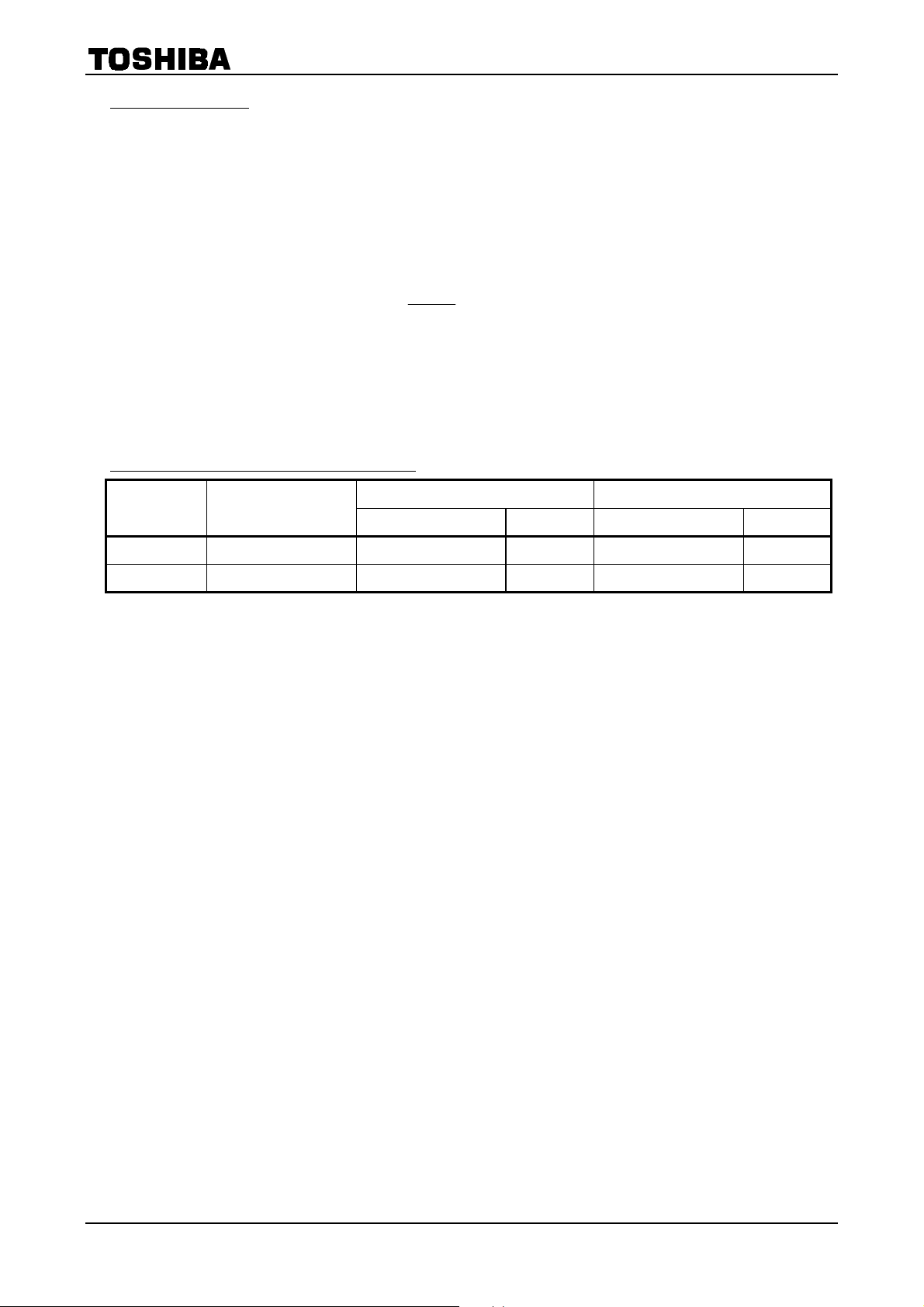
HARDWARE SEQUENCE FLAGS
The TC58FVT641/B641 has a Hardware Sequence flag which allows the device status to be determined during an
auto mode operation. The output data is read out using the same timing as that used when
Read Mode. The
BY/RY output can be either High or Low.
The device re-enters Read Mode automatically after an auto mode operation has been completed successfully. The
Hardware Sequence flag is read to determine the device status and the result of the operation is verified by
comparing the read-out data with the original data.
STATUS DQ7 DQ6 DQ5 DQ3 DQ2 BY/RY
CE = OE = VIL in
Auto Programming
Read in Program Suspend
Erase Hold Time
In Auto
Erase
In Progress
In Erase
Suspend
Auto Programming
Time Limit
Exceeded
Notes:DQ outputs cell data and BY/RY goes High-Impedence when the operation has been completed.
Auto Erase 0 Toggle 1 1 NA 0
Programming in Erase Suspend
DQ0 and DQ1 pins are reserved for future use.
0 is output on DQ0, DQ1 and DQ4.
(1) Data output from an address to which Write is being performed is undefined.
(2) Output when the block address selected for Auto Block Erase is specified and data is read from there.
During Auto Chip Erase, all blocks are selected.
(3) Output when a block address not selected for Auto Block Erase of same bank as selected block is specified and data is
read from there.
Auto Erase
Read
Programming
(1)
Data Data Data Data Data High-Z
Selected
Not-selected
Not-selected 0 Toggle 0 1 1 0
Not-selected Data Data Data Data Data High-Z
Not-selected
(2)
0 Toggle 0 0 Toggle 0
(3)
0 Toggle 0 0 1 0
Selected 0 Toggle 0 1 Toggle 0
Selected 1 1 0 0 Toggle High-Z
Selected
Toggle 0 0 1 0
7DQ
Toggle 0 0 Toggle 0
7DQ
Toggle 0 0 1 0
7DQ
Toggle 1 0 1 0
7DQ
Toggle 1 0 NA 0
7DQ
DQ7 ( polling)
DATA
During an Auto-Program or auto-erase operation, the device status can be determined using the data polling
function.
DATA polling begins on the rising edge of WE in the last bus cycle. In an Auto-Program operation,
DQ7 outputs inverted data during the programming operation and outputs actual data after programming has
finished. In an auto-erase operation, DQ7 outputs 0 during the Erase operation and outputs 1 when the Erase
operation has finished. If an Auto-Program or auto-erase operation fails, DQ7 simply outputs the data.
When the operation has finished, the address latch is reset. Data polling is asynchronous with the
signal.
OE
2001-09-06 16/53
Page 17

TC58FVT641/B641FT/XB-70,-10
DQ6 (Toggle bit 1)
The device status can be determined by the Toggle Bit function during an Auto-Program or auto-erase
operation. The Toggle bit begins toggling on the rising edge of
outputs a 0 or a 1 for each
has been completed, toggling stops and valid memory cell data can be read by subsequent reading. If the
operation fails, the DQ6 output toggles.
If an attempt is made to execute an Auto Program operation on a protected block, DQ6 will toggle for around
3 µs. It will then stop toggling. If an attempt is made to execute an auto erase operation on a protected block,
DQ6 will toggle for around 100 µs. It will then stop toggling. After toggling has stopped the device will return to
Read Mode.
OE access while CE = VIL while the device is busy. When the internal operation
DQ5 (internal time-out)
If the internal timer times out during a Program or Erase operation, DQ5 outputs a 1. This indicates that the
operation has not been completed within the allotted time.
Any attempt to program a 1 into a cell containing a 0 will fail (see Auto-Program Mode). In this case DQ5
outputs a 1. Either a hardware reset or a software Reset command is required to return the device to Read
Mode.
DQ3 (Block Erase timer)
The Block Erase operation starts 50 µs (the Erase Hold Time) after the rising edge of WE in the last
command cycle. DQ3 outputs a 0 for the duration of the Block Erase Hold Time and a 1 when the Block Erase
operation starts. Additional Block Erase commands can only be accepted during the Block Erase Hold Time.
Each Block Erase command input within the hold time resets the timer, allowing additional blocks to be marked
for erasing. DQ3 outputs a 1 if the Program or Erase operation fails.
DQ2 (Toggle bit 2)
DQ2 is used to indicate which blocks have been selected for Auto Block Erase or to indicate whether the
device is in Erase Suspend Mode.
If data is read continuously from the selected block during an Auto Block Erase, the DQ2 output will toggle.
Now 1 will be output from non-selected blocks; thus, the selected block can be ascertained. If data is read
continuously from the block selected for Auto Block Erase while the device is in Erase Suspend Mode, the DQ2
output will toggle. Because the DQ6 output is not toggling, it can be determined that the device is in Erase
Suspend Mode. If data is read from the address to which data is being written during Erase Suspend in
Programming Mode, DQ2 will output a 1.
BY/RY
(READY/ )
TC58FVT641/B641 has a BY/RY signal to indicate the device status to the host processor. A 0 (Busy state)
indicates that an Auto-Program or auto-erase operation is in progress. A 1 (Ready state) indicates that the
operation has finished and that the device can now accept a new command.
operation has failed.
BY/RY outputs a 0 after the rising edge of WE in the last command cycle.
During an Auto Block Erase operation, commands other than Erase Suspend are ignored.
1 during an Erase Suspend operation. The output buffer for the
allowing a wired-OR connection. A pull-up resistor must be inserted between V
BUSY
WE in the last bus cycle. DQ6 alternately
BY/RY outputs a 0 when an
BY/RY outputs a
BY/RY pin is an open-drain type circuit,
and the BY/RY pin.
DD
2001-09-06 17/53
Page 18

TC58FVT641/B641FT/XB-70,-10
DATA PROTECTION
The TC58FVT641/B641 includes a function which guards against malfunction or data corruption.
Protection against Program/Erase Caused by Low Supply Voltage
To prevent malfunction at power-on or power-down, the device will not accept commands while VDD is below
V
. In this state, command input is ignored.
LKO
If V
drops below V
DD
this case, Auto operation is not executed again when V
command need to be input to execute Auto operation again.
When V
DD
> V
, make up countermeasure to be input accurately command in system side please.
LKO
Protection against Malfunction Caused by Glitches
To prevent malfunction during operation caused by noise from the system, the device will not accept pulses
shorter than 3 ns (Typ.) input on
glitch is input to the device malfunction may occur.
The device uses standard JEDEC commands. It is conceivable that, in extreme cases, system noise may be
misinterpreted as part of a command sequence input and that the device will acknowledge it. Then, even if a
proper command is input, the device may not operate. To avoid this possibility, clear the Command Register
before command input. In an environment prone to system noise, Toshiba recommend input of a software or
hardware reset before command input.
Protection against Malfunction at Power-on
To prevent damage to data caused by sudden noise at power-on, when power is turned on with
V
the device does not latch the command on the first rising edge of WE or CE . Instead, the device
IL
automatically Resets the Command Register and enters Read Mode.
during an Auto Operation, the device will terminate Auto-Program execution. In
LKO
return to recommended VDD voltage Therefore,
DD
WE , CE or OE . However, if a glitch exceeding 3 ns (Typ.) occurs and the
WE = CE =
2001-09-06 18/53
Page 19

TC58FVT641/B641FT/XB-70,-10
ABSOLUTE MAXIMUM RATINGS
SYMBOL PARAMETER RANGE UNIT
VDD V
VIN Input Voltage −0.6~VDD + 0.5 (≤ 4.6) V
VDQ Input/Output Voltage −0.6~VDD + 0.5 (≤ 4.6) V
V
Maximum Input Voltage for A9, OE and
IDH
V
Maximum Input Voltage for
ACCH
PD Power Dissipation 126 mW
T
Soldering Temperature (10s) 260 °C
solder
T
Storage Temperature −55~150 °C
stg
T
Operating Temperature −40~85 °C
opr
I
OSHORT
(1) Outputs should be shorted for no more than one second.
Output Short-Circuit Current
No more than one output should be shorted at a time.
Supply Voltage −0.6~4.6 V
DD
13.0 V
RESET
10.5 V
/ACCWP
(1)
100 mA
CAPACITANCE
TSOPI
CIN Input Pin Capacitance VIN = 0 V 4 pF
SYMBOL PARAMETER CONDITION MAX UNIT
(Ta ==== 25°C, f ==== 1 MHz)
C
Output Pin Capacitance V
OUT
C
Control Pin Capacitance VIN = 0 V 7 pF
IN2
This parameter is periodically sampled and is not tested for every device.
= 0 V 8 pF
OUT
TFBGA
SYMBOL PARAMETER CONDITION MAX UNIT
CIN Input Pin Capacitance VIN = 0 V TBD pF
C
Output Pin Capacitance V
OUT
C
Control Pin Capacitance VIN = 0 V TBD pF
IN2
This parameter is periodically sampled and is not tested for every device.
RECOMMENDED DC OPERATING CONDITIONS
SYMBOL PARAMETER MIN MAX UNIT
VDD V
VIH Input High-Level Voltage 0.7 × VDD VDD + 0.3
VIL Input Low-Level Voltage −0.3
VID High-Level Voltage for A9, OE and
Supply Voltage 2.7 3.6
DD
11.4 12.6
RESET
= 0 V TBD pF
OUT
(2)
(1)
0.2 × VDD
V
V
High-Level Voltage for
ACC
Ta Operating Temperature −40 85 °C
(1) −2 V (pulse width of 20 ns max)
(2) +2 V (pulse width of 20 ns max)
8.5 9.5
/ACCWP
2001-09-06 19/53
Page 20

TC58FVT641/B641FT/XB-70,-10
DC CHARACTERISTICS
SYMBOL PARAMETER CONDITION MIN MAX UNIT
ILI Input Leakage Current 0 V ≤ VIN ≤ VDD ±1
µA
I
LO
Output Leakage Current 0 V ≤ V
≤ VDD ±1
OUT
IOH = −0.1 mA VDD − 0.4
VOH Output High Voltage
V
mA
V
OL
I
V
DDO1
I
V
DDO2
I
V
DDO3
I
DDO4
I
DDO5
I
DDO6
I
DDS1
= −2.5 mA 0.85 × VDD
I
OH
Output Low Voltage IOL = 4.0 mA 0.4
V
= VIH/VIL, I
Average Read Current
DD
Average Program Current VIN = VIH/VIL, I
DD
Average Erase Current VIN = VIH/VIL, I
DD
V
Average
DD
Read-While-Program Current
V
Average Read-while-Erase
DD
Current
V
Average Program-while-
DD
Erase-Suspend Current
VDD Standby Current
IN
t
CYCLE
VIN = VIH/VIL, I
t
CYCLE
VIN = VIH/VIL, I
t
CYCLE
V
= VIH/VIL, I
IN
=
CE
or
RESET
= tRC = 100 ns
= tRC = 100 ns
= tRC = 100 ns
RESET
= 0 mA
OUT
= 0 mA 15
OUT
= 0 mA 15
OUT
= 0 mA
OUT
= 0 mA
OUT
= 0 mA 15
OUT
= VDD
= VSS
30
45
45
10
V
Standby Current
I
DDS2
IID
I
ACC
V
Low-VDD Lock-out Voltage 2.3 2.5 V
LKO
DD
(Automatic Sleep Mode
(1)
)
High-Voltage Input Current for
A9,
OE
and
RESET
High-Voltage Input Current for
/ACCWP
= VDD
V
IH
V
= VSS
IL
11.4 V ≤ V
8.5 V ≤ V
10
≤ 12.6 V 35
ID
≤ 9.5 V 20 mA
ACC
(1) The device enters Automatic Sleep Mode in which the address remains fixed for during 150 ns.
AC TEST CONDITIONS
Input Pulse Level VDD, 0.0 V
Input Pulse Rise and Fall Time (10%~90%) 5 ns
Timing Measurement Reference Level (input) 1.5 V, 1.5 V
Timing Measurement Reference Level (output) 1.5 V, 1.5 V
Output Load CL (100 pF) + 1 TTL Gate/CL (30 pF) + 1 TTL Gate
PARAMETER CONDITION
µA
2001-09-06 20/53
Page 21

TC58FVT641/B641FT/XB-70,-10
AC CHARACTERISTICS AND OPERATING CONDITIONS
READ CYCLE
PRODUCT NAME -70 -10
OUTPUT CAPACITANCE LOAD (C
SYMBOL PARAMETER MIN MAX MIN MAX MIN MAX MIN MAX UNIT
tRC Read Cycle Time 70 80 90 100 ns
t
Address Access Time 70 80 90 100 ns
ACC
) 30pF 100pF 30pF 100pF
L
tCE
tOE
t
CEE
t
OEE
tOH Output Data Hold Time 0 0 0 0 ns
t
DF1
t
DF2
Access Time 70 80 90 100 ns
CE
Access Time 30 35 35 40 ns
OE
to Output Low-Z 0 0 0 0 ns
CE
to Output Low-Z 0 0 0 0 ns
OE
to Output High-Z 25 25 30 30 ns
CE
to Output High-Z 25 25 30 30 ns
OE
BLOCK PROTECT
SYMBOL PARAMETER MIN MAX UNIT
t
VID Transition Time 4 µs
VPT
t
VID Set-up Time 4 µs
VPS
t
CESP
t
VPH
t
WE Low-Level Hold Time 100 µs
PPLH
Set-up Time 4 µs
CE
Hold Time 4 µs
OE
PROGRAM AND ERASE CHARACTERISTICS
SYMBOL PARAMETER MIN TYP. MAX UNIT
t
PPW
t
PCEW
t
PBEW
tEW Erase/Program Cycle 105 Cycles
Auto-Program Time (Byte Mode) 8 300 µs
Auto-Program Time (Word Mode) 11 300 µs
Auto Chip Erase Time 95 1350 s
Auto Block Erase Time 0.7 10 s
2001-09-06 21/53
Page 22

COMMAND WRITE/PROGRAM/ERASE CYCLE
TC58FVT641/B641FT/XB-70,-10
SYMBOL PARAMETER
UNIT
MIN MAX MIN MAX
−70 −10
t
Command Write Cycle Time 70 100 ns
CMD
Address Set-up Time / BYTE Set-up Time 0 0 ns
tAS
tAH Address Hold Time / BYTE Hold Time 40 50 ns
t
Address Hold Time from WE High level 20 20 ns
AHW
tDS Data Set-up Time 40 50 ns
tDH Data Hold Time 0 0 ns
t
WE Low-Level Hold Time
WELH
t
WE High-Level Hold Time
WEHH
t
CES
t
CEH
t
CELH
t
CEHH
t
WE Set-up time to CE Active (CE Control) 0 0 ns
WES
t
WE Hold Time from CE High Level (CE Control) 0 0 ns
WEH
t
OES
t
OEHP
t
OEHT
t
Address Hold Time (Toggle) 0 0 ns
AHT
t
Address Set-up Time (Toggle) 0 0 ns
AST
t
VDD Set-up Time 500 500 µs
VDS
t
Program/Erase Valid to BY/RY Delay 90 90 ns
BUSY
tRP
Set-up Time to WE Active ( WE Control) 0 0 ns
CE
Hold Time from WE High Level ( WE Control) 0 0 ns
CE
Low-Level Hold Time (CE Control) 40 50 ns
CE
High-Level Hold Time (CE Control) 20 20 ns
CE
Set-up Time 0 0 ns
OE
Hold Time (Toggle, Data Polling) 90 90 ns
OE
High-Level Hold Time (Toggle) 20 20 ns
OE
Low-Level Hold Time 500 500 ns
RESET
(
Control
(WE
WE Control
)
)
40 50 ns
20 20 ns
t
READY
Low-Level to Read Mode 20 20 µs
RESET
tRB BY/RY Recovery Time 0 0 ns
tRH
t
CEBTS
t
BYTE to Output High-Z 30 30 ns
BTD
t
Program Suspend Command to Suspend Mode 1.5 1.5 µs
SUSP
t
Program Resume Command to Program Mode 1 1 µs
RESP
t
Erase Suspend Command to Suspend Mode 15 15 µs
SUSE
t
Erase Resume Command to Erase Mode 1 1 µs
RESE
Recovery Time 50 50 ns
RESET
Set-up time BYTE Transition 5 5 ns
CE
2001-09-06 22/53
Page 23

TIMING DIAGRAMS
VIH or V
Read / ID Read Operation
Address
CE
OE
WE
IL
t
OEH
Data invalid
t
ACC
t
OEE
t
CEE
t
CE
t
OE
TC58FVT641/B641FT/XB-70,-10
t
RC
t
OH
t
DF1
t
DF2
D
OUT
ID Read Operation (apply VID to A9)
A0
A1
A6
V
ID
V
IH
A9
CE
Hi-Z
t
VPS
t
RC
t
ACC
t
CE
t
OE
Output data Valid
Hi-Z
OE
WE
D
OUT
Hi-Z
Manufacturer
code
Hi-Z Hi-Z
Device
code
Read Mode ID Read Mode Read Mode
2001-09-06 23/53
Page 24

TC58FVT641/B641FT/XB-70,-10
Command Write Operation
This is the timing of the Command Write Operation. The timing which is described in the following pages is
essentially the same as the timing shown on this page.
•
WE Control
t
CMD
•
Address
CE
WE
D
IN
CE Control
Address
Command address
t
AS
t
CES
Command address
t
AS
t
CMD
t
AH
t
WEL
t
DS
Command data
t
AH
t
CEH
t
DH
t
AHW
t
WEHH
CE
t
WES
t
CELH
t
WEH
t
CEHH
WE
t
DH
D
t
DS
IN
Command data
2001-09-06 24/53
Page 25

ID Read Operation (input command sequence)
TC58FVT641/B641FT/XB-70,-10
Address
CE
OE
WE
D
IN
D
OUT
(Continued)
BK + 555H
t
OES
555H
t
CMD
AAH
2AAH
55H
Hi-Z
Read Mode (input of ID Read command sequence)
90H
BK + 00H
t
RC
BK + 01H
Manufacturer code Device code
ID Read Mode
Address
555H
t
CMD
2AAH
555H
CE
OE
WE
D
D
OUT
AAH
IN
55H
Hi-Z
F0H
ID Read Mode (input of Reset command sequence) Read Mode
Note: Word Mode address shown.
BK: Bank address
2001-09-06 25/53
Page 26

TC58FVT641/B641FT/XB-70,-10
Auto-Program Operation ( Control)
WE
t
VDS
t
OES
555H
t
CMD
AAH
Address
CE
OE
WE
D
D
OUT
V
DD
IN
2AAH
55H
555H
Hi-Z
A0H
PA
PD
PA
t
OEHP
t
PPW
D
7DQ
OUT
Note: Word Mode address shown.
PA: Program address
PD: Program data
Auto Chip Erase / Auto Block Erase Operation ( Control)
WE
Address
CE
OE
WE
D
555H
t
CMD
t
OES
AAH
IN
t
VDS
2AAH
55H
555H
80H
555H
AAH
2AAH
55H
555H/BA
10H/30H
V
DD
Note: Word Mode address shown.
BA: Block address for Auto Block Erase operation
2001-09-06 26/53
Page 27

TC58FVT641/B641FT/XB-70,-10
Auto-Program Operation ( Control)
CE
t
VDS
t
OES
555H
t
CMD
AAH
Address
CE
OE
WE
D
D
OUT
V
DD
IN
2AAH
55H
555H
Hi-Z
A0H
PA
PD
PA
t
PPW
t
OEHP
D
7DQ
OUT
Note: Word Mode address shown.
PA: Program address
PD: Program data
Auto Chip Erase / Auto Block Erase Operation ( Control)
CE
Address
CE
OE
WE
D
555H
t
CMD
t
OES
AAH
IN
t
VDS
2AAH
55H
555H
80H
555H
AAH
2AAH
55H
555H/BA
10H/30H
V
DD
Note: Word Mode address shown.
BA: Block address for Auto Block Erase operation
2001-09-06 27/53
Page 28

Program/Erase Suspend Operation
TC58FVT641/B641FT/XB-70,-10
Address
CE
OE
BK
WE
B0H
D
D
OUT
IN
Hi-Z
BY/RY
Program/Erase Mode
RA: Read address
Program/Erase Resume Operation
t
SUSP/tSUSE
t
t
CE
OE
RA
D
OUT
Suspend Mode
Hi-Z
Address
CE
OE
WE
D
D
OUT
BY/RY
RA
t
OES
t
DF1
t
DF2
IN
D
OUT
Suspend Mode
PA: Program address
BK: Bank address
BA: Block address
RA: Read address
Flag: Hardware Sequence flag
BK
t
RESP/tRESE
30H
Hi-Z
Program/Erase Mode
PA/ BA
t
OE
t
CE
Flag
Hi-Z
2001-09-06 28/53
Page 29

BY/RY
during Auto Program/Erase Operation
CE
TC58FVT641/B641FT/XB-70,-10
WE
BY/RY
Hardware Reset Operation
WE
RESET
BY/RY
Read after
RESET
Command input sequence
t
RP
t
READY
During operation
t
BUSY
t
RB
t
RC
Address
t
RH
RESET
D
OUT
Hi-Z
t
ACC
Output data valid
t
OH
2001-09-06 29/53
Page 30

BYTE
during Read Operation
CE
OE
BYTE
t
CEBTS
t
BTD
TC58FVT641/B641FT/XB-70,-10
DQ0~DQ7
DQ8~DQ14
DQ15/A-1
BYTE
during Write Operation
CE
WE
BYTE
Data Output
Data Output
Data Output
t
ACC
t
AS
Data Output
Address Input
t
AH
2001-09-06 30/53
Page 31

TC58FVT641/B641FT/XB-70,-10
Hardware Sequence Flag ( Polling)
DATA
Address
CE
OE
WE
D
IN
DQ7
DQ0~DQ6 Invalid
Last
Command
Address
t
CMD
Last
Command
Data
t
BUSY
t
OEHP
t
CE
t
OE
t
PPW/tPCEW/tPBEW
PA/BA
t
DF1
t
DF2
Valid
Valid
t
OH
Valid
Valid
t
ACC
7DQ
BY/RY
PA: Program address
BA: Block address
Hardware Sequence Flag (Toggle bit)
Address
CE
WE
D
OE
IN
Last
Command
Data
t
OEHP
t
AHT
t
OEHT
t
AST
t
AHT
t
AST
t
CE
t
OE
DQ2/6
BY/RY
Toggle
t
BUSY
*DQ2/DQ6 stops toggling when auto operation has been completed.
Stop*
Toggle
Valid Toggle Toggle
2001-09-06 31/53
Page 32

Block Protect 1 Operation
Block Protect
TC58FVT641/B641FT/XB-70,-10
Verify Block Protect
Address
A0
A1
A6
V
V
A9
V
V
OE
WE
BA
t
VPT
ID
IH
ID
IH
t
t
CESP
VPS
t
PPLH
t
VPH
t
VPH
t
OE
CE
D
OUT
BA: Block address
*: 01H indicates that block is protected.
Hi-Z
01H*
Hi-Z
2001-09-06 32/53
Page 33

Block Protect 2 Operation
TC58FVT641/B641FT/XB-70,-10
Address
A0
A1
A6
CE
OE
WE
V
V
RESET
BA
t
CMD
t
VPS
ID
IH
t
CMD
t
PPLH
BA
t
CMD
BA
t
RC
BA + 1
D
D
OUT
60H
IN
60H
Hi-Z
40H
t
OE
01H*
60H
BA: Block address
BA + 1: Address of next block
*: 01H indicates that block is protected.
2001-09-06 33/53
Page 34

FLOWCHARTS
Auto-Program
TC58FVT641/B641FT/XB-70,-10
Start
Address = Address + 1
Auto-Program Command Sequence
No
Auto-Program Command Sequence (address/data)
(see below)
DATA Polling or Toggle Bit
Last Address?
Yes
Auto-Program
Completed
555H/AAH
2AAH/55H
555H/A0H
Program Address/
Program Data
Note: The above command sequence takes place in Word Mode.
2001-09-06 34/53
Page 35

Fast Program
TC58FVT641/B641FT/XB-70,-10
Start
Fast Program Set Command
Sequence (see below)
Address = Address + 1
Fast Program Set Command Sequence
(address/data)
555H/AAH
2AAH/55H
Fast Program Command Sequence
No
Fast Program Command Sequence
Program Address/
(see below)
DATA Polling or Toggle Bit
Last Address?
Yes
Program Sequence
(see below)
Fast Program
Completed
(address/data)
XXXH/A0H
Program Data
Fast Program Reset Command Sequence
(address/data)
XXXH/90H
XXXH/F0H
555H/20H
2001-09-06 35/53
Page 36

Auto Erase
TC58FVT641/B641FT/XB-70,-10
Start
Auto Erase Command Sequence
DATA Polling or Toggle Bit
Auto Chip Erase Command Sequence
(address/data)
555H/AAH
2AAH/55H
555H/80H
(see below)
Auto Erase
Completed
Auto Block / Auto Multi-Block Erase Command Sequence
(address/data)
555H/AAH
2AAH/55H
555H/80H
555H/AAH
2AAH/55H
555H/10H
Note: The above command sequence takes place in Word Mode.
555H/AAH
2AAH/55H
Block Address/30H
Block Address/30H
Block Address/30H
Additional address
inputs during
Auto Multi-Block Erase
2001-09-06 36/53
Page 37

DATA
DQ7 Polling
TC58FVT641/B641FT/XB-70,-10
Start
Read Byte (DQ0~DQ7)
Addr. = VA
DQ6 Toggle Bit
No
DQ7 = Data?
No
DQ5 = 1?
Yes 1)
Read Byte (DQ0~DQ7)
Addr. = VA
DQ7 = Data?
No
Fail Pass
Start
Read Byte (DQ0~DQ7)
Addr. = VA
Yes
1) : DQ7 must be rechecked even if DQ5 = 1
because DQ7 may change at the same
time as DQ5.
Yes
DQ6 = Toggle?
Yes
No
VA: Byte address for programming
Any of the addresses within the block being erased during a Block Erase operation
“Don’t care” during a Chip Erase operation
Any address not within the current block during an Erase Suspend operation
DQ5 = 1?
Yes 1)
Read Byte (DQ0~DQ7)
Addr. = VA
DQ6 = Toggle?
Yes
Fail Pass
No
1) : DQ6 must be rechecked even if DQ5 = 1
because DQ6 may stop toggling at the
same time that DQ5 changes to 1.
No
2001-09-06 37/53
Page 38

Block Protect 1
Start
PLSCNT = 1
Set up Block Address
Addr. = BPA
Wait for 4 µs
= A9 = VID, CE = VIL
OE
Wait for 4 µs
WE = VIL
TC58FVT641/B641FT/XB-70,-10
Yes
Wait for 100 µs
WE = VIH
Wait for 4 µs
= VIH
OE
Wait for 4 µs
= VIL
OE
Verify Block Protect
Data = 01H?
Yes
Protect Another Block?
No
PLSCNT = PLSCNT + 1
No
PLSCNT = 25?
Yes
Device Failed
No
Remove VID from A9
Block Protect
Complete
BPA: Block Address and ID Read Address (A6, A1, A0)
ID Read Address = (0, 1, 0)
2001-09-06 38/53
Page 39

Block Protect 2
Start
= VID
RESET
Wait for 4 µs
PLSCNT = 1
TC58FVT641/B641FT/XB-70,-10
Command First Bus Write Cycle
Command Second Bus Write Cycle
Command Third Bus Write Cycle
Yes
Block Protect 2
(XXXH/60H)
Set up Address
Addr. = BPA
Block Protect 2
(BPA/60H)
Wait for 100 µs
Block Protect 2
(XXXH/40H)
Verify Block Protect
Data = 01H?
Yes
Protect Another Block?
No
PLSCNT = PLSCNT + 1
No
PLSCNT = 25?
Yes
Remove VID from
RESET
No
Remove VID from
Reset Command
Block Protect
Complete
BPA: Block Address and ID Read Address (A6, A1, A0)
ID Read Address = (0, 1, 0)
RESET
Reset Command
Device Failed
2001-09-06 39/53
Page 40

BLOCK ERASE ADDRESS TABLES
(1) TC58FVT641 (top boot block)
TC58FVT641/B641FT/XB-70,-10
BANK # BLOCK
#
BA0 L L L L L L L * * * 000000H~00FFFFH 000000H~007FFFH
BA1 L L L L L L H * * * 010000H~01FFFFH 008000H~00FFFFH
BA2 L L L L L H L * * * 020000H~02FFFFH 010000H~017FFFH
BA3 L L L L L H H * * * 030000H~03FFFFH 018000H~01FFFFH
BK0
BA4 L L L L H L L * * * 040000H~04FFFFH 020000H~027FFFH
BA5 L L L L H L H * * * 050000H~05FFFFH 028000H~02FFFFH
BA6 L L L L H H L * * * 060000H~06FFFFH 030000H~037FFFH
BA7 L L L L H H H * * * 070000H~07FFFFH 038000H~03FFFFH
BA8 L L L H L L L * * * 080000H~08FFFFH 040000H~047FFFH
BA9 L L L H L L H * * * 090000H~09FFFFH 048000H~04FFFFH
BA10 L L L H L H L * * * 0A0000H~0AFFFFH 050000H~057FFFH
BA11 L L L H L H H * * * 0B0000H~0BFFFFH 058000H~05FFFFH
BK1
BA12 L L L H H L L * * * 0C0000H~0CFFFFH 060000H~067FFFH
BA13 L L L H H L H * * * 0D0000H~0DFFFFH 068000H~06FFFFH
BLOCK ADDRESS
ADDRESS RANGE
BANK ADDRESS
A21 A20 A19 A18 A17 A16 A15 A14 A13 A12 BYTE MODE WORD MODE
BK2
BK3
BA14 L L L H H H L * * * 0E0000H~0EFFFFH 070000H~077FFFH
BA15 L L L H H H H * * * 0F0000H~0FFFFFH 078000H~07FFFFH
BA16 L L H L L L L * * * 100000H~10FFFFH 080000H~087FFFH
BA17 L L H L L L H * * * 110000H~11FFFFH 088000H~08FFFFH
BA18 L L H L L H L * * * 120000H~12FFFFH 090000H~097FFFH
BA19 L L H L L H H * * * 130000H~13FFFFH 098000H~09FFFFH
BA20 L L H L H L L * * * 140000H~14FFFFH 0A0000H~0A7FFFH
BA21 L L H L H L H * * * 150000H~15FFFFH 0A8000H~0AFFFFH
BA22 L L H L H H L * * * 160000H~16FFFFH 0B0000H~0B7FFFH
BA23 L L H L H H H * * * 170000H~17FFFFH 0B8000H~0BFFFFH
BA24 L L H H L L L * * * 180000H~18FFFFH 0C0000H~0C7FFFH
BA25 L L H H L L H * * * 190000H~19FFFFH 0C8000H~0CFFFFH
BA26 L L H H L H L * * * 1A0000H~1AFFFFH 0D0000H~0D7FFFH
BA27 L L H H L H H * * * 1B0000H~1BFFFFH 0D8000H~0DFFFFH
BA28 L L H H H L L * * * 1C0000H~1CFFFFH 0E0000H~0E7FFFH
BA29 L L H H H L H * * * 1D0000H~1DFFFFH 0E8000H~0EFFFFH
BA30 L L H H H H L * * * 1E0000H~1EFFFFH 0F0000H~0F7FFFH
BA31 L L H H H H H * * * 1F0000H~1FFFFFH 0F8000H~0FFFFFH
2001-09-06 40/53
Page 41

BANK # BLOCK
TC58FVT641/B641FT/XB-70,-10
BLOCK ADDRESS
#
A21 A20 A19 A18 A17 A16 A15 A14 A13 A12 BYTE MODE WORD MODE
BA32 L H L L L L L * * * 200000H~20FFFFH 100000H~107FFFH
BA33 L H L L L L H * * * 210000H~21FFFFH 108000H~10FFFFH
BA34 L H L L L H L * * * 220000H~22FFFFH 110000H~117FFFH
BANK ADDRESS
ADDRESS RANGE
BK4
BK5
BK6
BA35 L H L L L H H * * * 230000H~23FFFFH 118000H~11FFFFH
BA36 L H L L H L L * * * 240000H~24FFFFH 120000H~127FFFH
BA37 L H L L H L H * * * 250000H~25FFFFH 128000H~12FFFFH
BA38 L H L L H H L * * * 260000H~26FFFFH 130000H~137FFFH
BA39 L H L L H H H * * * 270000H~27FFFFH 138000H~13FFFFH
BA40 L H L H L L L * * * 280000H~28FFFFH 140000H~147FFFH
BA41 L H L H L L H * * * 290000H~29FFFFH 148000H~14FFFFH
BA42 L H L H L H L * * * 2A0000H~2AFFFFH 150000H~157FFFH
BA43 L H L H L H H * * * 2B0000H~2BFFFFH 158000H~15FFFFH
BA44 L H L H H L L * * * 2C0000H~2CFFFFH 160000H~167FFFH
BA45 L H L H H L H * * * 2D0000H~2DFFFFH 168000H~16FFFFH
BA46 L H L H H H L * * * 2E0000H~2EFFFFH 170000H~177FFFH
BA47 L H L H H H H * * * 2F0000H~2FFFFFH 178000H~17FFFFH
BA48 L H H L L L L * * * 300000H~30FFFFH 180000H~187FFFH
BA49 L H H L L L H * * * 310000H~31FFFFH 188000H~18FFFFH
BA50 L H H L L H L * * * 320000H~32FFFFH 190000H~197FFFH
BA51 L H H L L H H * * * 330000H~33FFFFH 198000H~19FFFFH
BA52 L H H L H L L * * * 340000H~34FFFFH 1A0000H~1A7FFFH
BA53 L H H L H L H * * * 350000H~35FFFFH 1A8000H~1AFFFFH
BA54 L H H L H H L * * * 360000H~36FFFFH 1B0000H~1B7FFFH
BA55 L H H L H H H * * * 370000H~37FFFFH 1B8000H~1BFFFFH
BA56 L H H H L L L * * * 380000H~38FFFFH 1C0000H~1C7FFFH
BA57 L H H H L L H * * * 390000H~39FFFFH 1C8000H~1CFFFFH
BA58 L H H H L H L * * * 3A0000H~3AFFFFH 1D0000H~1D7FFFH
BK7
BA59 L H H H L H H * * * 3B0000H~3BFFFFH 1D8000H~1DFFFFH
BA60 L H H H H L L * * * 3C0000H~3CFFFFH 1E0000H~1E7FFFH
BA61 L H H H H L H * * * 3D0000H~3DFFFFH 1E8000H~1EFFFFH
BA62 L H H H H H L * * * 3E0000H~3EFFFFH 1F0000H~1F7FFFH
BA63 L H H H H H H * * * 3F0000H~3FFFFFH 1F8000H~1FFFFFH
2001-09-06 41/53
Page 42

BANK # BLOCK
TC58FVT641/B641FT/XB-70,-10
BLOCK ADDRESS
#
A21 A20 A19 A18 A17 A16 A15 A14 A13 A12 BYTE MODE WORD MODE
BA64 H L L L L L L * * * 400000H~40FFFFH 200000H~207FFFH
BA65 H L L L L L H * * * 410000H~41FFFFH 208000H~20FFFFH
BA66 H L L L L H L * * * 420000H~42FFFFH 210000H~217FFFH
BANK ADDRESS
ADDRESS RANGE
BK8
BK9
BK10
BA67 H L L L L H H * * * 430000H~43FFFFH 218000H~21FFFFH
BA68 H L L L H L L * * * 440000H~44FFFFH 220000H~227FFFH
BA69 H L L L H L H * * * 450000H~45FFFFH 228000H~22FFFFH
BA70 H L L L H H L * * * 460000H~46FFFFH 230000H~237FFFH
BA71 H L L L H H H * * * 470000H~47FFFFH 238000H~23FFFFH
BA72 H L L H L L L * * * 480000H~48FFFFH 240000H~247FFFH
BA73 H L L H L L H * * * 490000H~49FFFFH 248000H~24FFFFH
BA74 H L L H L H L * * * 4A0000H~4AFFFFH 250000H~257FFFH
BA75 H L L H L H H * * * 4B0000H~4BFFFFH 258000H~25FFFFH
BA76 H L L H H L L * * * 4C0000H~4CFFFFH 260000H~267FFFH
BA77 H L L H H L H * * * 4D0000H~4DFFFFH 268000H~26FFFFH
BA78 H L L H H H L * * * 4E0000H~4EFFFFH 270000H~277FFFH
BA79 H L L H H H H * * * 4F0000H~4FFFFFH 278000H~27FFFFH
BA80 H L H L L L L * * * 500000H~50FFFFH 280000H~287FFFH
BA81 H L H L L L H * * * 510000H~51FFFFH 288000H~28FFFFH
BA82 H L H L L H L * * * 520000H~52FFFFH 290000H~297FFFH
BA83 H L H L L H H * * * 530000H~53FFFFH 298000H~29FFFFH
BA84 H L H L H L L * * * 540000H~54FFFFH 2A0000H~2A7FFFH
BA85 H L H L H L H * * * 550000H~55FFFFH 2A8000H~2AFFFFH
BA86 H L H L H H L * * * 560000H~56FFFFH 2B0000H~2B7FFFH
BA87 H L H L H H H * * * 570000H~57FFFFH 2B8000H~2BFFFFH
BA88 H L H H L L L * * * 580000H~58FFFFH 2C0000H~2C7FFFH
BA89 H L H H L L H * * * 590000H~59FFFFH 2C8000H~2CFFFFH
BA90 H L H H L H L * * * 5A0000H~5AFFFFH 2D0000H~2D7FFFH
BK11
BA91 H L H H L H H * * * 5B0000H~5BFFFFH 2D8000H~2DFFFFH
BA92 H L H H H L L * * * 5C0000H~5CFFFFH 2E0000H~2E7FFFH
BA93 H L H H H L H * * * 5D0000H~5DFFFFH 2E8000H~2EFFFFH
BA94 H L H H H H L * * * 5E0000H~5EFFFFH 2F0000H~2F7FFFH
BA95 H L H H H H H * * * 5F0000H~5FFFFFH 2F8000H~2FFFFFH
2001-09-06 42/53
Page 43

TC58FVT641/B641FT/XB-70,-10
BANK # BLOCK
#
BA96 H H L L L L L * * * 600000H~60FFFFH 300000H~307FFFH
BA97 H H L L L L H * * * 610000H~61FFFFH 308000H~30FFFFH
BA98 H H L L L H L * * * 620000H~62FFFFH 310000H~317FFFH
BA99 H H L L L H H * * * 630000H~63FFFFH 318000H~31FFFFH
BK12
BA100 H H L L H L L * * * 640000H~64FFFFH 320000H~327FFFH
BA101 H H L L H L H * * * 650000H~65FFFFH 328000H~32FFFFH
BA102 H H L L H H L * * * 660000H~66FFFFH 330000H~337FFFH
BA103 H H L L H H H * * * 670000H~67FFFFH 338000H~33FFFFH
BA104 H H L H L L L * * * 680000H~68FFFFH 340000H~347FFFH
BA105 H H L H L L H * * * 690000H~69FFFFH 348000H~34FFFFH
BA106 H H L H L H L * * * 6A0000H~6AFFFFH 350000H~357FFFH
BA107 H H L H L H H * * * 6B0000H~6BFFFFH 358000H~35FFFFH
BK13
BA108 H H L H H L L * * * 6C0000H~6CFFFFH 360000H~367FFFH
BA109 H H L H H L H * * * 6D0000H~6DFFFFH 368000H~36FFFFH
BLOCK ADDRESS
ADDRESS RANGE
BANK ADDRESS
A21 A20 A19 A18 A17 A16 A15 A14 A13 A12 BYTE MODE WORD MODE
BA110 H H L H H H L * * * 6E0000H~6EFFFFH 370000H~377FFFH
BA111 H H L H H H H * * * 6F0000H~6FFFFFH 378000H~37FFFFH
BA112 H H H L L L L * * * 700000H~70FFFFH 380000H~387FFFH
BA113 H H H L L L H * * * 710000H~71FFFFH 388000H~38FFFFH
BA114 H H H L L H L * * * 720000H~72FFFFH 390000H~397FFFH
BK14
BK15
BA115 H H H L L H H * * * 730000H~73FFFFH 398000H~39FFFFH
BA116 H H H L H L L * * * 740000H~74FFFFH 3A0000H~3A7FFFH
BA117 H H H L H L H * * * 770000H~75FFFFH 3A8000H~3AFFFFH
BA118 H H H L H H L * * * 760000H~76FFFFH 3B0000H~3B7FFFH
BA119 H H H L H H H * * * 770000H~77FFFFH 3B8000H~3BFFFFH
BA120 H H H H L L L * * * 780000H~78FFFFH 3C0000H~3C7FFFH
BA121 H H H H L L H * * * 790000H~79FFFFH 3C8000H~3CFFFFH
BA122 H H H H L H L * * * 7A0000H~7AFFFFH 3D0000H~3D7FFFH
BA123 H H H H L H H * * * 7B0000H~7BFFFFH 3D8000H~3DFFFFH
BA124 H H H H H L L * * * 7C0000H~7CFFFFH 3E0000H~3E7FFFH
BA125 H H H H H L H * * * 7D0000H~7DFFFFH 3E8000H~3EFFFFH
BA126 H H H H H H L * * * 7E0000H~7EFFFFH 3F0000H~3F7FFFH
2001-09-06 43/53
Page 44

TC58FVT641/B641FT/XB-70,-10
BANK # BLOCK
BK16
BLOCK ADDRESS
#
A21 A20 A19 A18 A17 A16 A15 A14 A13 A12 BYTE MODE WORD MODE
BA127
BA128 H H H H H H H L L H 7F2000H~7F3FFFH 3F9000H~3F9FFFH
BA129 H H H H H H H L H L 7F4000H~7F5FFFH 3FA000H~3FAFFFH
BA130 H H H H H H H L H H 7F6000H~7F7FFFH 3FB000H~3FBFFFH
BA131 H H H H H H H H L L 7F8000H~7F9FFFH 3FC000H~3FCFFFH
BA132 H H H H H H H H L H 7FA000H~7FBFFFH 3FD000H~3FDFFFH
BA133 H H H H H H H H H L 7FC000H~7FDFFFH 3FE000H~3FEFFFH
BA134 H H H H H H H H H H 7FE000H~7FFFFFH 3FF000H~3FFFFFH
H
BANK ADDRESS
H H H H H H L L L 7F0000H~7F1FFFH 3F8000H~3F8FFFH
ADDRESS RANGE
2001-09-06 44/53
Page 45

(2) TC58FVB641 (bottom boot block)
TC58FVT641/B641FT/XB-70,-10
BANK # BLOCK
#
BA0 L L L L L L L L L L 000000H~001FFFH 000000H~000FFFH
BA1 L L L L L L L L L H 002000H~003FFFH 001000H~001FFFH
BA2 L L L L L L L L H L 004000H~005FFFH 002000H~002FFFH
BK0
BK1
BA3 L L L L L L L L H H 006000H~007FFFH 003000H~003FFFH
BA4 L L L L L L L H L L 008000H~009FFFH 004000H~004FFFH
BA5 L L L L L L L H L H 00A000H~00BFFFH 005000H~005FFFH
BA6 L L L L L L L H H L 00C000H~00DFFFH 006000H~006FFFH
BA7 L L L L L L L H H H 00E000H~00FFFFH 007000H~007FFFH
BA8 L L L L L L H * * * 010000H~01FFFFH 008000H~00FFFFH
BA9 L L L L L H L * * * 020000H~02FFFFH 010000H~017FFFH
BA10 L L L L L H H * * * 030000H~03FFFFH 018000H~01FFFFH
BA11 L L L L H L L * * * 040000H~04FFFFH 020000H~027FFFH
BA12 L L L L H L H * * * 050000H~05FFFFH 028000H~02FFFFH
BA13 L L L L H H L * * * 060000H~06FFFFH 030000H~037FFFH
BLOCK ADDRESS
ADDRESS RANGE
BANK ADDRESS
A21 A20 A19 A18 A17 A16 A15 A14 A13 A12 BYTE MODE WORD MODE
BA14 L L L L H H H * * * 070000H~07FFFFH 038000H~03FFFFH
BA15 L L L H L L L * * * 080000H~08FFFFH 040000H~047FFFH
BA16 L L L H L L H * * * 090000H~09FFFFH 048000H~04FFFFH
BA17 L L L H L H L * * * 0A0000H~0AFFFFH 050000H~057FFFH
BK2
BK3
BA18 L L L H L H H * * * 0B0000H~0BFFFFH 058000H~05FFFFH
BA19 L L L H H L L * * * 0C0000H~0CFFFFH 060000H~067FFFH
BA20 L L L H H L H * * * 0D0000H~0DFFFFH 068000H~06FFFFH
BA21 L L L H H H L * * * 0E0000H~0EFFFFH 070000H~077FFFH
BA22 L L L H H H H * * * 0F0000H~0FFFFFH 078000H~07FFFFH
BA23 L L H L L L L * * * 100000H~10FFFFH 080000H~087FFFH
BA24 L L H L L L H * * * 110000H~11FFFFH 088000H~08FFFFH
BA25 L L H L L H L * * * 120000H~12FFFFH 090000H~097FFFH
BA26 L L H L L H H * * * 130000H~13FFFFH 098000H~09FFFFH
BA27 L L H L H L L * * * 140000H~14FFFFH 0A0000H~0A7FFFH
BA28 L L H L H L H * * * 150000H~15FFFFH 0A8000H~0AFFFFH
BA29 L L H L H H L * * * 160000H~16FFFFH 0B0000H~0B7FFFH
BA30 L L H L H H H * * * 170000H~17FFFFH 0B8000H~0BFFFFH
2001-09-06 45/53
Page 46

BANK # BLOCK
TC58FVT641/B641FT/XB-70,-10
BLOCK ADDRESS
#
A21 A20 A19 A18 A17 A16 A15 A14 A13 A12 BYTE MODE WORD MODE
BA31 L L H H L L L * * * 180000H~18FFFFH 0C0000H~0C7FFFH
BA32 L L H H L L H * * * 190000H~19FFFFH 0C8000H~0CFFFFH
BA33 L L H H L H L * * * 1A0000H~1AFFFFH 0D0000H~0D7FFFH
BANK ADDRESS
ADDRESS RANGE
BK4
BK5
BK6
BA34 L L H H L H H * * * 1B0000H~1BFFFFH 0D8000H~0DFFFFH
BA35 L L H H H L L * * * 1C0000H~1CFFFFH 0E0000H~0E7FFFH
BA36 L L H H H L H * * * 1D0000H~1DFFFFH 0E8000H~0EFFFFH
BA37 L L H H H H L * * * 1E0000H~1EFFFFH 0F0000H~0F7FFFH
BA38 L L H H H H H * * * 1F0000H~1FFFFFH 0F8000H~0FFFFFH
BA39 L H L L L L L * * * 200000H~20FFFFH 100000H~107FFFH
BA40 L H L L L L H * * * 210000H~21FFFFH 108000H~10FFFFH
BA41 L H L L L H L * * * 220000H~22FFFFH 110000H~117FFFH
BA42 L H L L L H H * * * 230000H~23FFFFH 118000H~11FFFFH
BA43 L H L L H L L * * * 240000H~24FFFFH 120000H~127FFFH
BA44 L H L L H L H * * * 250000H~25FFFFH 128000H~12FFFFH
BA45 L H L L H H L * * * 260000H~26FFFFH 130000H~137FFFH
BA46 L H L L H H H * * * 270000H~27FFFFH 138000H~13FFFFH
BA47 L H L H L L L * * * 280000H~28FFFFH 140000H~147FFFH
BA48 L H L H L L H * * * 290000H~29FFFFH 148000H~14FFFFH
BA49 L H L H L H L * * * 2A0000H~2AFFFFH 150000H~157FFFH
BA50 L H L H L H H * * * 2B0000H~2BFFFFH 158000H~15FFFFH
BA51 L H L H H L L * * * 2C0000H~2CFFFFH 160000H~167FFFH
BA52 L H L H H L H * * * 2D0000H~2DFFFFH 168000H~16FFFFH
BA53 L H L H H H L * * * 2E0000H~2EFFFFH 170000H~177FFFH
BA54 L H L H H H H * * * 2F0000H~2FFFFFH 178000H~17FFFFH
BA55 L H H L L L L * * * 300000H~30FFFFH 180000H~187FFFH
BA56 L H H L L L H * * * 310000H~31FFFFH 188000H~18FFFFH
BA57 L H H L L H L * * * 320000H~32FFFFH 190000H~197FFFH
BK7
BA58 L H H L L H H * * * 330000H~33FFFFH 198000H~19FFFFH
BA59 L H H L H L L * * * 340000H~34FFFFH 1A0000H~1A7FFFH
BA60 L H H L H L H * * * 350000H~35FFFFH 1A8000H~1AFFFFH
BA61 L H H L H H L * * * 360000H~36FFFFH 1B0000H~1B7FFFH
BA62 L H H L H H H * * * 370000H~37FFFFH 1B8000H~1BFFFFH
2001-09-06 46/53
Page 47

BANK # BLOCK
TC58FVT641/B641FT/XB-70,-10
BLOCK ADDRESS
#
A21 A20 A19 A18 A17 A16 A15 A14 A13 A12 BYTE MODE WORD MODE
BA63 L H H H L L L * * * 380000H~38FFFFH 1C0000H~1C7FFFH
BA64 L H H H L L H * * * 390000H~39FFFFH 1C8000H~1CFFFFH
BA65 L H H H L H L * * * 3A0000H~3AFFFFH 1D0000H~1D7FFFH
BANK ADDRESS
ADDRESS RANGE
BK8
BK9
BK10
BA66 L H H H L H H * * * 3B0000H~3BFFFFH 1D8000H~1DFFFFH
BA67 L H H H H L L * * * 3C0000H~3CFFFFH 1E0000H~1E7FFFH
BA68 L H H H H L H * * * 3D0000H~3DFFFFH 1E8000H~1EFFFFH
BA69 L H H H H H L * * * 3E0000H~3EFFFFH 1F0000H~1F7FFFH
BA70 L H H H H H H * * * 3F0000H~3FFFFFH 1F8000H~1FFFFFH
BA71 H L L L L L L * * * 400000H~40FFFFH 200000H~207FFFH
BA72 H L L L L L H * * * 410000H~41FFFFH 208000H~20FFFFH
BA73 H L L L L H L * * * 420000H~42FFFFH 210000H~217FFFH
BA74 H L L L L H H * * * 430000H~43FFFFH 218000H~21FFFFH
BA75 H L L L H L L * * * 440000H~44FFFFH 220000H~227FFFH
BA76 H L L L H L H * * * 450000H~45FFFFH 228000H~22FFFFH
BA77 H L L L H H L * * * 460000H~46FFFFH 230000H~237FFFH
BA78 H L L L H H H * * * 470000H~47FFFFH 238000H~23FFFFH
BA79 H L L H L L L * * * 480000H~48FFFFH 240000H~247FFFH
BA80 H L L H L L H * * * 490000H~49FFFFH 248000H~24FFFFH
BA81 H L L H L H L * * * 4A0000H~4AFFFFH 250000H~257FFFH
BA82 H L L H L H H * * * 4B0000H~4BFFFFH 258000H~25FFFFH
BA83 H L L H H L L * * * 4C0000H~4CFFFFH 260000H~267FFFH
BA84 H L L H H L H * * * 4D0000H~4DFFFFH 268000H~26FFFFH
BA85 H L L H H H L * * * 4E0000H~4EFFFFH 270000H~277FFFH
BA86 H L L H H H H * * * 4F0000H~4FFFFFH 278000H~27FFFFH
BA87 H L H L L L L * * * 500000H~50FFFFH 280000H~287FFFH
BA88 H L H L L L H * * * 510000H~51FFFFH 288000H~28FFFFH
BA89 H L H L L H L * * * 520000H~52FFFFH 290000H~297FFFH
BK11
BA90 H L H L L H H * * * 530000H~53FFFFH 298000H~29FFFFH
BA91 H L H L H L L * * * 540000H~54FFFFH 2A0000H~2A7FFFH
BA92 H L H L H L H * * * 550000H~55FFFFH 2A8000H~2AFFFFH
BA93 H L H L H H L * * * 560000H~56FFFFH 2B0000H~2B7FFFH
BA94 H L H L H H H * * * 570000H~57FFFFH 2B8000H~2BFFFFH
2001-09-06 47/53
Page 48

TC58FVT641/B641FT/XB-70,-10
BANK # BLOCK
#
BA95 H L H H L L L * * * 580000H~58FFFFH 2C0000H~2C7FFFH
BA96 H L H H L L H * * * 590000H~59FFFFH 2C8000H~2CFFFFH
BA97 H L H H L H L * * * 5A0000H~5AFFFFH 2D0000H~2D7FFFH
BA98 H L H H L H H * * * 5B0000H~5BFFFFH 2D8000H~2DFFFFH
BK12
BA99 H L H H H L L * * * 5C0000H~5CFFFFH 2E0000H~2E7FFFH
BA100 H L H H H L H * * * 5D0000H~5DFFFFH 2E8000H~2EFFFFH
BA101 H L H H H H L * * * 5E0000H~5EFFFFH 2F0000H~2F7FFFH
BA102 H L H H H H H * * * 5F0000H~5FFFFFH 2F8000H~2FFFFFH
BA103 H H L L L L L * * * 600000H~60FFFFH 300000H~307FFFH
BA104 H H L L L L H * * * 610000H~61FFFFH 308000H~30FFFFH
BA105 H H L L L H L * * * 620000H~62FFFFH 310000H~317FFFH
BA106 H H L L L H H * * * 630000H~63FFFFH 318000H~31FFFFH
BK13
BA107 H H L L H L L * * * 640000H~64FFFFH 320000H~327FFFH
BA108 H H L L H L H * * * 650000H~65FFFFH 328000H~32FFFFH
BLOCK ADDRESS
ADDRESS RANGE
BANK ADDRESS
A21 A20 A19 A18 A17 A16 A15 A14 A13 A12 BYTE MODE WORD MODE
BK14
BK15
BA109 H H L L H H L * * * 660000H~66FFFFH 330000H~337FFFH
BA110 H H L L H H H * * * 670000H~67FFFFH 338000H~33FFFFH
BA111 H H L H L L L * * * 680000H~68FFFFH 340000H~347FFFH
BA112 H H L H L L H * * * 690000H~69FFFFH 348000H~34FFFFH
BA113 H H L H L H L * * * 6A0000H~6AFFFFH 350000H~357FFFH
BA114 H H L H L H H * * * 6B0000H~6BFFFFH 358000H~35FFFFH
BA115 H H L H H L L * * * 6C0000H~6CFFFFH 360000H~367FFFH
BA116 H H L H H L H * * * 6D0000H~6DFFFFH 368000H~36FFFFH
BA117 H H L H H H L * * * 6E0000H~6EFFFFH 370000H~377FFFH
BA118 H H L H H H H * * * 6F0000H~6FFFFFH 378000H~37FFFFH
BA119 H H H L L L L * * * 700000H~70FFFFH 380000H~387FFFH
BA120 H H H L L L H * * * 710000H~71FFFFH 388000H~38FFFFH
BA121 H H H L L H L * * * 720000H~72FFFFH 390000H~397FFFH
BA122 H H H L L H H * * * 730000H~73FFFFH 398000H~39FFFFH
BA123 H H H L H L L * * * 740000H~74FFFFH 3A0000H~3A7FFFH
BA124 H H H L H L H * * * 750000H~75FFFFH 3A8000H~3AFFFFH
BA125 H H H L H H L * * * 760000H~76FFFFH 3B0000H~3B7FFFH
BA126 H H H L H H H * * * 770000H~77FFFFH 3B8000H~3BFFFFH
2001-09-06 48/53
Page 49

BANK # BLOCK
TC58FVT641/B641FT/XB-70,-10
BLOCK ADDRESS
#
A21 A20 A19 A18 A17 A16 A15 A14 A13 A12 BYTE MODE WORD MODE
BA127 H H H H L L L * * * 780000H~78FFFFH 3C0000H~3C7FFFH
BA128 H H H H L L H * * * 790000H~79FFFFH 3C8000H~3CFFFFH
BA129 H H H H L H L * * * 7A0000H~7AFFFFH 3D0000H~3D7FFFH
BANK ADDRESS
ADDRESS RANGE
BK16
BA130 H H H H L H H * * * 7B0000H~7BFFFFH 3D8000H~3DFFFFH
BA131 H H H H H L L * * * 7C0000H~7CFFFFH 3E0000H~3E7FFFH
BA132 H H H H H L H * * * 7D0000H~7DFFFFH 3E8000H~3EFFFFH
BA133 H H H H H H L * * * 7E0000H~7EFFFFH 3F0000H~3F7FFFH
BA134 H H H H H H H * * * 7FE000H~7FFFFFH 3F8000H~3FFFFFH
2001-09-06 49/53
Page 50

BLOCK SIZE TABLE
(1) TC58FVT641 (top boot block)
TC58FVT641/B641FT/XB-70,-10
BLOCK
#
BA0~BA7 64 Kbytes 32 Kwords BK0 512 Kbytes 256 Kwords 8
BA8~BA15 64 Kbytes 32 Kwords BK1 512 Kbytes 256 Kwords 8
BA16~BA23 64 Kbytes 32 Kwords BK2 512 Kbytes 256 Kwords 8
BA24~BA31 64 Kbytes 32 Kwords BK3 512 Kbytes 256 Kwords 8
BA32~BA39 64 Kbytes 32 Kwords BK4 512 Kbytes 256 Kwords 8
BA40~BA47 64 Kbytes 32 Kwords BK5 512 Kbytes 256 Kwords 8
BA48~BA55 64 Kbytes 32 Kwords BK6 512 Kbytes 256 Kwords 8
BA56~BA63 64 Kbytes 32 Kwords BK7 512 Kbytes 256 Kwords 8
BA64~BA71 64 Kbytes 32 Kwords BK8 512 Kbytes 256 Kwords 8
BA72~BA79 64 Kbytes 32 Kwords BK9 512 Kbytes 256 Kwords 8
BA80~BA87 64 Kbytes 32 Kwords BK10 512 Kbytes 256 Kwords 8
BA88~BA95 64 Kbytes 32 Kwords BK11 512 Kbytes 256 Kwords 8
BA96~BA103 64 Kbytes 32 Kwords BK12 512 Kbytes 256 Kwords 8
BA104~BA111 64 Kbytes 32 Kwords BK13 512 Kbytes 256 Kwords 8
BA112~BA119 64 Kbytes 32 Kwords BK14 512 Kbytes 256 Kwords 8
BYTE MODE WORD MODE
BLOCK SIZE BANK SIZE
BANK
#
BYTE MODE WORD MODE
BLOCK COUNT
BA120~BA126 64 Kbytes 32 Kwords BK15 448 Kbytes 224 Kwords 7
BA127~BA134 8 Kbytes 4 Kwords BK16 64 Kbytes 32 Kwords 8
2001-09-06 50/53
Page 51

(2) TC58FVB641 (bottom boot block)
TC58FVT641/B641FT/XB-70,-10
BLOCK
#
BA0~BA7 8 Kbytes 4 Kwords BK0 64 Kbytes 32 Kwords 8
BA8~BA14 64 Kbytes 32 Kwords BK1 448 Kbytes 224 Kwords 7
BA15~BA22 64 Kbytes 32 Kwords BK2 512 Kbytes 256 Kwords 8
BA23~BA30 64 Kbytes 32 Kwords BK3 512 Kbytes 256 Kwords 8
BA31~BA38 64 Kbytes 32 Kwords BK4 512 Kbytes 256 Kwords 8
BA39~BA46 64 Kbytes 32 Kwords BK5 512 Kbytes 256 Kwords 8
BA47~BA54 64 Kbytes 32 Kwords BK6 512 Kbytes 256 Kwords 8
BA55~BA62 64 Kbytes 32 Kwords BK7 512 Kbytes 256 Kwords 8
BA63~BA70 64 Kbytes 32 Kwords BK8 512 Kbytes 256 Kwords 8
BA71~BA78 64 Kbytes 32 Kwords BK9 512 Kbytes 256 Kwords 8
BA79~BA86 64 Kbytes 32 Kwords BK10 512 Kbytes 256 Kwords 8
BA87~BA94 64 Kbytes 32 Kwords BK11 512 Kbytes 256 Kwords 8
BA95~BA102 64 Kbytes 32 Kwords BK12 512 Kbytes 256 Kwords 8
BA103~BA110 64 Kbytes 32 Kwords BK13 512 Kbytes 256 Kwords 8
BA111~BA118 64 Kbytes 32 Kwords BK14 512 Kbytes 256 Kwords 8
BYTE MODE WORD MODE
BLOCK SIZE BANK SIZE
BANK
#
BYTE MODE WORD MODE
BLOCK COUNT
BA119~BA126 64 Kbytes 32 Kwords BK15 512 Kbytes 256 Kwords 8
BA127~BA134 64 Kbytes 32 Kwords BK16 512 Kbytes 256 Kwords 8
2001-09-06 51/53
Page 52

PACKAGE DIMENSIONS
TC58FVT641/B641FT/XB-70,-10
Unit: mm
2001-09-06 52/53
Page 53

PACKAGE DIMENSIONS
TC58FVT641/B641FT/XB-70,-10
Unit: mm
2001-09-06 53/53
 Loading...