

Datasheet TC55RP6002EZB, TC55RP6002EMBTR, TC55RP6002EMBRT, TC55RP6002ECBTR, TC55RP6001ECBRT Datasheet (TelCom Semiconductor)
...Page 1
TC55 Series
TC55-24 9/30/99 TelCom Semiconductor reserves the right to make changes in the circuitry and specifications of its devices.
FEATURES
■ Extremely Low Power Consumption 1.1µA (Typ.)
■ Very Low Dropout Voltage.... 120mV typ at 100mA
380mV typ at 200mA
■ Wide Input Voltage Range ..................... 10V (max.)
■ High Output Current.............. 250mA (V
OUT
= 5.0V)
■ High Accuracy Output Voltage........................± 2%
(± 1% Semicustom Version)
■ Wide Output Voltage Range .................... 1.1V-6.0V
■ Low Power Consumption ................... 1.1µA (Typ.)
■ Excellent Line Regulation ..................0.2%/V (Typ.)
■ Package Options .. 3-Pin SOT-23A, SOT-89, TO-92
■ Short Circuit Protection
■ Custom Voltages Available from 1.1V to 6.0V in
0.1V Steps for a 2%, and 2.0V to 6.0V for a 1%
Tolerance
APPLICATIONS
■ Battery-Powered Devices
■ Cameras and Portable Video Equipment
■ Pagers and Cellular Phones
■ Solar-Powered Instruments
■ Consumer Products
GENERAL DESCRIPTION
The TC55 Series is a family of CMOS low dropout
positive voltage regulators which can source up to 250mA of
current. The extremely low operating current (1.1µA typical)
makes this part the ideal choice for battery operated applications and eliminates the need for an additional shutdown
mode. The power consumption of the TC55 is 1000 times
lower than in bipolar regulators, significantly extending
battery life.
The maximum input voltage of 10V combined with the
wide output voltage range (1.1V to 6.0V, in 100mV increments) makes this device suitable for a large variety of
applications. Other key features include low dropout voltage
(380mV typical at 200mA) and excellent line regulation
(0.2%/V). The low voltage differential (dropout voltage) also
extends battery operating lifetime and permits high
currents in small packages when operated with minimum
VIN – V
OUT
differentials.
The circuit also incorporates short-circuit protection to
ensure maximum reliability. The TC55 is stable with an
output capacitor (ceramic or tantalum) of only 1µF and is
available in a tiny SOT-23A package for space critical
applications, as well as in a 3-pin SOT-89 and a 3-pin TO92 package.
1µA LOW DROPOUT POSITIVE VOLTAGE REGULATOR
Output Voltage:
Ex: 20 = 2.0V; 60 = 6.0V 1.0% Tol.
Ex: 11 = 1.1V; 60 = 6.0V 2.0% Tol.
Extra Feature Code: Fixed: 0
Tolerance:
1 = 1.0% (Custom)
2 = 2.0% (Standard)
Temperature: E: – 40°C to +85°C
Package Type and Pin Count:
CB: 3-Pin SOT-23A (equivalent to EIAJ SC-59)
MB: 3-Pin SOT-89
ZB: 3-Pin TO-92
Taping Direction:
TR or 713: Standard Taping
RT or 723: Reverse Taping
No suffix: TO-92 Bulk
PART CODE TC55 RP XX X X X XX XXX
ORDERING INFORMATION
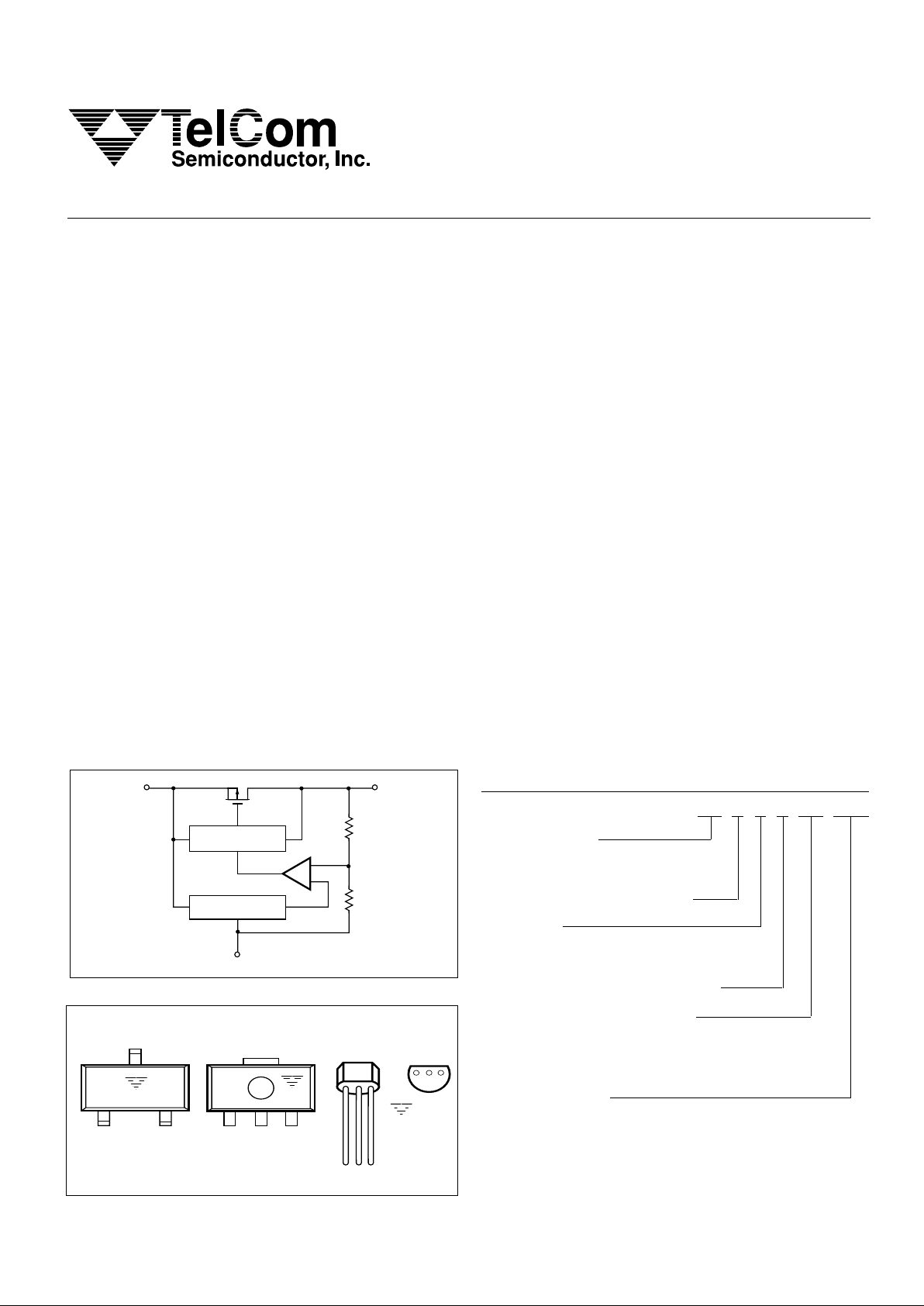
FUNCTIONAL BLOCK DIAGRAM
V
IN
V
OUT
GND
+
–
Short-circuit
Protection
Voltage
Reference
132
V
IN
V
IN
V
OUT
V
OUT
GND
GND
TC55
TC55
123
V
IN
V
OUT
GND
TC55
1
3
2
3-Pin SOT-23A
3-Pin SOT-89
3-Pin TO-92
*SOT-23A-3 is equivalent to EIAJ SC-59
PIN CONFIGURATION
Page 2
TC55 Series
2
1µA LOW DROPOUT POSITIVE VOLTAGE REGULATOR
TC55-24 9/30/99
TC55RP50 ELECTRICAL CHARACTERISTICS:
V
OUT
(S) = 5.0V, TA = 25°C unless otherwise specified (see REMARKS).
Symbol Parameter Test Conditions Min Typ Max Unit
V
OUT
(A) Output Voltage I
OUT
= 40mA — — — V
VIN = 6.0V 4.90 5.0 5.10
I
OUT
max Maximum Output Current VIN = 6.0V, V
OUT
(A) ≥ 4.5V 250 — — mA
∆V
OUT
Load Regulation VIN = 6.0 V, 1mA ≤ I
OUT
≤ 100mA — 40 80 mV
V
dif
I/O Voltage Difference I
OUT
= 100mA — 120 300 mV
I
OUT
= 200mA — 380 600
I
SS
Current Consumption VIN = 6.0V — 1.1 3.0 µA
V
OUT
(A)·100 Voltage Regulation I
OUT
= 40mA — 0.2 0.3 %/V
∆VIN·V
OUT
(S) 6.0V ≤ VIN ≤ 10.0V
V
IN
Input Voltage — — 10.0 V
∆V
OUT
(A)·10
6
Temperature Coefficient I
OUT
= 40mA — ±100 — ppm/°C
V
OUT
(S)·∆T
A
of Output Voltage – 40°C ≤ TA ≤ 85°C
Long Term Stability TA = 125°C, 1000 Hours — 0.5 — %
REMARKS:V
OUT
(S): Preset value of Output voltage
V
OUT
(A): Actual value of Output voltage
V
dif
: Definition of I/O voltage difference = {VIN1 – V
OUT
(A)}
V
OUT
(A): Output Voltage when I
OUT
is fixed and VIN = V
OUT
(S) + 1.0V
VIN1: Input Voltage when the output voltage is 98% V
OUT
(A)
TC55RP40 ELECTRICAL CHARACTERISTICS:
V
OUT
(S) = 4.0V, TA = 25°C unless otherwise specified (see REMARKS).
Symbol Parameter Test Conditions Min Typ Max Unit
V
OUT
(A) Output Voltage I
OUT
= 40mA — — — V
VIN = 5.0V 3.92 4.0 4.08
I
OUT
max Maximum Output Current VIN = 5.0V, V
OUT
(A) ≥ 3.6V 200 — — mA
∆V
OUT
Load Regulation VIN = 5.0V, 1mA ≤ I
OUT
≤ 100mA — 45 90 mV
V
dif
I/O Voltage Difference I
OUT
= 100mA — 170 330 mV
I
OUT
= 200mA — 400 630
I
SS
Current Consumption VIN = 5.0V — 1.0 2.9 µA
∆V
OUT
(A)·100 Voltage Regulation I
OUT
= 40mA — 0.2 0.3 %/V
∆VIN·V
OUT
(S) 5.0V ≤ VIN ≤ 10.0V
V
IN
Input Voltage — — 10.0 V
∆V
OUT
(A) Temperature Coefficient I
OUT
= 40mA — ±100 — ppm/°C
V
OUT
(S)·∆T
A
of Output Voltage – 40°C ≤ TA ≤ 85°C
Long Term Stability TA = 125°C, 1000 Hours — 0.5 — %
ABSOLUTE MAXIMUM RATINGS*
Item Code Ratings Units
Input Voltage V
IN
+12 V
Output Current I
OUT
Pd/(VIN – V
OUT
)mA
Output Voltage V
OUT
(VSS – 0.3) to (VIN + 0.3) V
Power Dissipation: 3-Pin SOT-23A Pd 240 mW
(TA ≤ 70°C) 3-Pin SOT-89 400
3-Pin TO-92 440
Operating Temperature Range T
A
– 40 to +85 °C
Storage Temperature Range T
stg
– 65 to +150 °C
Page 3
TC55 Series
3
1µA LOW DROPOUT POSITIVE VOLTAGE REGULATOR
TC55-24 9/30/99
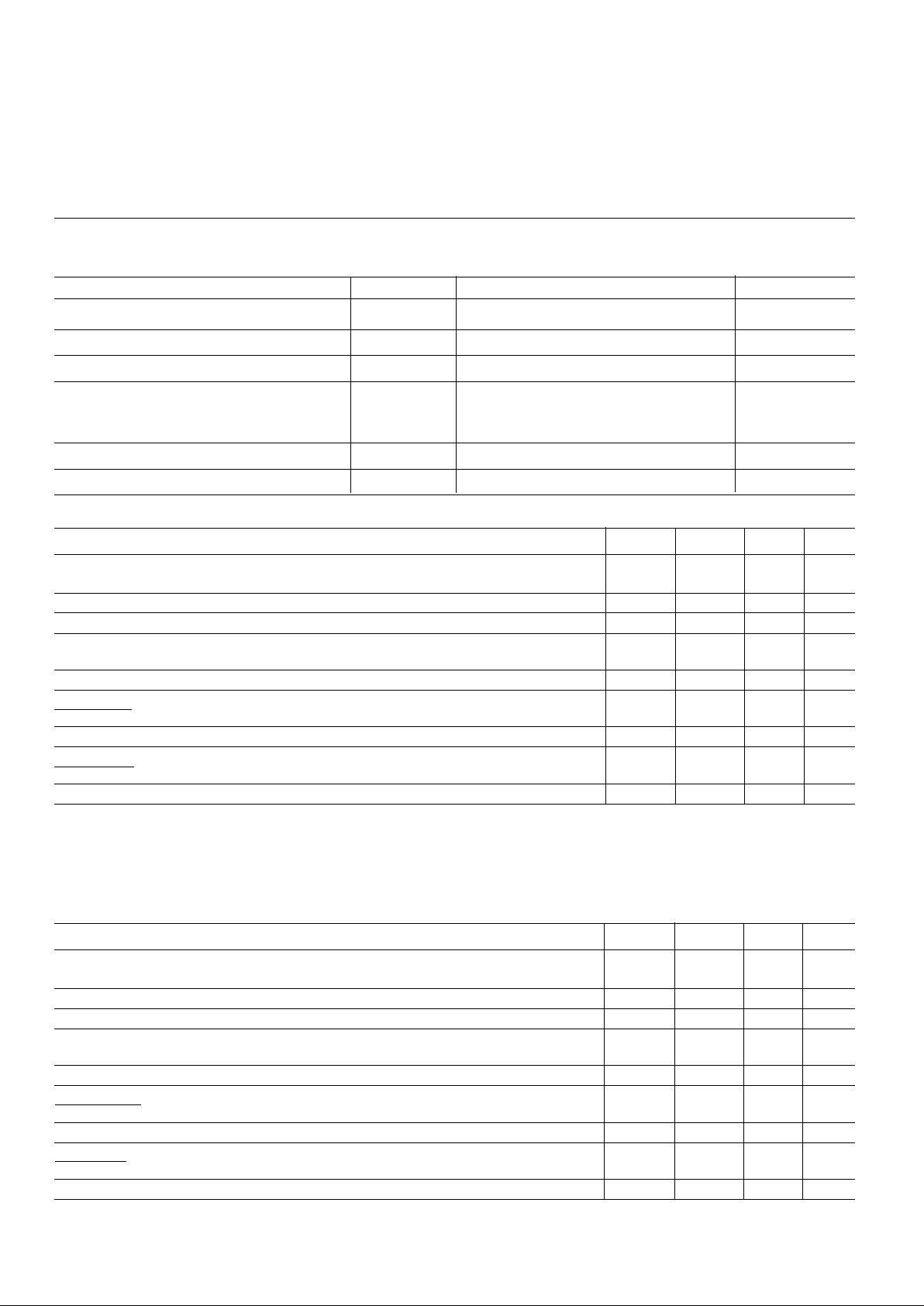
TC55RP30 ELECTRICAL CHARACTERISTICS:
V
OUT
(S) = 3.0V, TA = 25°C unless otherwise specified (see REMARKS).
Symbol Parameter Test Conditions Min Typ Max Unit
V
OUT
(A) Output Voltage I
OUT
= 40mA — — — V
VIN = 4.0V 2.94 3.0 3.06
I
OUT
max Maximum Output Current VIN = 4.0V, V
OUT
(A) ≥ 2.7V 150 — — mA
∆V
OUT
Load Regulation VIN = 4.0V, 1mA ≤ I
OUT
≤ 80mA — 45 90 mV
V
dif
I/O Voltage Difference I
OUT
= 80mA — 180 360 mV
I
OUT
= 160mA — 400 700
I
SS
Current Consumption VIN = 4.0V — 0.9 2.8 µA
V
OUT
(A)·100 Voltage Regulation I
OUT
= 40mA — 0.2 0.3 %/V
∆VIN·V
OUT
(S) 4.0V ≤ VIN ≤ 10.0V
V
IN
Input Voltage — — 10.0 V
∆V
OUT
(A)·10
6
Temperature Coefficient I
OUT
= 40mA — ±100 — ppm/°C
∆TA·V
OUT
(S) of Output Voltage – 40°C ≤ TA ≤ 85°C
Long Term Stability TA = 125°C, 1000 Hours — 0.5 — %
MARKING
3-Pin SOT-23A
3-Pin SOT-89
①
➁
➂
➃
Page 4
TC55 Series
4
1µA LOW DROPOUT POSITIVE VOLTAGE REGULATOR
TC55-24 9/30/99
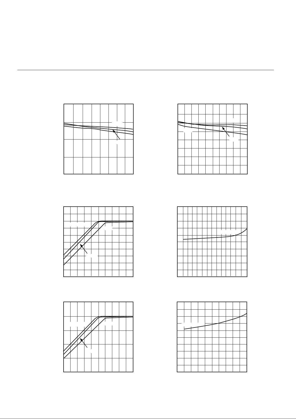
TYPICAL CHARACTERISTICS
2.9
2.8
2.7
20 40 600
160
OUTPUT CURRENT I
OUT
(mA)
OUTPUT CURRENT I
OUT
(mA)
TC55RP3002 (VIN = 4.0V)
3.0
3.1
OUTPUT VOLTAGE V
OUT
(V)
1. OUTPUT VOLTAGE vs. OUTPUT CURRENT
2. OUTPUT VOLTAGE vs. INPUT VOLTAGE
80°C
80 100 120 140
25°C
- 30°C
T
OPR
= 25°C
4.9
4.8
4.7
40 800
200160
TC55RP5002 (VIN = 6.0V)
5.0
5.1
OUTPUT VOLTAGE V
OUT
(V)
120
80°C
25°C
INPUT VOLTAGE VIN (V)
INPUT VOLTAGE VIN (V)
INPUT VOLTAGE VIN (V)
INPUT VOLTAGE VIN (V)
2.8
2.6
2.4
2.2
3.0 3.52.5
TC55RP3002
3.0
3.2
OUTPUT VOLTAGE V
OUT
(V)
OUTPUT VOLTAGE V
OUT
(V)
I
OUT
= 1mA
10mA
40mA
T
OPR
= 25°C
4.8
4.6
4.4
4.2
5.0 5.54.5
TC55RP5002
5.0
5.2
OUTPUT VOLTAGE V
OUT
(V)
I
OUT
= 1mA
10mA
40mA
T
OPR
= 25°C
5.01
5.00
4.99
4.97
4.98
4.95
4.98
67
8
9
10
5
TC55RP5002
5.03
5.02
5.04
5.05
OUTPUT VOLTAGE V
OUT
(V)
I
OUT
= 1mA
T
OPR
= 25°C
3.01
3.00
2.99
2.98
2.96
2.97
2.95
56789
1034
TC55RP3002
3.03
3.02
3.05
3.04
I
OUT
= 1mA
- 30°C
Page 5

TC55 Series
5
1µA LOW DROPOUT POSITIVE VOLTAGE REGULATOR
TC55-24 9/30/99
TYPICAL CHARACTERISTICS
0.8
0.6
0.4
0.2
0.0
–0.2
20 40
60
0
160
OUTPUT CURRENT I
OUT
(mA)
OUTPUT CURRENT I
OUT
(mA)
TC55RP3002
1.4
1.2
1.0
2.0
1.8
1.6
DROPOUT VOLTAGE V
DIF
(V)
DROPOUT VOLTAGE V
DIF
(V)
3. DROPOUT VOLTAGE vs. OUTPUT CURRENT
4. OUTPUT VOLTAGE vs. OPERATING TEMPERATURE
80 100 120 140
25°C
1.0
0.8
0.6
0.4
0.2
0.0
–0.2
40 800
200160
TC55RP5002
1.4
1.2
2.0
1.8
1.6
120
OPERATING TEMPERATURE (°C)
3.02
3.00
2.98
2.96
2.94
2.92
2.90
–40
–20 0 20 40 60 80 100
TC55RP3002 (
V
IN
= 4.0V)
3.06
3.04
3.10
3.08
OUTPUT VOLTAGE V
OUT
(V)
I
OUT
= 10mA
40mA
–30°C
–30°C
25°C
OPERATING TEMPERATURE (°C)
5.02
5.00
4.98
4.96
4.94
4.92
4.90
–40
–20 0 20 40 60 80 100
TC55RP5002 (
V
IN
= 6.0V)
5.06
5.04
5.10
5.08
OUTPUT VOLTAGE V
OUT
(V)
I
OUT
= 10mA
40mA
5. SUPPLY CURRENT vs. INPUT VOLTAGE
INPUT VOLTAGE VIN (V)
1.1
1.0
0.9
0.8
0.7
0.6
0.5
3
4567 8 910
INPUT VOLTAGE VIN (V)
5
6
78910
TC55RP3002
1.3
1.2
1.5
1.4
SUPPLY CURRENT I
SS
(µA)
1.6
1.4
1.3
1.2
1.1
1.0
0.5
1.8
1.7
2.0
1.9
SUPPLY CURRENT I
SS
(µA)
T
OPR
= 25°C
T
OPR
= 25°C
TC55RP5002
80°C
80°C
Page 6

TC55 Series
6
1µA LOW DROPOUT POSITIVE VOLTAGE REGULATOR
TC55-24 9/30/99
TYPICAL CHARACTERISTICS
0.9
0.8
0.7
0.6
0.5
–20 0
20
–40
OPERATING TEMPERATURE (°C)
TC55RP3002 (VIN = 4.0V)
1.2
1.1
1.0
1.5
1.4
1.8
6. SUPPLY CURRENT vs. OPERATING TEMPERATURE
7.INPUT TRANSIENT RESPONSE
40 60
80 100
SUPPLY CURRENT I
SS
(µA)
1.4
1.3
1.2
1.1
1.0
–20 0
20
–40
OPERATING TEMPERATURE (°C)
TC55RP5002 (VIN = 6.0V)
1.7
1.6
1.5
2.0
1.9
1.8
40 60
80 100
SUPPLY CURRENT I
SS
(µA)
TIME (msec)
7.0
6.5
6.0
5.5
5.0
5.0
4.5
4.0
–10
12
3
TC55RP5002 (
I
OUT
= 1mA)
7.5
Input
Voltage
Output
Voltage
8.0
INPUT VOLTAGE V
OUT
(V)
OUTPUT VOLTAGE V
IN
(V)
TIME (msec)
7.0
6.5
6.0
5.5
5.0
4.5
4.0
–10
12
3
TC55RP5002 (
I
OUT
= 10mA)
7.5
Input
Voltage
Output
Voltage
8.0
INPUT VOLTAGE V
OUT
(V)
OUTPUT VOLTAGE V
OUT
(V)
Page 7
TC55 Series
7
1µA LOW DROPOUT POSITIVE VOLTAGE REGULATOR
TC55-24 9/30/99
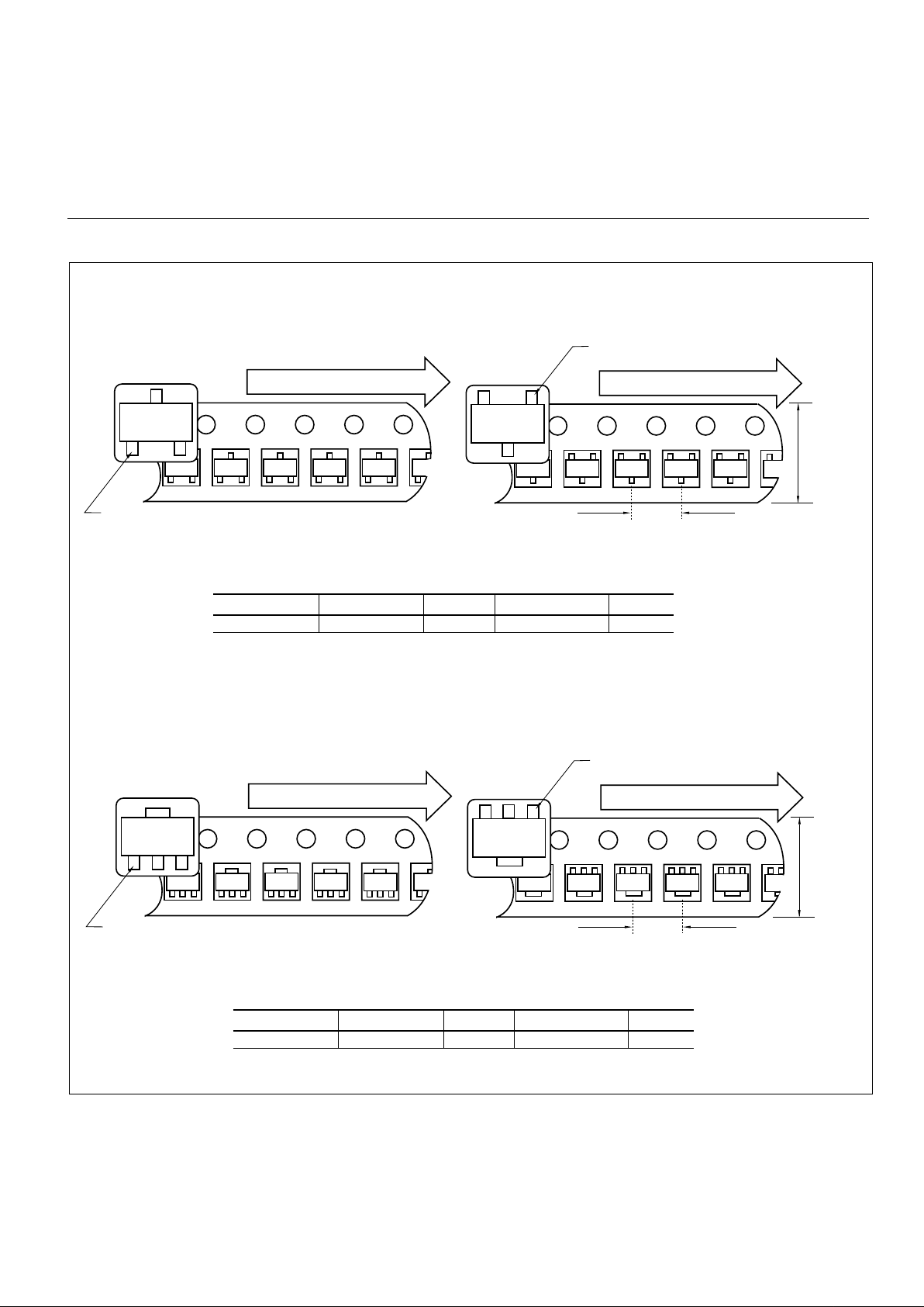
TAPING FORMS
W = Width of
Carrier Tape
User Direction of Feed
User Direction of Feed
Device
Marking
Component Taping Orientation for 3-Pin SOT-23A (EIAJ SC-59) Devices
Device
Marking
PIN 1
P = Pitch
PIN 1
Standard Reel Component Orientation
for 713 or TR Suffix Device
(Mark Right Side Up)
Reverse Reel Component Orientation
for 723 or RT Suffix Device
(Mark Upside Down)
Package Carrier Width (W) Pitch (P) Part Per Full Reel Reel Size
3-Pin SOT-23A 8 mm 4 mm 3000 7 in
Carrier Tape, Reel Size, and Number of Components Per Reel
User Direction of Feed
User Direction of Feed
Device
Marking
Component Taping Orientation for 3-Pin SOT-89 Devices
Device
Marking
PIN 1
PIN 1
Standard Reel Component Orientation
for 713 or TR Suffix Device
(Mark Right Side Up)
Reverse Reel Component Orientation
for 723 or RT Suffix Device
(Mark Upside Down)
W = Width
of Carrier
Tape
P = Pitch
Package Carrier Width (W) Pitch (P) Part Per Full Reel Reel Size
2-Pin SOT-89 12 mm 8 mm 1000 7 in
Carrier Tape, Reel Size, and Number of Components Per Reel
Page 8

TC55 Series
8
1µA LOW DROPOUT POSITIVE VOLTAGE REGULATOR
TC55-24 9/30/99
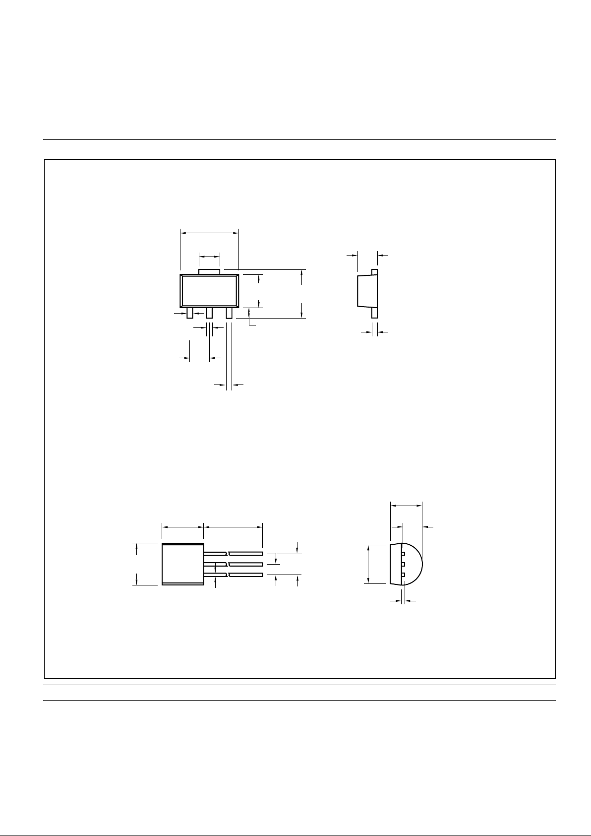
3-Pin SOT-23A (EIAJ SC-59)
.071 (1.80)
.055 (1.40)
.118 (3.00)
.098 (2.50)
.020 (0.50)
.012 (0.30)
.075 (1.90)
REFERENCE
.122 (3.10)
.106 (2.70)
.051 (1.30)
.035 (0.90)
.006 (0.15)
.000 (0.00)
.022 (0.55)
.014 (0.35)
10° MAX.
.010 (0.25)
.004 (0.09)
TAPING FORMS (Cont.)
Mark
Face
Component Taping Orientation for 3-Pin TO-92 Devices
User Direction of Feed
Seal
Tape
Back
Tape
MARK
FACE
MARK
FACE
MARK
FACE
W = Width
of Carrier
Tape
P = Pitch
Package Carrier Width (W) Pitch (P) Part Per Full Reel Reel Size
3-Pin TO-92 18 mm 12.7 mm 1000 14 in
Carrier Tape, Reel Size, and Number of Components Per Reel
PACKAGE DIMENSIONS
Dimensions: inches (mm)
Page 9
TC55 Series
9
1µA LOW DROPOUT POSITIVE VOLTAGE REGULATOR
TC55-24 9/30/99
.105 (2.67)
.095 (2.41)
.018 (0.46)
.015 (0.38)
.135
(3.43)
MIN.
.500
(12.70)
MIN.
.210 (5.33)
.170 (4.32)
.205 (5.21)
.175 (4.45)
.165 (4.19)
.125 (3.18)
.105 (2.67)
.080 (2.03)
.055 (1.40)
.045 (1.14)
.018 (0.46)
.015 (0.38)
3-Pin TO-92
Dimensions: inches (mm)
Sales Offices
TelCom Semiconductor, Inc.
1300 Terra Bella Avenue
P.O. Box 7267
Mountain View, CA 94039-7267
TEL: 650-968-9241
FAX: 650-967-1590
E-Mail: liter@telcom-semi.com
TelCom Semiconductor, GmbH
Lochhamer Strasse 13
D-82152 Martinsried
Germany
TEL: (011) 49 89 895 6500
FAX: (011) 49 89 895 6502 2
TelCom Semiconductor H.K. Ltd.
10 Sam Chuk Street, Ground Floor
San Po Kong, Kowloon
Hong Kong
TEL: (011) 852-2350-7380
FAX: (011) 852-2354-9957
.072 (1.83)
.064 (1.62)
.181 (4.60)
.173 (4.40)
.019 (0.48)
.014 (0.36)
.022 (0.56)
.017 (0.44)
.019 (0.48)
.014 (0.36)
.062 (1.60)
.056 (1.40)
.047 (1.20)
.035 (0.89)
.102 (2.60)
.090 (2.29)
.167 (4.25)
.155 (3.94)
.017 (0.44)
.014 (0.35)
.063 (1.60)
.055 (1.40)
3-Pin SOT-89
PACKAGE DIMENSIONS (CONT.)
 Loading...