

Page 1
(
)
1.5A HIGH-SPEED, FLOATING LOAD DRIVER
1
TC4403
FEATURES
■ Low Quiescent Current ......................... 300µA Max
■ Capacitive Inputs With 300mV Hysteresis
■ Both Inputs Must Be Driven to Drive Load
■ Low Output Leakage
■ High Peak Current Capability
■ Fast Output Rise Time
■ Outputs Individually Testable
APPLICATIONS
■ Isolated Load Drivers
■ Pulsers
■ Safety Interlocks
ORDERING INFORMATION
Temperature
Part No. Package Range
TC4403CPA 8-Pin PDIP 0°C to 70°C
TC4403EPA 8-Pin PDIP – 40°C to +85°C
TC4403MJA 8-Pin CerDIP – 55°C to +125°C
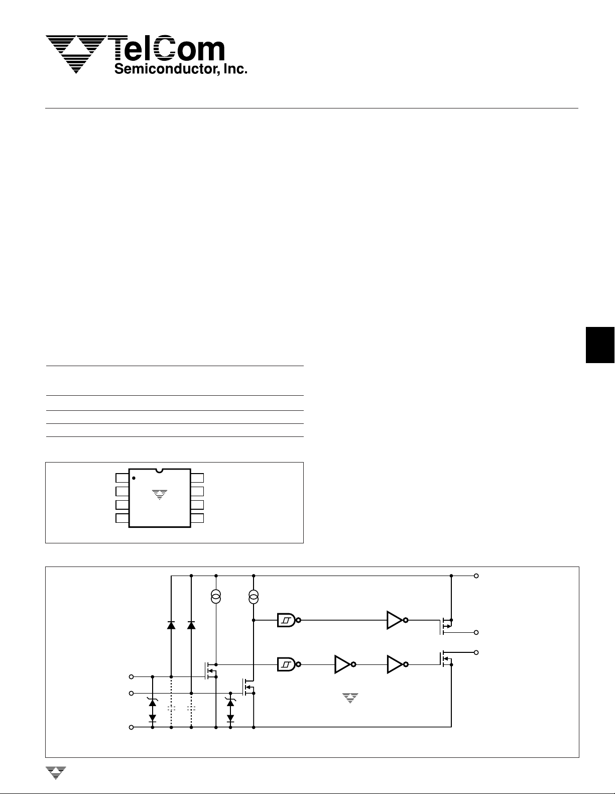
PIN CONFIGURATION
NC
IN (VDD)
GND
18
27
36
TC4403
45
NC
OUT (VDD)
V
DD
OUT (GND)IN (GND)
GENERAL DESCRIPTION
The TC4403 is a modified version of the TC4425 driver,
intended to drive floating or isolated loads requiring highcurrent pulses. The load is intended to be connected between the outputs without other reference to supply or
ground. Then, only when both logic inputs and the VDD input
are energized, is power supplied to the load. This construction allows the implementation of a wide variety of redundant
input controllers.
The low OFF-state output leakage and independence of
the two half-circuits permit a wide variety of testing schemes
to be utilized to assure functionality. The high peak current
capability, short internal delays, and fast output rise and fall
times ensure that sufficient power will be available to the
load when it is needed. The TTL and CMOS compatible
inputs allow operation from a wide variety of input devices.
The ability to swing the inputs negative without affecting
device performance allows negative biases to be placed on
the inputs for greater safety. In addition, the capacitive
nature of the inputs allows the use of series resistors on the
inputs for extra noise suppression.
The TC4403 is built for outstanding ruggedness and
reliability in harsh applications. Input voltage excursions
above the supply voltage or below ground are clamped
internally without damaging the device. The output stages
are power MOSFETs with high-speed body diodes to prevent damage to the driver from inductive kickbacks.
2
3
4
5
TOP VIEW
6
FUNCTIONAL BLOCK DIAGRAM
6
V
DD
7
5
OUT (VDD)
OUT (GND)
7
8
TC4403-6 10/11/96
4-213
300mV INPUT
HYSTERESIS
GND
4
2
3
EFFECTIVE INPUT
C = 20pF
(EACH INPUT)
TC4403
IN (GND)
IN (VDD)
TELCOM SEMICONDUCTOR, INC.
Page 2
TC4403
1.5A HIGH-SPEED,
FLOATING LOAD DRIVER
ABSOLUTE MAXIMUM RATINGS*
Supply Voltage ......................................................... +22V
Maximum Chip Temperature.................................+150°C
Storage Temperature Range ................– 65°C to +150°C
Lead Temperature (Soldering, 10 sec) .................+300°C
Package Thermal Resistance
CerDIP, R
CerDIP, R
PDIP, R
PDIP, R
Operating Temperature Range
C Version...............................................0°C to +70°C
E Version ..........................................– 40°C to +85°C
M Version .......................................– 55°C to +125°C
*Static-sensitive device. Unused devices must be stored in conductive
material. Protect devices from static discharge and static fields. Stresses
above those listed under Absolute Maximum Ratings may cause permanent damage to the device. These are stress ratings only and functional
operation of the device at these or any other conditions above those
indicated in the operational sections of the specifications is not implied.
Exposure to Absolute Maximum Rating Conditions for extended periods
may affect device reliability.
ELECTRICAL CHARACTERISTICS: T
............................................... 150°C/W
θJ-A
................................................. 50°C/W
θJ-C
.................................................. 125°C/W
θJ-A
.................................................... 42°C/W
θJ-C
A
= +25°C with 4.5V ≤ V
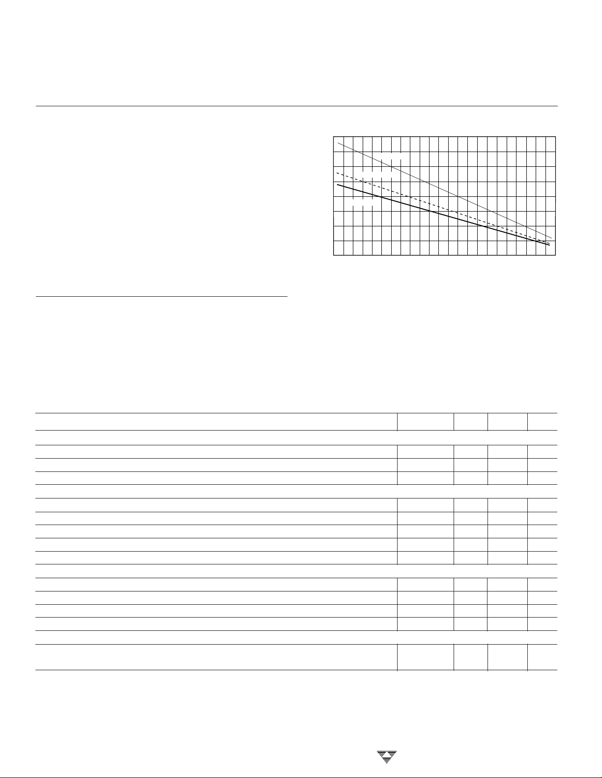
1600
1400
1200
1000
800
600
400
MAX. POWER (mW)
200
0
0
8 Pin CerDIP
8 Pin SOIC
10 20
≤ 18V, unless otherwise specified.
DD
Thermal Derating Curves
8 Pin DIP
30 40
50 60
AMBIENT TEMPERATURE (°C)
70
80 90 100 110 120
Symbol Parameter Test Conditions Min Typ Max Unit
Input
V
IH
V
IL
I
IN
Logic 1 High Input Voltage 2.4 — — V
Logic 0 Low Input Voltage — — 0.8 V
Input Current – 5V ≤ VIN ≤ V
DD
–1000 ±10 +1000 nA
Output
V
OH
V
OL
R
OS
R
OG
I
PK
High Output Voltage V
– 0.025 — — V
DD
Low Output Voltage — — 0.025 V
Sourcing Output Resistance I
Grounding Output Resistance I
= 10mA, VDD = 18V — 2.8 5 Ω
OUT
= –10mA, VDD = 18V — 3.5 5 Ω
OUT
Peak Output Current — 1.5 — A
Switching Time (Note 1)
t
R
t
F
t
D1
t
D2
Rise Time Figure 1, CL = 1800pF — 23 35 nsec
Fall Time Figure 1, CL = 1800pF — 25 35 nsec
Delay Time Figure 1, CL = 1800pF — 33 75 nsec
Delay Time Figure 1, CL = 1800pF — 38 75 nsec
Power Supply
I
S
NOTE: 1. Switching times guaranteed by design.
Power Supply Current VIN = 3V (Both Inputs) — 1.5 2.5 mA
VIN = 0V (Both Inputs) — 0.15 0.25
4-214
TELCOM SEMICONDUCTOR, INC.
Page 3

INPUT
0.1µF
MLC
1µF
WIMA
MKS-2
C = 1800pF
L
OUTPUT
10kΩ
TC4403
0.1µF
MLC
V
DD
= 16V
C = 1800pF
L
OUTPUT
10K
Ω
TC4403
t
F
+5V
INPUT
10%
90%
10%
16V
OUTPUT
t
D1
0V
t
R
+5V
INPUT
10%
90%
10%
16V
OUTPUT
t
D1
0V
0V 0V
INPUT
V
DD
= 16V
1µF
WIMA
MKS-2
1.5A HIGH-SPEED,
FLOA TING LOAD DRIVER
1
TC4403
ELECTRICAL CHARACTERISTICS: Measured over operating temperature range with 4.5V ≤ V
DD
≤ 18V
unless otherwise specified.
Symbol Parameter Test Conditions Min Typ Max Unit
Input
V
IH
V
IL
I
IN
Logic 1 High Input Voltage 2.4 — — V
Logic 0 Low Input Voltage — — 0.8 V
Input Current – 5V≤ VIN ≤ V
DD
–10,000 ±10 +10,000 nA
Output
V
OH
V
OL
R
OS
R
OG
High Output Voltage V
Low Output Voltage — — 0.025 V
Sourcing Output VIN = 2.4V — 3.7 8 Ω
Resistance I
Grounding Output VIN = 2.4V — 4.3 8 Ω
Resistance I
= 10mA, VDD = 18V
OUT
= –10mA, VDD = 18V
OUT
– 0.025 — — V
DD
Switching Time (Note 1)
t
R
t
F
t
D1
t
D2
Rise Time Figure 1, CL = 1800pF — 28 60 nsec
Fall Time Figure 1, CL = 1800pF — 32 60 nsec
Delay Time Figure 1, CL = 1800pF — 32 100 nsec
Delay Time Figure 1, CL = 1800pF — 38 100 nsec
Power Supply
I
S
Power Supply Current VIN = 3V (Both Inputs) — 2 3.5 mA
VIN = 0V (Both Inputs) — 0.2 0.3
2
3
4
NOTE: 1. Switching times guaranteed by design.
Figure 1. Switching Time Test Circuits
TELCOM SEMICONDUCTOR, INC.
5
6
7
8
4-215
Page 4

TC4403
t (nsec)
4681012
14 16 18
Fall Time vs. Supply Voltage
FALL
100
80
60
40
20
0
V
DD
1000pF
1500pF
TA = +25°C
4700pF
3300pF
2200pF
470pF
TYPICAL CHARACTERISTICS
Rise Time vs. Supply Voltage
100
4700pF
80
3300pF
60
2200pF
40
RISE
t (nsec)
20
470pF
0
4681012
V
DD
1.5A HIGH-SPEED,
FLOATING LOAD DRIVER
TA = +25°C
1500pF
1000pF
14 16 18
t (nsec)
4-216
TIME (nsec)
Rise Time vs. Capacitive Load
100
TA = +25°C
80
60
40
RISE
20
0
100 1000
C (pF)
LOAD
Rise and Fall Times vs.
Temperature
32
C = 2200pF
30
28
26
24
22
20
18
LOAD
V
= 18V
DD
t
RISE
t
FALL
–55 –35 5 25 45 65 85 105 125–15
TEMPERATURE (°C)
t
FALL
t
RISE
5V
10V
15V
10,000
Fall Time vs. Capacitive Load
100
TA = +25°C
80
60
FALL
40
t (nsec)
20
0
100 1000 10,000
C (pF)
LOAD
Propagation Delay vs.
Input Amplitude
C = 2200pF
100
t
D1
80
60
40
DELAY TIME (nsec)
20
0123456789101112
INPUT (V)
LOAD
V = 10V
DD
t
TELCOM SEMICONDUCTOR, INC.
5V
10V
15V
D2
Page 5

1.5A HIGH-SPEED,
FLOA TING LOAD DRIVER
TYPICAL CHARACTERISTICS (Cont.)
1
TC4403
Delay Time vs. Supply Voltage
50
45
40
35
30
DELAY TIME (nsec)
25
20
4 6 8 1012141618
C = 2200pF
LOAD
TA = +25°C
t
D2
t
D1
V
DD
Quiescent Current vs. Voltage
T = +25°C
A
1
0.1
QUIESCENT
I (mA)
BOTH INPUTS = 1
BOTH INPUTS = 0
Delay Time vs. Temperature
50
C = 2200pF
LOAD
45
40
35
30
DELAY TIME (ns)
25
20
–55 –35 –15 5 25 45 65 85 105 125
TEMPERATURE (°C)
t
D2
t
D1
Quiescent Current vs. Temperature
1.4
1.2
1.0
0.8
0.6
QUIESCENT
I (mA)
0.4
INPUTS = 1
2
3
4
5
0.01
4 6 8 1012141618
V
DD
Typical Discharge Characteristics
5.7
5.1
4.5
3.9
3.3
2.7
CLOSED CIRCUIT VOLTAGE
2.1
1.5
0
75 150 225 300
HOURS OF SERVICE
2.768V
+
+
75 HOURS
2.727V
525
0.2
0.0
–55 –35 –15 5 25 45 65 85 105 125
INPUTS = 0
TEMPERATURE (°C)
TYPICAL APPLICATION
+15V
POWER
R
FIRE
ARM
T
R
T
1 MΩ
–15V
TC4422
2
4
1 MΩ
6
6
TC4403
3
3
6
7
R
LOAD
5
7
8
TELCOM SEMICONDUCTOR, INC.
4-217
 Loading...