

Page 1
M
TC429
6A Single High-Speed, CMOS Power MOSFET Driver
Features
• High Peak Output Current: 6A
• Wide Operating Range: 7V to 18V
• High Impedance CMOS Logic Input
• Logic Input Threshold Independent of Supply
Voltage
• Low Supply Current
- With Logic 1 Input – 5mA Max
- With Logic 0 Input – 0.5mA Max
• Output Voltage Swing Within 25mV of Ground
or V
DD
• Short Delay Time: 75nsec Max
• High Capacitive Load Drive Capability
-t
, t
RISE
C
LOAD
= 35nsec Max With
FALL
= 2500pF
Applications
• Switch-Mode Power Supp lie s
• CCD Drivers
• Pulse Transformer Drive
• Class D Switching Amplifiers
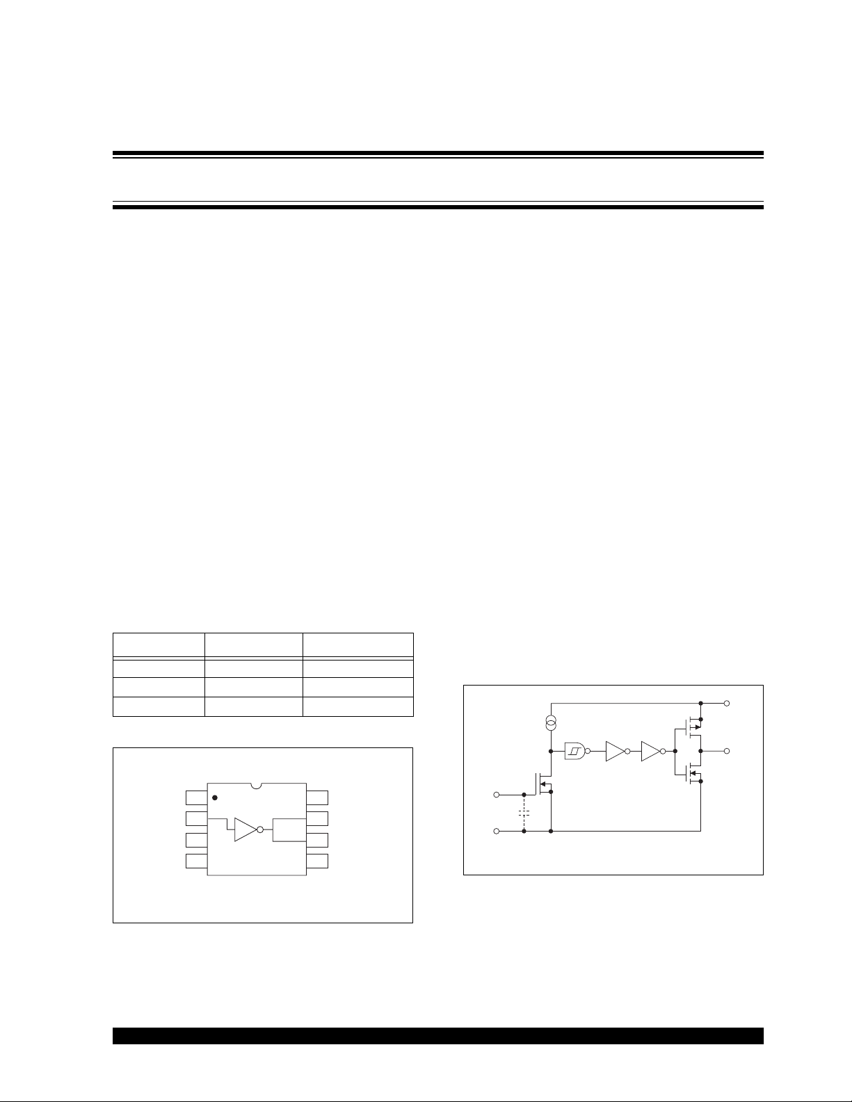
Device Selection Table
Part Number Package Temp. Range
TC429CPA 8-Pin PDIP 0°C to +70°C
TC429EPA 8-Pin PDIP -40°C to +85°C
TC429MJA 8-Pin CERDIP -55°C to +125°C
General Description
The TC429 is a high-speed, single CMOS-level
translator and driver. Designed specifically to drive
highly capacitive power MOSFET gates, the TC429
features 2.5Ω output impedance and 6A peak output
current drive.
A 2500pF capaciti ve load will be drive n 1 8V i n 2 5ns ec .
The rapid switching times with large capacitive loads
minimize MOSFET transition power loss.
A TTL/CMOS input logic level is translated into an
output voltage swing that equals the supply and will
swing to with in 25mV of gr ound or V
swing may equal the supply. Logic input current is
under 10µA, making direct interface to CMOS/bipolar
switch-mode power supply controllers easy. Input
“speed-up” capacitors are not required.
The CMOS design minimizes quiescent power supply
current. With a logic 1 input, power supply current is
5mA maximum and decreases to 0.5mA for logic 0
inputs.
For dual devices, see the TC426/TC427/TC428,
TC4426/TC4427/TC4428 and TC4426A/TC4427A/
TC4428A data sheets.
For noninverting applications, or applications requiring
latch-up protection, see the TC4420/TC4429 data
sheet.
. Input voltage
DD
Typical Application
1,8
V
DD
Package Type
8-Pin PDIP/CERDIP
2
V
18
DD
27
INPUT
NC
36
45
NC = No internal connection
NOTE: Duplicate pins must both be connected for proper operation.
2002 Microchip Technology Inc. DS21416B-page 1
TC429
V
DD
OUTPUT
OUTPUT
GNDGND
Input
GND
4,5
Effective
Input
C = 38pF
300mV
TC429
6,7
Output
Page 2
TC429
1.0 ELECTRICAL
CHARACTERISTICS
Absolute Maximum Ratings*
Supply Voltage.....................................................+20V
*Stresses above those listed under "Absolute Maximum
Ratings" may cause permanent damage to the device. These
are stress ratings only and functional operation of the device
at these or any other conditions above those indicated in the
operation sections of the specifications is not implied.
Exposure to Absolute Maximum Rating conditions for
extended periods may affect device reliability.
Input Voltage, Any Terminal
...................................V
+ 0.3V to GND – 0.3V
DD
Power Dissipation (TA ≤ 70°C)
PDIP.........................................................730mW
CERDIP....................................................800mW
Derating Factor
PDIP.................................5.6mW/°C Above 36°C
CERDIP................................................6.4mW/°C
Operating Temperature Range
C Version.........................................0°C to +70°C
E Version......................................-40°C to +85°C
M Ve rsion ...................................-55°C to +125°C
Storage Temperature Range..............-65°C to +150°C
TC429 ELECTRICAL SPECIFICATIONS
Electrical Characteristics: TA = +25°C with 7V ≤ V
Symbol Parameter Min Typ Max Units Test Conditions
Input
V
IH
V
IL
I
IN
Output
V
OH
V
OL
R
O
I
PK
Switching Time (Note 1)
t
R
t
F
t
D1
t
D2
Power Supply
I
S
Note 1: Switching times ensured by design.
Logic 1, High Input Voltage 2.4 1.8 — V
Logic 0, Low Input Voltage — 1.3 0.8 V
Input Curre n t -10 — 10 µA0V ≤ V
High Output Voltage VDD – 0.025 —— V
Low Output Voltage ——0.025 V
Output Resistance — 1.8 2.5 Ω VIN = 0.8V,
Peak Output Current — 6 — AVDD = 18V (Figure 3-4)
Rise Time — 23 35 nsec Figure 3-1, CL = 2500pF
Fall Time — 25 35 nsec Figure 3-1, CL = 2500pF
Delay Time — 53 75 nsec Figure 3-1
Delay Time — 60 75 nsec Figure 3-1
Power Supply Current —
≤ 18V, unless otherwise noted.
DD
— 1.5 2.5
3.5
—
0.3
0.5
≤ V
IN
DD
= 10mA, VDD = 18V
I
OUT
Ω V
5
mA VIN = 3V
= 2.4V,
IN
I
= 10mA, VDD = 18V
OUT
V
= 0V
IN
DS21416B-page 2 2002 Microchip Technology Inc.
Page 3
TC429
TC429 ELECTRICAL SPECIFICATIONS (CONTINUED)
Electrical Characteristics: Over operating temperature range with 7V ≤ V
Symbol Parameter Min Typ Max Units Test Conditions
Input
V
IH
V
IL
I
IN
Logic 1, High Input Voltage 2.4 —— V
Logic 0, Low Input Voltage ——0.8 V
Input Current -10 — 10 µA0V ≤ V
Output
V
OH
V
OL
R
O
High Output Voltage VDD – 0.025 ——V
Low Output Voltage ——0.025 V
Output Resistance ——5 Ω VIN = 0.8V,
——5
Switching Ti me (Note 1)
t
R
t
F
t
D1
t
D2
Rise Time ——70 nsec Figure 3-1, CL = 2500pF
Fall Time ——70 nsec Figure 3-1, CL = 2500pF
Delay Time ——100 nsec Figure 3-1
Delay Time ——120 nsec Figure 3-1
Power Supply
I
S
Note 1: Switching times ensured by design.
Power Supply Current —
—
—
—
≤ 18V, unless otherwise noted.
DD
I
OUT
12
Ω V
mA VIN = 3V
1
I
OUT
V
IN
IN
≤ V
IN
DD
= 10mA, VDD = 18V
= 2.4V,
= 10mA, VDD = 18V
= 0V
2002 Microchip Technology Inc. DS21416B-page 3
Page 4

TC429
2.0 PIN DESCRIPTIONS
The descriptions of the pins are listed in Table 2-1.
TABLE 2-1: PIN FUNCTION TABLE
Pin No.
(8-Pin PDIP,
CERDIP)
1V
2 INPUT Control input, TTL/CMOS compatible logic input.
3 NC No connection.
4 GND Ground.
5 GND Ground.
6 OUTPUT CMOS totem-pole output, common to Pin 7.
7 OUTPUT CMOS totem-pole output, common to Pin 6.
8V
Symbol Description
DD
DD
Supply input, 7V to 18V.
Supply input, 7V to 18V.
DS21416B-page 4 2002 Microchip Technology Inc.
Page 5
TC429
3.0 APPLICATIONS INFORMATION
3.1 Supply Bypassing
Charging and discharging large capacitive loads
quickly re qui res la rge cur rents . F or exam ple , ch argi ng
a 2500pF load to 18 V in 25nsec requires a 1.8A current
from the device’s power supply.
T o ensu re low supply im pedance over a wide frequency
range, a parallel capacitor combination is recommended for supply bypas sing. Low-induc tance ceramic
disk capacitors w ith short lead lengt hs (< 0.5 in.) shoul d
be used. A 1µF film c apac itor in p aral lel with o ne or tw o
0.1µF ceramic disk capacitors normally provides
adequate bypassing.
3.2 Grounding
The high-current capability of the TC429 demands
careful PC board layout for best performance. Since
the TC429 is an inverting driver, any ground lead
impedance will ap pear as negati ve feedback which can
degrade switching speed. The feedback is especially
noticeable with slow rise-time inputs, such as those
produced by an open-col lector outp ut with resis tor pullup. The TC429 input s tructure includes about 300mV of
hysteresis to ensure clean transitions and freedom
from oscillation, but attention to layout is still
recommended.
Figure 3-3 shows the feedback effect in detail. As the
TC429 input begins to go positive, the output goes
negative and several amperes of current flow in the
ground le ad. As l ittle as 0.05 Ω of PC trac e resistance
can produce hundre ds of millivolt s at the TC429 gro und
pins. If the driving logic is referenced to power ground,
the effective logi c input level is reduce d and oscillations
may result.
To ensure optimum device performance, separate
ground traces should be provided for the logic and
power connections. Con necting log ic ground di rectly to
the TC429 GND pins e nsures full logic d rive to the input
and fast output switching. Both GND pins should be
connected to power ground.
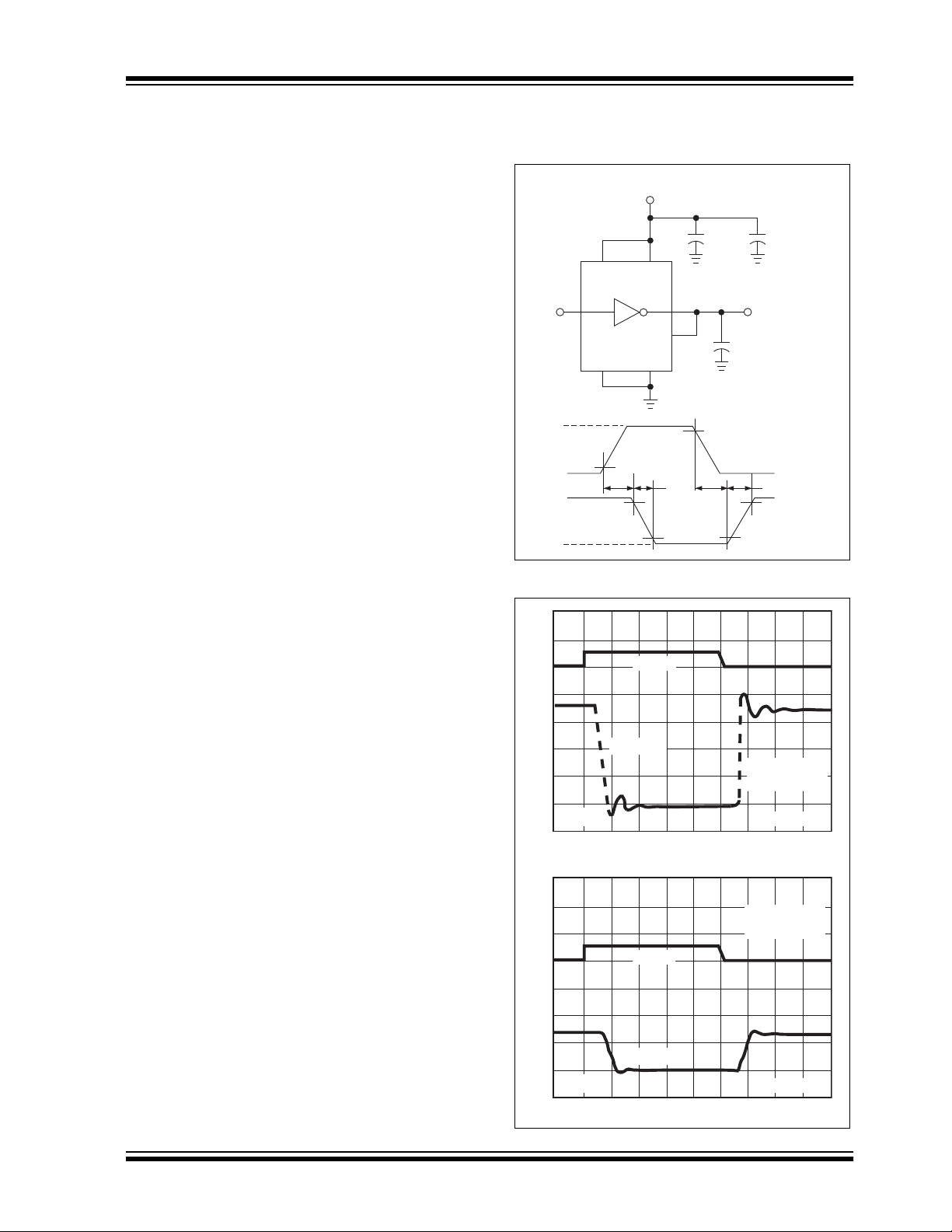
FIGURE 3-1: INVERTING DRIVER
SWITCHING TIME
TEST CIRCUIT
= 18V
V
DD
Output
CL = 2500pF
Input: 100kHz,
square wave,
t
= t
RISE
FALL
t
R
10%10%
0.1µF
18
26
Input
7
TC429
45
+5V
Input
10%
0V
18V
Output
0V
t
D1
90% 90%
t
F
t
1µF
90%
D2
FIGURE 3-2: SWITCHING SPEED
INPUT
OUTPUT
VOLTAGE (5V/DIV)
5V
TIME (100ns/DIV)
CL = 2500pF
V
= 18V
S
100ns
≤ 10nsec
CL = 2500pF
V
= 7V
S
INPUT
VOLTAGE (5V/DIV)
OUTPUT
5V
TIME (100ns/DIV)
2002 Microchip Technology Inc. DS21416B-page 5
100ns
Page 6

TC429
FIGURE 3-3: SWITCHING TIME
DEGRADATION DUE TO
NEGATIVE FEEDBACK
+18V
TC429
2.4V
0V
Logic
Ground
Power
Ground
300 mV
1
8
2
5
4
1µF
TEK Current
Probe 6302
6,7
0.1µF0.1µF
6A
PC Trace Resistance = 0.05W
18V
0V
2500pF
3.3 Input St age
The input voltage level changes the no-load or
quiescent supply current. The N-channel MOSFET
input stage transi stor drives a 3mA current sourc e load.
With a logic “1” input, the maximum quiescent supply
current is 5mA. Logic “0” input level signals reduce
quiescent current to 500µA maximum.
The TC429 input is designed to provide 300mV of
hysteresis, providing clean transitions and minimizing
output stage current spiking when changing states.
Input voltage level s are approximately 1 .5V , maki ng the
device TTL compatible over the 7V to 18V operating
supply range. Input current is less than 10µA over this
range.
The TC429 can be directly driven by TL494, SG1526/
1527, SG1524, SE5560 or similar switch-mode
power supply integrated circuits. By off-loading the
power-dri ving duties to t he TC429, the power supply
controller can operate at lower dissipation, improving
performance and reliability.
FIGURE 3-4: PEAK OUTPUT CURRENT
TEST CIRCUIT
+18V
1µF
18V
0V
2500pF
0V
2.4V
6,7
TEK Current
Probe 6302
0.1µF0.1µF
1
8
2
5
4
TC429
3.4 Power Dissipation
CMOS circuits usually permit the user to ignore power
dissipation. Logic families such as the 4000 and 74C
have outputs th at can only s upply a few milliamperes of
current, an d even shorting outputs to gro und will not
force enough current to destroy the dev ice. The TC429,
however , can source or sink seve ral ampere s and driv e
large capacitive loads at high frequency. The package
power dissipation limit can easily be exceeded.
Therefore, some attention should be given to power
dissipation when driving low impedance loads and/or
operating at high frequency.
The supply current versus frequency and supply
current versus cap acitive lo ad charac teristic curv es will
aid in determining power dissipation calculations.
Table 3-1 lists the maximum operating frequency for
several power supply voltages when driving a 2500pF
load. More accurate power dissipation figures can be
obtained by summing the three power sources.
Input signal duty cycle, power supply voltage and
capacitive load influence package power dissipation.
Given power dissipation and package thermal resistance, the maximum ambient operation temperature
is easily calculated. The 8-pin CERDIP junction-toambient thermal resistance is 150°C/W. At +25°C, the
package is rated at 800mW maximum dissipation.
Maximum allowable chip temperature is +150°C.
DS21416B-page 6 2002 Microchip Technology Inc.
Page 7

TC429
Three components make up total package power
dissipation:
• Capacitive load dissipation (P
)
C
• Quiescent power (PQ)
• Transition power (P
)
T
The capacitive l oad-ca used d issip ati on is a direct function of frequency, capacitive load and supply voltage.
The package power dissipation is:
= f C V
P
C
2
S
Where:
f = Switching frequency
C = Capacitive load
V
= Supply voltage
S
Quiescent power dissipation depends on input signal
duty cycle. A logic low input results in a low-power
dissipation mode with only 0.5mA total current drain.
Logic high signals raise the current to 5mA maximum.
The quiescent power dissipation is:
= VS (D (IH) + (1 – D) IL)
P
Q
Where:
= Quiescent current with input high (5mA max)
I
H
I
= Quiescent current with input low
L
(0.5mA max)
D = Duty cycle
Transitio n po wer dis si p ation arises because the outp ut
stage N- and P-channel MOS transistors are ON
simultaneously for a very short period when the output
changes.
The transition package power dissipation is
approximately:
= f VS (3.3 x 10⁻⁹ A • Sec)
P
T
An example shows the relative magnitude for each
item.
C = 2500pF
VS= 15V
D = 50%
f = 200kHz
P
= Package power dissipation = PC + PT + P
D
= 113mW + 10mW + 41mW
= 164mW
Maximum operating temperature = T
– θJA (PD)
J
= 125°C
Where:
= Maximum allowable junction temperature
T
J
(+150°C)
θ
= Junction-to-ambient therm al resi stance
JA
(150°C/W, CERDIP)
Note: Ambient operating temperature should not
exceed +85°C for I JA devices or +125°C for
MJA devices.
T ABLE 3-1: MAXIMUM OPERATING
FREQUENCIES
V
S
18V 500kHz
15V 700kHz
10V 1.3MHz
5V >2MHz
CONDITIONS: 1. CERDIP Package (θJA =150°C/W)
2. T
3. C
= +25°C
A
= 2500pF
L
f
MAX
FIGURE 3-5: PEAK OUTPUT
CURRENT CAPABILITY
5V/DIV
500mV/DIV
(5 AMP/DIV)
5V
INPUT
OUTPUT
500mV
TIME (5µs/DIV)
VS = 18V
R
= 0.1Ω
L
5µs
3.5 POWER-ON OSCILLATION
Note: It is extremely important that all MOSFET
Q
Power-on oscillations are due to trace size and layout
as well as component placement. A ‘quick fix’ for most
applications which exhibit power-on oscillation
problems is to plac e a ppro xi ma tely 10 kΩ in series wi th
the input of the MOSFET driver.
Driver applications be evaluated for
the possibility of having High-Power
Oscillations occurring during the power-on
cycle.
2002 Microchip Technology Inc. DS21416B-page 7
Page 8

TC429
60
50
0
30
0
0
5101520
)
(
)
ge
C
L
60
50
0
30
0
0
0
5
)
e
525
50100125150
t
t
R
t
t
00
0
00
0K
)
(
)
d
t
t
90
80
0
60
50
0
075
)
(
)
e
525
50100125
t
t
0
60
50
0
30
0
0
0
(
)
010010K
)
00kHz
0kHz
d
T
C
z
0
0
00
80
60
0
5
(
)
ge
01520
)
t
t
C
C
pF
5V
50
50
0
30
0
0
0
0100
1
15V
0V
8V
5V
T
C
C
(
)
)
y
4
0816
20
ge
(
)
)
4
3
5-25
50100
50
e
(
)
C)
50
02575125
5
C
8
C
4.0 TYPICAL CHARACTERISTICS
Note: The graphs and tables provided following this note are a statistical summary based on a limited number of
samples and are pro vided for information al purposes only. The performance characte ristics listed herei n are
not tested or guaranteed. In some graphs or tables, the data presented may be outside the specified
operating range (e.g., outside specified power supply range) and therefore outside the warranted range.
Rise/Fall Times vs. Supply Volta
4
nsec
IME
2
1
SUPPLY VOLTAGE (V
Supply Current vs. Capacitive Loa
7
mA
4
400kH
2
UPPLY CURRENT
1
1
2
2
CAPACITIVE LOAD (pF
Rise/Fall Times vs. Temperatur
4
2
1
-50-2
7
C
Delay Times vs. Temperatur
= +1
nsec
7
DELAY TIME
4
-50-2
C
Rise/Fall Times vs. Capacitive Loa
1
nsec
1
IME
1
CAPACITIVE LOAD (pF
Delay Times vs. Supply Volta
14
= 2500
4
1
SUPPLY VOLTAGE (V
1
12
nsec
1
ELAY TIME
1
Supply Current vs. Frequenc
4
mA
2
UPPLY CURRENT
1
FREQUENCY (kHz
1
= 1
1
Supply Current vs. Supply Volta
= +2
=
mA
UPPLY CURRENT
SUPPLY VOLTAGE (V
Supply Current vs. Temperatur
= +1
=
mA
UPPLY CURRENT
-7
-
1
DS21416B-page 8 2002 Microchip Technology Inc.
Page 9

TYPICAL CHARACTERISTICS (CONTINUED)
S
310mV
V
3
300mV
5
0
5
5
C
(
)
300
00
00
)
06080100
5V
0V
15V
15V
18V
18V
5
C
Hig
t
(
)
00
300
00
00
)
020406080100
5V
0V
15V
18V
5
t
00
00
000
00
00
600
04070100110120
)
P
TC429
Voltage Transfer Characteristics
20
TA = +2
°
1
V
1
UTPUT VOLTAGE
0
0.25 0.50 0.75 1 1.50 1.75 2
INPUT VOLTAGE (V)
1
14
12
1
MAX. POWER (mW)
4
2
Pin CERDIP
HYSTERESI
200m
1.25
Thermal Derating Curves
-Pin DI
h Output Voltage vs. Curren
400
= +2
2
1
UTPUT VOLTAGE (mV)
0204
CURRENT SOURCED (mA
Low Output Voltage vs. Curren
4
= +2
=
1
mV
2
1
UTPUT VOLTAGE
CURRENT SUNK (mA
=
1
102
AMBIENT TEMPERATURE (C
2002 Microchip Technology Inc. DS21416B-page 9
Page 10

TC429
)
)
)
)
)
)
)
)
)
)
)
)
)
)
)
)
)
)
)
)
)
)
)
)
P
)
)
)
)
)
)
.
.
)
)
)
)
)
)
)
)
)
)
)
)
)
)
)
)
)
5.0 PACKAGING INFORMATION
5.1 Package Marking Information
Package mar k ing data not avai lable at this ti me.
5.2 Package Dimensions
-Pin Plastic DI
.260 (6.60
.240 (6.10
.045 (1.14
.030 (0.76
.400 (10.16
.348 (8.84
.200 (5.08
.140 (3.56
.150 (3.81
.115 (2.92
.110 (2.79
.090 (2.29
8-Pin CERDIP (Narrow)
.110 (2.79
.090 (2.29
.070 (1.78
.040 (1.02
.022 (0.56
.015 (0.38
.040 (1.02
.020 (0.51
.300 (7.62
.230 (5.84
.310 (7.87
.290 (7.37
.015 (0.38
.008 (0.20
.400 (10.16
.310 (7.87
Dimensions: inches (mm)
.055 (1.40) MAX
.200 (5.08
.160 (4.06
.200 (5.08
.125 (3.18
.400 (10.16
.370 (9.40
.065 (1.65
.045 (1.14
.020 (0.51
.016 (0.41
.020 (0.51) MIN
.040 (1.02
.020 (0.51
.150 (3.81
.015 (0.38
.008 (0.20
.320 (8.13
.290 (7.37
.400 (10.16
.320 (8.13
Dimensions: inches (mm)
DS21416B-page 10 2002 Microchip Technology Inc.
Page 11

TC429
Sales and Support
Data Sheets
Products supported by a preliminary Data Sheet may have an errata sheet describing minor operational differences and recommended workarounds. To determine if an errata sheet exists for a particular device, please contact one of the following:
1. Your local Microchip sales office
2. The Microchip Corporate Literature Center U.S. FAX: (480) 792-7277
3. The Microchip Worldwide Site (www.microchip.com)
Please specify which device, revision of silicon and Data Sheet (include Literature #) you are using.
New Customer Notification System
Register on our web site (www.microchip.com/cn) to receive the most current information on our products.
2002 Microchip Technology Inc. DS21416B-page11
Page 12

TC429
NOTES:
DS21416B-page12 2002 Microchip Technology Inc.
Page 13

TC429
Information contained in this publication regarding device
applications and the like is intended through suggestion only
and may be superseded by updates. It is your responsibility to
ensure that your application meets with your specifications.
No representation or warranty is given and no liability is
assumed by Microchip Technology Incorporated with respect
to the accuracy or use of such information, or infringement of
patents or other intellectual property rights arising from such
use or otherwise. Use of Microchip’s products as critical components in life support systems is not authorized except with
express written approval by Microchip. No licenses are conveyed, implicitly or otherwise, under any intellectual property
rights.
Trademarks
The Microchip name and logo, the Microchip logo, FilterLab,
EELOQ, microID, MPLAB, PIC, PICmicro, PICMASTER,
K
PICSTART, PRO MATE, SEEVAL and The Embedded Co ntrol
Solutions Company are registered trademarks of Microchip Technology Incorporated in the U.S.A. and other countries.
dsPIC, ECONOMONITOR, FanSense, FlexROM, fuzzyLAB,
In-Circuit Serial Programming, ICSP, ICEPIC, microPort,
Migratable Memory, MPASM, MPLIB, MPLINK, MPSIM,
MXDEV, PIC C, PICDEM, PICDEM.net, rfPIC, Select Mode
and T otal Endurance are trademarks of Microchip T echnology
Incorporated in the U.S.A.
Serialized Quick Turn Programming (SQTP) is a service mark
of Microchip Technology Incorpora ted in the U.S.A.
All other trademarks mentioned herein are property of their
respective companies.
© 2002, Microchip Technology Incorporated, Printed in the
U.S.A., All Rights Reserved.
Printed on recycled paper.
Microchip received QS-9000 quality system
certification for its worldwide headquarters,
design and wafer fabrication facilities in
Chandler and Tempe, Arizona in July 1999
and Mountain View, California in March 2002.
The Company’s quality system processes and
procedures are QS-9000 compliant for its
PICmicro
devices, Serial EEPROMs, micrope ri ph era ls,
non-volatile memory and ana l og pro duc ts. In
addition, Microchip’s quality system for the
design and manufacture of development
systems is ISO 9001 certified.
®
8-bit MCUs, KEELOQ
®
code hoppin g
2002 Microchip Technology Inc. DS21416B-page 13
Page 14

M
WORLDWIDE SALES AND SERVICE
AMERICAS
Corporate Office
2355 West Chandler Blvd.
Chandler, AZ 85224-6199
Tel: 480-792-7200 Fax: 480-792-7277
Technical Support: 480-792-7627
Web Address: http://www.microchip.com
Rocky Mountain
2355 West Chandler Blvd.
Chandler, AZ 85224-6199
Tel: 480-792-7966 Fax: 480-792-7456
Atlanta
500 Sugar Mill Road, Suite 200B
Atlanta, GA 30350
Tel: 770-640-0034 Fax: 770- 640 -03 07
Boston
2 Lan Drive, Suite 120
Westford, MA 01886
Tel: 978-692-3848 Fax: 978- 692 -38 21
Chicago
333 Pierce Road, Suite 180
Itasca, IL 60143
Tel: 630-285-0071 Fax: 630-285-0075
Dallas
4570 Westgrove Drive, Suite 160
Addison, TX 75001
Tel: 972-818-7423 Fax: 972- 818 -29 24
Detroit
Tri-Atria Office Building
32255 Northwestern Highway, Suite 190
Farmington Hills, MI 48334
Tel: 248-538-2250 Fax: 248-538-2260
Kokomo
2767 S. Albright Road
Kokomo, Indiana 46902
Tel: 765-864-8360 Fax: 765-864-8387
Los Angeles
18201 Von Karman, Suite 1090
Irvine, CA 92612
Tel: 949-263-1888 Fax: 949- 263 -13 38
New York
150 Motor Parkway, Suite 202
Hauppauge, NY 11788
Tel: 631-273-5305 Fax: 631- 273 -53 35
San Jose
Microchip Technology Inc.
2107 North First Street, Suite 590
San Jose, CA 95131
Tel: 408-436-7950 Fax: 408- 436 -79 55
Toronto
6285 Northam Drive, Suite 108
Mississauga, Ontario L4V 1X5, Cana da
Tel: 905-673-0699 Fax: 905-673-6509
ASIA/PACIFIC
Australia
Microchip Technology Australia Pty Ltd
Suite 22, 41 Rawson Street
Epping 2121, NSW
Australia
Tel: 61-2-9868-6733 Fax: 61-2-9868-6755
China - Beij ing
Microchip Technology Consulting (Shanghai)
Co., Ltd., Beijing Liaison Office
Unit 915
Bei Hai Wan Tai Bldg.
No. 6 Chaoyangmen Beidajie
Beijing, 100027, No. China
Tel: 86-10-85282100 Fax: 86-10-85282104
China - Chengdu
Microchip Technology Consulting (Shanghai)
Co., Ltd., Chengdu Liaison Office
Rm. 2401, 24th Floor,
Ming Xing Financial Tower
No. 88 TIDU Street
Chengdu 610016, China
Tel: 86-28-6766200 Fax: 86-28-6766599
China - Fuzhou
Microchip Technology Consulting (Shanghai)
Co., Ltd., Fuzhou Liaison Of fice
Unit 28F, World Trade Plaza
No. 71 Wusi Road
Fuzhou 350001, China
Tel: 86-591-7503506 Fax: 86-591-7503521
China - Shanghai
Microchip Technology Consulting (Shanghai)
Co., Ltd.
Room 701, Bldg. B
Far East International Plaza
No. 317 Xian Xia Road
Shanghai, 200051
Tel: 86-21-6275-5700 Fax: 86-21-6275-5060
China - Shenzhen
Microchip Technology Consulting (Shanghai)
Co., Ltd., Shenzhen Liaison Office
Rm. 1315, 13/F, Shenzhen Kerry Centre,
Renminnan Lu
Shenzhen 518001, China
Tel: 86-755-2350361 Fax: 86-755-2366086
Hong Kong
Microchip Technology Hongkong Ltd.
Unit 901-6, Tower 2, Metroplaza
223 Hing Fong Road
Kwai Fong, N.T., Hong Kong
Tel: 852-2401-1200 Fax: 852-2401-3431
India
Microchip Technology Inc.
India Liaison Office
Divyasree Chambers
1 Floor, Wing A (A3/A4)
No. 11, O’Shaugnessey Road
Bangalore, 560 025, India
Tel: 91-80-2290061 Fax: 91-80-2290062
Japan
Microchip Technology Japan K.K.
Benex S-1 6F
3-18-20, Shinyokohama
Kohoku-Ku, Yokohama-shi
Kanagawa, 222-0033, Japan
Tel: 81-45-471- 6166 Fax: 81-45-471-6122
Korea
Microchip Technology Korea
168-1, Youngbo Bldg. 3 Floor
Samsung-Dong, Kangnam-Ku
Seoul, Korea 135-882
Tel: 82-2-554-7200 Fax: 82-2-558-5934
Singapore
Microchip Technology Singapore Pte Ltd.
200 Middle Road
#07-02 Prime Centre
Singapore, 188980
Tel: 65-6334-8870 Fax: 65-6334-8850
Taiwan
Microchip Technology Taiwan
11F- 3, No. 2 07
Tung Hua North Road
Taipei, 105, Taiwan
Tel: 886-2-2717-7175 Fax: 886-2-2545-0139
EUROPE
Denmark
Microchip Technology Nordic ApS
Regus Business Centre
Lautrup hoj 1-3
Ballerup DK-2750 Denmark
Tel: 45 4420 9895 Fax: 45 4420 9910
France
Microchip Technology SARL
Parc d’Activite du Moulin de Massy
43 Rue du Saule Trapu
Batiment A - ler Etage
91300 Massy, France
Tel: 33-1-69-53-63-2 0 Fax: 33-1-69-30-90-79
Germany
Microchip Technology GmbH
Gustav-Heinemann Ring 125
D-81739 Munich, Germany
Tel: 49-89-627-144 0 Fax: 49-89-627-144-44
Italy
Microchip Technology SRL
Centro Direzionale Colleoni
Palazzo Taurus 1 V. Le Colleoni 1
20041 Agrate Brianza
Milan, Italy
Tel: 39-039-65791-1 Fax: 39-039-6899883
United Kingdom
Arizona Microchip Technology Ltd.
505 Eskdale Road
Winnersh Triangle
Wokingham
Berkshire, England RG41 5TU
Tel: 44 118 921 5869 Fax: 44-118 921-5820
03/01/02
'!#'
DS21416B-page 14 2002 Microchip Technology Inc.
 Loading...