

Datasheet TC232EOE, TC232CPE, TC232COE, TC232MJE, TC232IJE Datasheet (TelCom Semiconductor)
...Page 1
DUAL RS-232 TRANSMITTER/RECEIVER AND POWER SUPPLY
1
TC232*
*Patented
FEATURES
■ Meets All RS-232 Specifications
■ Operates From Single 5V Power Supply
■ 2 Drivers and 2 Receivers
■ On-Board Voltage Quadrupler
■ Input Levels...................................................... ±30V
■ Output Swing With +5V Supply ........................ ±9V
■ Low Supply Current ........................................ 5 mA
■ Does not require external ±12V supplies
APPLICATIONS
■ RS-232C Communication Links
■ Modems, peripherals, computers
■ Battery-powered systems
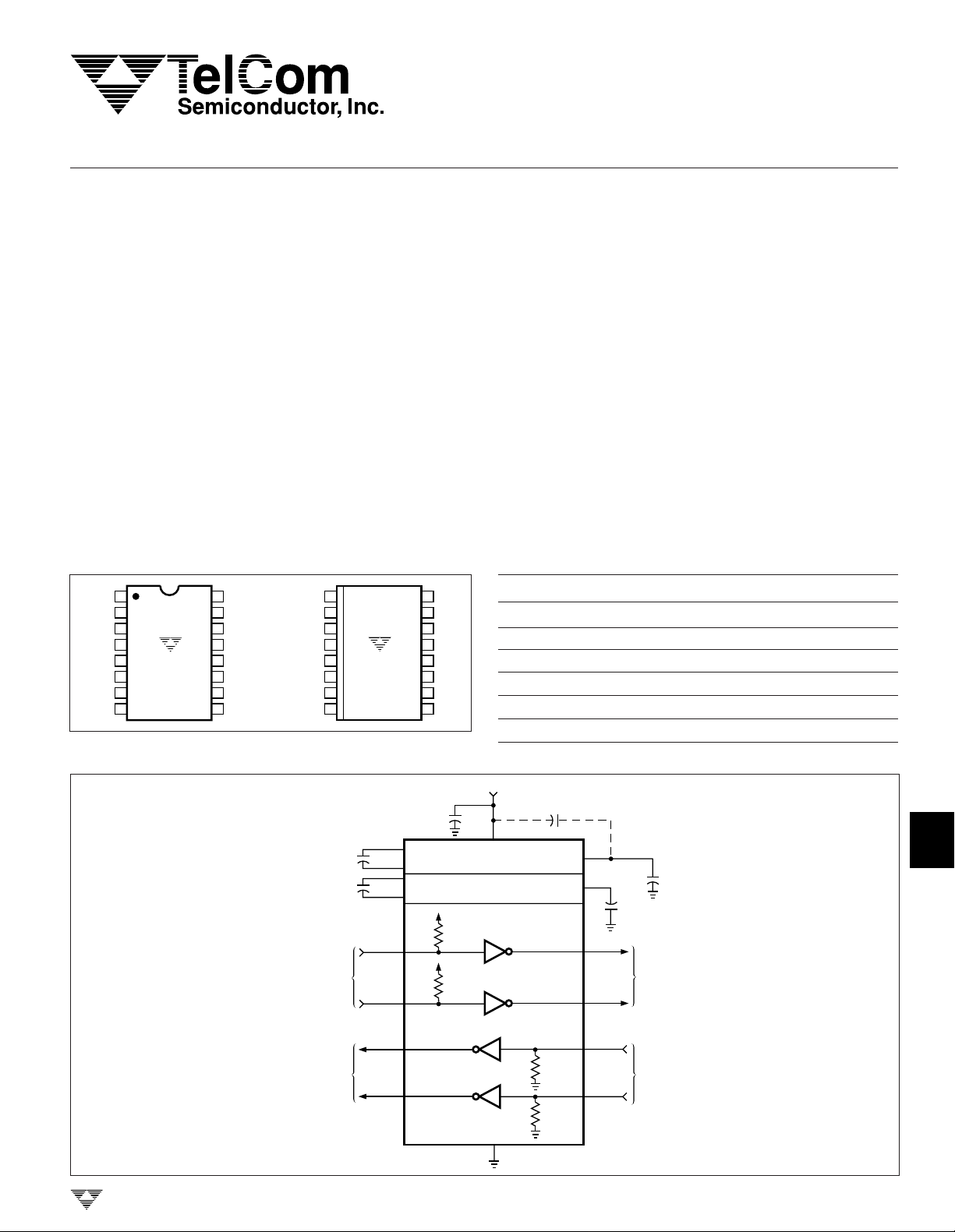
PIN CONFIGURATIONS (DIP AND SOIC)
+
C
1
1
+
2
V
–
C
3
1
+
C
4
2
–
C
V
T2
OUT
R2
TC232CPE
5
2
TC232EPE
–
6
TC232IJE
TC232MJE
7
8
IN
16
V
CC
15
GND
14
T1
OUT
R1
13
IN
12
R1
OUT
T1
11
IN
T2
10
IN
9
R2
OUT
+
C
1
1
+
2
V
–
C
3
1
+
C
4
2
–
C
V
T2
OUT
R2
TC232COE
5
2
TC232EOE
–
6
7
8
IN
16
V
CC
15
GND
14
T1
OUT
R1
13
IN
12
R1
OUT
T1
11
IN
T2
10
IN
9
R2
OUT
GENERAL DESCRIPTION
The TC232 is a dual RS-232 transmitter/receiver that
complies with EIA /TIA RS-232E guidelines and is ideal for
all RS-232 communication links. This device operates from
a 5V power supply and contains two charge pump voltage
converters that produce ±10V power supplies.
The TC232 has four level translators. Two are RS-232
transmitters that convert TTL/CMOS input levels to 9V
RS-232 outputs. The other two translators are RS-232
receivers that convert RS-232 inputs to 5V TTL/CMOS
output levels. The receivers have a nominal threshold of
1.3V, a typical hysteresis of 0.5V, and can operate with
inputs up to ±30V.
ORDERING INFORMATION
Part No. Package Temp. Range
TC232COE 16-Pin SOIC (Wide) 0°C to +70°C
TC232CPE 16-Pin Plastic DIP 0°C to +70°C
TC232EOE 16-Pin SOIC (Wide) – 40°C to +85°C
TC232EPE 16-Pin Plastic DIP – 40°C to +85°C
TC232IJE 16-Pin CerDIP – 25°C to +85°C
TC232MJE 16-Pin CerDIP – 55°C to +125°C
2
3
4
5
TYPICAL APPLICATION
*NOTE:
TELCOM SEMICONDUCTOR, INC.
+
C1
10 µF
+
C2
10 µF
TTL/CMOS
INPUTS
TTL/CMOS
OUTPUTS
C3 can be connected between
V+ and VCC for convenience.
+5V INPUT
+
10 µF
1
+
C
1
3
–
C
1
4
+
C
2
5
–
C
2
+5V
400 kΩ
T1
11
IN
+5V
400 kΩ
T2
10
IN
R1
12
OUT
R2
9
OUT
16
V
CC
+5V TO +10V
VOLTAGE DOUBLER
+10V TO –10V
VOLTAGE INVERTER
T1
T2
R1
R2
GND
15
C3*
10 µF
5 kΩ
+
2
+
V
+10V
+
C4
10 µF
C3*
10 µF
RS-232
OUTPUTS
RS-232
INPUTS
–10V
–
V
6
+
T1
14
OUT
T2
7
OUT
R1
13
IN
R2
8
IN
Ω5 k
6
7
8
TC232-6 10/21/96
6-3
Page 2
TC232
DUAL RS-232 TRANSMITTER/
RECEIVER AND POWER SUPPLY
ABSOLUTE MAXIMUM RATINGS*
VCC............................................................................. +6V
V+........................................................................... +12V
V–........................................................................... +12V
Input Voltages
T1IN, T2IN....................................–0.3 to (VCC +0.3V)
R1IN, R2IN......................................................... ±30V
Output Voltages
T1
, T2
OUT
R1
, R2
OUT
Short Circuit Duration
V+.................................................................... 30sec
V–.................................................................... 30sec
T1
, T2
OUT
...................... (V+ +0.3V) to (V– –0.3V)
OUT
..............................–0.3 to (VCC +0.3V)
OUT
..........................................Continuous
OUT
Package Power Dissipation (TA ≤ 70°C)
CerDIP............................................................890mW
Derate 9.5 mW/°C Above +70°C
Plastic DIP ......................................................840mW
Derate 7 mW/°C Above +70°C
Small Outline (SOIC) ......................................760mW
Derate 7 mW/°C Above +70°C
*Static-sensitive device. Unused devices must be stored in conductive
material. Protect devices from static discharge and static fields. Stresses
above those listed under "Absolute Maximum Ratings" may cause permanent damage to the device. These are stress ratings only and functional
operation of the device at these or any other conditions above those
indicated in the operation sections of the specifications is not implied.
Exposure to absolute maximum rating conditions for extended periods may
affect device reliability.
Storage Temperature Range .................. -65°C to +150°C
ELECTRICAL CHARACTERISTICS: V
= 5V ±10%, TA = operating temperature range, test circuit unless
CC
otherwise noted.
Parameter Test Conditions Min Typ Max Unit
Output Voltage Swing T1
Power Supply Current — 5 10 mA
Input Logic Threshold Low T1IN, T2
Input Logic Threshold High T1IN, T2
Logic Pull-Up Current T1IN, T2IN = 0V — 15 200 µA
RS-232 Input Voltage Operating Range – 30 — +30 V
RS-232 Input Threshold Low VCC = 5V 0.8 1.2 — V
RS-232 Input Threshold High VCC = 5V — 1.7 2.4 V
RS-232 Input Hysteresis 0.2 0.5 1 V
RS-232 Input Resistance TA = +25°C, VCC = 5V 3 5 7 kΩ
TTL/CMOS Output Voltage Low I
TTL/CMOS Output Voltage High I
Propagation Delay RS-232 to TTL or TTL to RS-232 — 0.5 — µsec
Instantaneous Slew Rate CL = 10 pF, RL = 3 kΩ to 7 kΩ,——30V/µsec
Transition Region Slew Rate RL = 3 kΩ, CL = 2500 pF — 3 — V/µsec
Output Resistance VCC = V+ = V– = 0V, V
RS-232 Output — ±10 — mA
Short-Circuit Current
NOTE 1. Sample tested.
, T2
OUT
3 kΩ to Ground
= 3.2 mA — — 0.4 V
OUT
= – 1 mA 3.5 — — V
OUT
TA = +25°C (Note 1)
Measured From +3V to – 3V
or –3V to +3V
Loaded With ±5 ±9 ±10 V
OUT
IN
IN
= ±2V 300 — — Ω
OUT
— — 0.8 V
2——V
6-4
TELCOM SEMICONDUCTOR, INC.
Page 3

DUAL RS-232 TRANSMITTER/
RECEIVER AND POWER SUPPLY
1
TC232
DETAILED DESCRIPTION
The TC232 contains a +5V to ±10V dual charge pump
voltage converter, a dual transmitter and a dual receiver.
+5V to ±10V Dual Charge Pump
Voltage Converter
The TC232 power supply consists of two charge pumps.
One uses external capacitor C1 to double the +5V input to
+10V, with output impedance of about 200Ω. The other
uses C2 to invert +10V to – 10V, with overall output
impedance of 450Ω (including effects of +5V to +10V
doubler impedance).
The clock in the doubler circuit will start at ≈4.2V in the
typical part, but external loads may make this point rise to as
high as 4.5V with a load of 2 kΩ on each of the two output
voltages.
Because of this, use of the doubler and inverter to run
additional external circuits should be limited. The maximum
current should be no more than 2.5 mA from the +10V and
- 10V. in order to guarantee start-up of the doubler clock.
The test circuit employs 22 µF capacitors for C1 to C4,
but the value is not critical. These capacitors usually are lowcost aluminum or tantalum electrolytic capacitors.
Increasing C1 and C2 to 47 µF lowers the output
impedance of the +10V doubler and the - 10V inverter by
the change in the ESR of the capacitors.
Increasing C3 and C4 lowers ripple on the ±10V outputs and 16 kHz ripple on the RS-232 outputs. Where size
is critical, the value of C1 to C4 can be lowered to 1 µF. The
use of a low ESR capacitor will help lower the output ripple
and keep the output impedance of the ±10V as low as
possible.
V+, V– Output Voltages vs Load Current
10
9
8
7
–
V
(V = 4.5V)
CC
6
5
CONDITIONS:
OUTPUT VOLTAGE (|V|)
A) T = +25°C
A
4
B) TRANSMITTER OUTPUTS
OPEN CIRCUIT
3
0 12345678910
+
V
(V = 4.5V)
CC
| I | (mA)
LOAD
+
V
(V = 5V)
CC
–
V
(V = 5V)
CC
The outputs are protected and can be short-circuited to
ground indefinitely.
Dual Receiver
TC232 receivers meet RS-232 input specifications.
Input impedance is between 3 kΩ and 7 kΩ. Switching
thresholds are within the ±3V limits, and the receivers
withstand up to ±30V inputs. RS-232 and TTL/CMOS input
compatible, the receivers have 0.8V VIL and 2.4V VIH with
0.5V hysteresis to reject noise.
The TTL/CMOS compatible receiver output is LOW
when an RS-232 input is greater than 2.4V. It is HIGH
when an input is floating or between +0.8V and – 30V.
2
3
4
5
Dual Transmitter
TC232 transmitters are CMOS inverters driven by ±10V
internally-generated voltages. The input is TTL/CMOS compatible, with a logic threshold of about 26% of VCC (1.3V for
5V VCC). The input of an unused transmitter can be left
unconnected, since an internal 400 kΩ pull-up resistor
connected between the transmitter input and VCC pulls the
input HIGH and forces the unused transmitter output to the
LOW state.
With VCC at 5V, the outputs will go from (V+ – 0.6V) to
V– with no load and will swing ±9V when loaded with 3 kΩ.
The minimum output voltage swing, with VCC at 4.5V and at
maximum ambient temperature, is ±5V. This conforms to
RS-232 specifications for "worst-case" conditions.
EIA/TIA RS-232E specs limit the slew rate at output
to less than 30V/µs.
The powered-down output impedance (VCC = 0V) is
a minimum of 300Ω with ±2V applied to outputs.
TELCOM SEMICONDUCTOR, INC.
TEST CIRCUIT
22 µF
+
C
1
22 µF
+
C
2
22 µF
C
+
RS-232
INPUT
±30V
22 µF
3 kΩ
RS-232
OUTPUT
6
R1
R2
T1
V
CC
GND
OUT
R1
OUT
T1
T2
OUT
+4.5V TO +5.5V
INPUT
16
15
14
13
IN
12
11
IN
10
IN
9
3 kΩ
RS-232
RS-232
INPUT ±30V
TTL/CMOS OUTPUT
TTL/CMOS INPUT
TTL/CMOS OUTPUT
OUTPUT
TTL/CMOS
INPUT
7
TC232
+
1
C
1
+
+
2
V
C
3
–
C
3
1
+
C
4
2
–
C
5
4
2
–
V
6
T2
7
OUT
R2
8
IN
8
6-5
 Loading...