

Page 1
CMOS CURRENT MODE PWM CONTROLLER
1
TC170
FEATURES
■ Low Supply Current With
CMOS Technology................................. 3.8mA Max
■ Internal Reference .............................................5.1V
■ Fast Rise/Fall Times (CL = 1000pF) ............. 50nsec
■ Dual Push-Pull Outputs
■ Direct-Power MOSFET Drive
■ High Totem-Pole Output Drive .................... 300mA
■ Differential Current-Sense Amplifier
■ Programmable Current Limit
■ Soft-Start Operation
■ Double-Pulse Suppression
■ Undervoltage Lockout
■ Wide Supply Voltage Operation ...............8V to16V
■ High Frequency Operation ..........................200kHz
■ Available with Low OFF State Outputs
■ Low Power, Pin-Compatible Replacement for UC3846
ORDERING INFORMATION
Temperature
Part No. Package Range
TC170COE 16-Pin SOIC (Wide) 0°C to +70°C
TC170CPE 16-Pin Plastic DIP (Narrow) 0°C to +70°C
GENERAL DESCRIPTION
The TC170 brings low-power CMOS technology to the
current-mode-switching power supply controller market.
Maximum supply current is 3.8 mA. Bipolar current-mode
control integrated circuits require five times more operating
current.
The dual totem-pole CMOS outputs drive power
MOSFETs or bipolar transistors. The 50nsec typical output
rise and fall times (1000pF capacitive loads) minimize
MOSFET power dissipation. Output peak current is 300mA.
The TC170 contains a full array of system-protection
circuits (see features).
Current-mode control lets users parallel power supply
modules. Two or more TC170 controllers can be slaved
together for parallel operation. Circuits can operate from a
master TC170 internal oscillator or an external system
oscillator.
The TC170 operates from an 8V to 16V power supply.
An internal 2%, 5.1V reference minimizes external component count. The TC170 is pin compatible with the Unitrode
UC1846/2846/3846 bipolar controller.
Other advantages inherent in current-mode control include superior line and load regulation and automatic symmetry correction in push-pull converters.
2
3
4
5
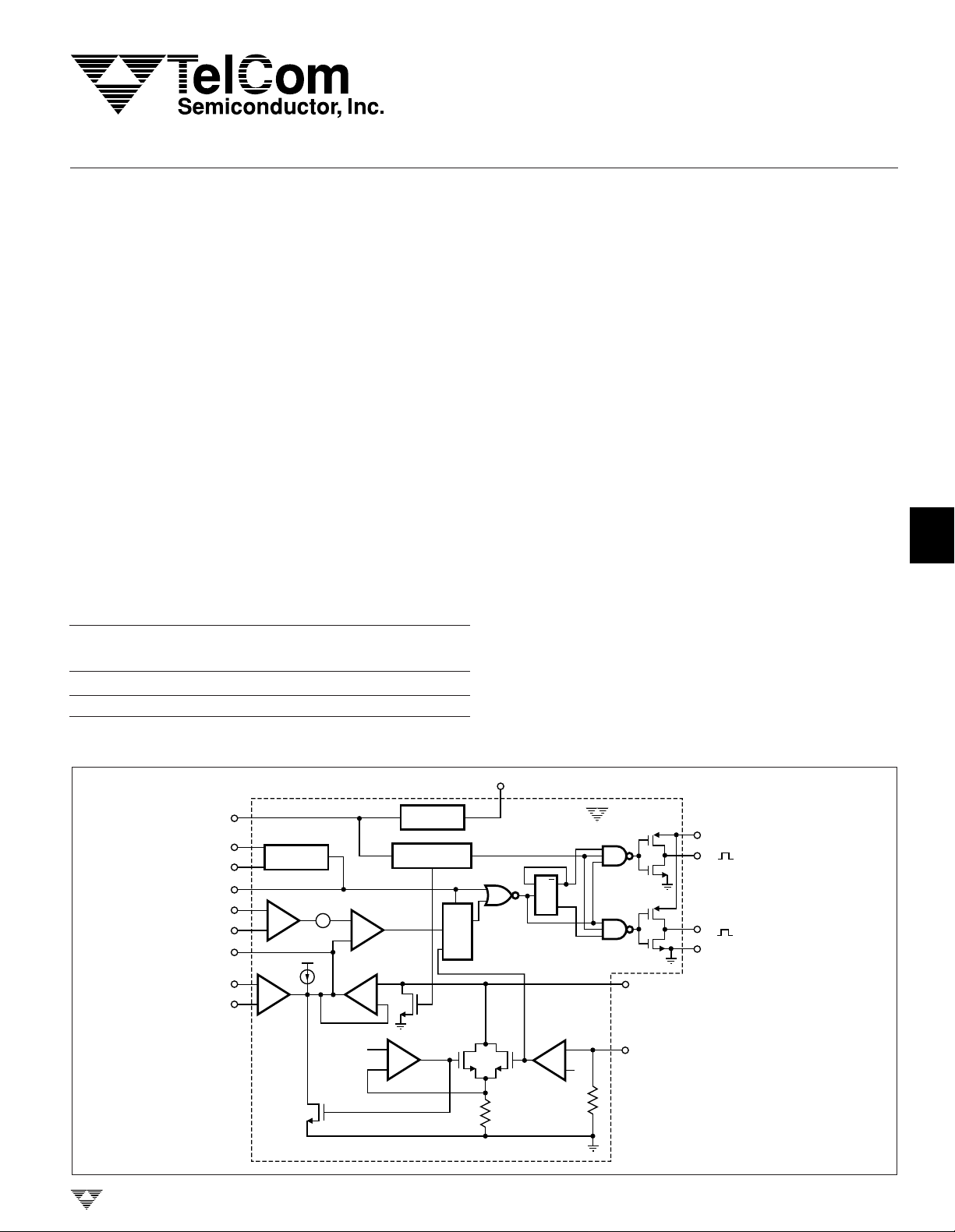
FUNCTIONAL BLOCK DIAGRAM
15
V
IN
9
R
C
SYNC
(–) CURRENT
SENSE INPUT
(+) CURRENT
SENSE INPUT
COMP
(+) ERROR
AMP INPUT
(–) ERROR
AMP INPUT
O
O
8
10
3
4
7
5
6
OSCILLATOR
× 3.15 CURRENT
AMPLIFIER
–
+
V
DD
100µA
+
–
ERROR
AMPLIFIER
TELCOM SEMICONDUCTOR, INC.
–
0.75V
LOCK-UP
AMPLIFIER
Q3
PWM
COMPARATOR
+
+
–
LIMIT BUFFER
AMPLIFIER
350mV
REFERENCE
UNDERVOLTAGE
+
–
Q4
–
+
POSITIVE
FEEDBACK
5.1-VOLT
LOCKOUT
R
S
S
Q
PWM LATCH
Q1
V
REF
Q2
3.5kΩ
2
TC170
DQ
C
Q
SHUTDOWN
COMPARATOR
+
350
–
mV
6kΩ
1
CURRENT LIMIT/
SOFT-START ADJUST
16
SHUTDOWN
NOTE: Outputs low in
OFF state.
13
11
14
12
V
DD
OUTPUT
A ( )
OUTPUT
B ( )
GROUND
6
7
8
TC170-5 10/1/96
4-119
Page 2
TC170
CMOS CURRENT MODE
PWM CONTROLLER
ABSOLUTE MAXIMUM RATINGS*
Supply Voltage ............................................................18V
Output Voltage ................................................ VDD or 18V
Analog Inputs .....................................– 0.3V to VS + 0.3V
Storage Temperature Range ................ – 65°C to +150°C
Lead Temperature (Soldering, 10 sec) ................. +300°C
Maximum Chip Temperature...................................150°C
Plastic Package Thermal Resistance:
θJA (Junction to Ambient)............................. 140°C/W
Operating Temperature Range
Commercial ...........................................0°C to +70°C
*Static-sensitive device. Unused devices must be stored in conductive
material. Protect devices from static discharge and static fields. Stresses
above those listed under Absolute Maximum Ratings may cause permanent damage to the device. These are stress ratings only and functional
operation of the device at these or any other conditions above those
indicated in the operational sections of the specifications is not implied.
Exposure to Absolute Maximum Rating Conditions for extended periods
may affect device reliability.
θJC (Junction to Case) ................................... 70°C/W
ELECTRICAL CHARACTERISTICS: V
= 16V, RO = 24kΩ, CO = 1 nF, TA = 25°C, unless otherwise indicated.
IN
Symbol Parameter Test Conditions Min Typ Max Unit
Reference Voltage
V
V
REF
RTC
Output Voltage I
= 1mA 5 5.1 5.3 V
OUT
Line Regulation VIN = 8V to 16V 5 15 mV
Load Regulation I
= 1mA to 10mA 13 20 mV
OUT
Temperature Coefficient Over Operating Temperature Range 0.4 0.5 mV/°C
Oscillator
Oscillator Frequency 35 42 46 kHz
Voltage Stability VIN = 8V to 16V 1.1 1.5 %/V
Temperature Stability Over Operating Temperature Range 5 10 %
Error Amplifier
V
OS
I
B
V
CMRR
A
VOL
BW Unity Gain Bandwidth 1.2 MHz
CMRR Common-Mode Rejection Ratio V
PSRR Power Supply Rejection Ratio VIN = 8V to 16V 60 dB
Input Offset Voltage 630 mV
Input Bias Current 61nA
Common-Mode Input Voltage VIN = 8V to 16V 0 V
Open-Loop Voltage Gain V
= 1V to 6V 70 dB
OUT
0V to 14V 60 dB
CMV
– 2V V
DD
Current Sense Amplifier
Amplifier Gain Pin 3 = 0V to 1.1V 3 3.15 3.3 V/V
Maximum Differential Input Signal V
Common-Mode Input Voltage 0 V
PIN4
– V
PIN3
≤1.1 V
– 3V V
DD
Current Limit Adjust
Current Limit Offset Voltage 0.5 1 V
I
B
Input Bias Current 1nA
Shutdown Terminal
V
TB
V
IN
Threshold Voltage 0.3 0.35 0.4 V
Input Voltage Range 0 V
DD
V
Minimum Latching Current at Pin 1 125 µA
Maximum Nonlatching Current at Pin 1 50 µA
Output Stage
V
DD
V
OL
V
OL
Output Voltage Pin 13 V
Output Low Level I
Output Low Level I
= 20mA 0.4 V
SINK
= 100mA 2 V
SINK
– 0. 5 V
IN
V
IN
+ 0.5 V
IN
4-120
TELCOM SEMICONDUCTOR, INC.
Page 3
CMOS CURRENT MODE
PWM CONTROLLER
1
TC170
ELECTRICAL CHARACTERISTICS (Cont.):
VIN = 16V, RO = 24kΩ, CO = 1nF, TA = 25°C, unless otherwise indicated.
Symbol Parameter Test Conditions Min Typ Max Unit
Output Stage (Cont.)
V
OH
V
OL
t
R
t
F
Output High Level I
Output High Level I
= 20mA V
SOURCE
= 100mA V
SOURCE
– 1V V
DD
– 4V V
DD
Output Rise Time CL = 1000pF 50 150 nsec
Output Fall Time CL = 1000pF 50 150 nsec
Undervoltage Lockout
Start-Up Threshold 7.15 7.7 8.25 V
Threshold Hysteresis 0.5 0.75 1 V
Supply
ISStandby Supply Current 2.7 3.8 mA
PIN DESCRIPTION
Pin No.
(16-Pin PDIP) Symbol Description
1 SOFT START/I
2V
3– I
4+ I
OUT Reference supply output of 5.1 volts. It can supply a minimum of 10mA.
REF
IN – Current Sense Input. Inverting input for sensing peak current of the pass transistor
SENSE
IN + Current Sense Input. Non-inverting input used in conjunction with pin 3. This senses the
SENSE
5 + ERROR AMP IN + Error Amp In. Non-inverting input for output voltage regulation.
6 – ERROR AMP IN – Error Amp In. Inverting input of the amplifier for the reference voltage.
7 CMPTR For compensation of the feedback loop response.
8C
9R
O
O
10 SYNC For PWM controller oscillator synchronization of two or more controllers. or as a clock input
11 OUTPUT A A output drive of phase A from push pull transistors.
12 GND Ground return for all input and output pins.
13 V
DD
14 OUTPUT B Output of phase B from push pull transistors.
15 V
IN
16 SHUTDOWN Input pin to disable both output drives to 0V OFF.
Soft Start Adjust / Current Limit. For setting the peak current threshold of sense inputs (pins
LIM
3 and 4). Second function of this pin is Soft-Start Adjust.
through series sense current monitor resistor.
positive end of current monitor resistor.
Timing capacitor (CO) input to set oscillator frequency in conjunction with pin 9, RO, resistor
input. Second function is for setting crossover dead time of pin 11and 14 outputs.
Timing resistor (RO) input to set oscillator frequency by setting constant current charge rate
to charge capacitor CO.
to sync oscillator from external signal.
Supplies power to operate the output drivers only.
Voltage bias supply for all TC170 circuits except the output transistors.
2
3
4
5
6
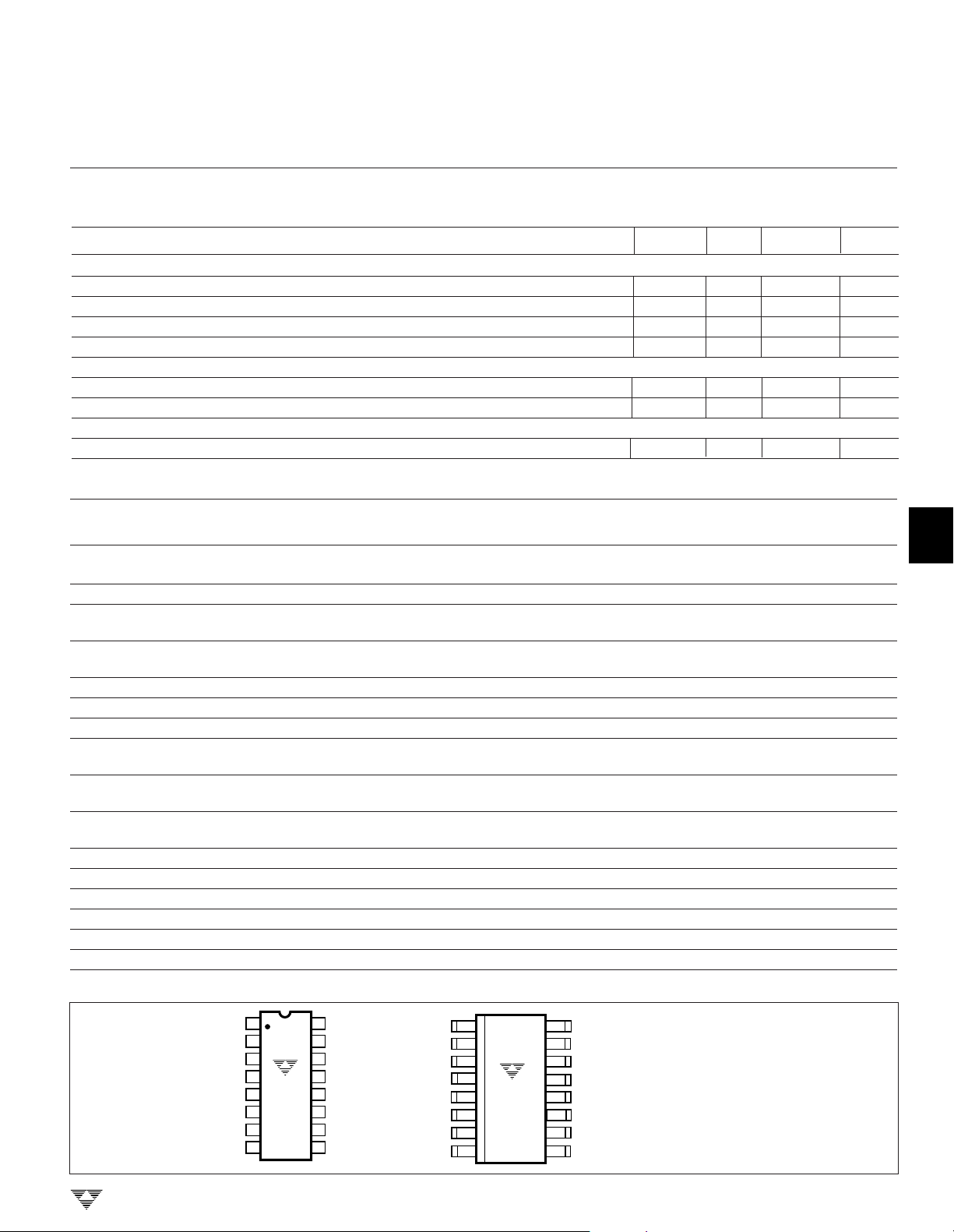
PIN CONFIGURATIONS (DIP and SOIC)
SOFT START/
I
LIM
OUT
V
REF
– I
SENSE
+ I
SENSE
+ ERROR AMP IN
– ERROR AMP IN
CMPTR
C
1
2
IN
3
IN
4
TC170
5
CPE
6
7
8
O
SHDN
16
V
15
14
OUTPUT B
V
13
12
GND
11
OUTPUT A
10
SYNC
R
9
IN
DD
O
TELCOM SEMICONDUCTOR, INC.
C
INT
V
SS
C
AZ
BUF
ACOM
–
C
REF
+
C
REF
–
V
REF
1
2
3
4
TC170COE
5
6
7
8
16
15
14
13
12
11
10
9
V
DD
DIGITAL GND
CMPTR OUT
B
A
+
V
IN
–
V
IN
+
V
REF
NOTE: Outputs LOW in "OFF" state.
7
8
4-121
Page 4

TC170
CMOS CURRENT MODE
PWM CONTROLLER
Peak Current Limit Setup
Resistors R1 and R2 at the current limit input (pin 1)
set the TC170 peak current limit (Figure 1). The potential at
pin 1 is easily calculated:
V1 = V
REF
R1 should be selected first. The shutdown circuit feature is not latched for (V
latched for currents greater than 125µA.
The error amplifier output voltage is clamped from
going above V1 through the limit buffer amplifier. Peak
current is sensed by RS and amplified by the current
amplifier which has a fixed gain of 3.15.
I
, the peak current limit, is the current that causes
PCL
the PWM comparator noninverting input to exceed V1, the
potential at the inverting input. Once the comparator trip
point is exceeded, both outputs are disabled.
I
is easily calculated:
PCL
I
=
PCL
where:
V1 = V
V
REF
3.15 = Gain of current-sense amplifier
0.75V = Current limit offset
Both driver outputs (pins 11 and 14) are OFF (LOW)
when the peak current limit is exceeded. When the sensed
current goes below I
R2
R1 + R2
– 0.35)/R1 < 50µA and is
REF
V1 – 0.75V
3.15 (RS)
REF
R2
R1 + R2
= Internal voltage reference = 5.1V
, the circuit operates normally.
PCL
The input pulse to pin 16 should be at least 500 nsec
wide and have an amplitude of at least 1V in order to get the
minimum propagation delay from input to output. If these
parameters are met, the delay should be less than
600nsec at 25°C; however, the delay time will increase as
the device temperature rises.
Soft Restart From Shutdown
A soft restart can be programmed if nonlatched shutdown operation is used.
A capacitor at pin 1 will cause a gradual increase in
potential toward V1. When the voltage at pin 1 reaches
0.75V, the PWM latch set input is removed and the circuit
establishes a regulated output voltage. The soft-start operation forces the PWM output drivers to initially operate with
minimum duty cycle and low peak currents.
Even if a soft start is not required, it is necessary to
insert a capacitor between pin 1 and ground if the current I
is greater than 125µA. This capacitor will prevent "noise
triggering" of the latch, yet minimize the soft-start effect.
Soft-Start Power-Up
During power-up, a capacitor at R1, R2 initiates a softstart cycle. As the input voltage (pin 15) exceeds the
undervoltage lockout potential (7.7V), Q4 is turned OFF,
ending undervoltage lockout. Whenever the PWM comparator inverting input is below 0.5V, both outputs are
disabled.
When the undervoltage lockout level is passed, the
capacitor begins to charge. The PWM duty cycle increases
until the operating output voltage is reached. Soft-start
operation forces the PWM output drivers to initially operate
with minimum duty cycle and low peak current.
L
Output Shutdown
The TC170 outputs can be turned OFF quickly through
the shutdown input (pin 16). A signal greater than 350 mV
at pin 16 forces the shutdown comparator output HIGH.
The PWM latch is held set, disabling the outputs.
Q2 is also turned ON. If V
positive feedback through the lock-up amplifier and Q1
keeps the inverting PWM comparator inverting input below
0.75V. Q3 remains ON even after the shutdown input
signal is removed, because of the positive feedback. The
state can be cleared only through a power-up cycle. Outputs will be disabled whenever the potential at pin 1 is
below 0.75V.
The shutdown terminal gives a fast, direct way to disable the TC170 output transistors. System protection and
remote shutdown applications are possible.
4-122
/R1 is greater than 125µA,
REF
Current-Sense Amplifier
The current-sense amplifier operates at a fixed gain of
3.15. Maximum differential input voltage (V
1.1V. Common-mode input voltage range is 0V to VIN – 3V.
Resistive-sensing methods are shown in Figure 2. In
Figure 2(A), a simple RC filter limits transient voltage spikes
at pin 4, caused by external output transistor-collector
capacitance. Transformer coupling (Figure 3) offers isolation and better power efficiency, but cost and complexity
increase.
In order to minimize the propagation delay from the input
to the current amplifier to the output terminals, the current
ramp should be in the order of 1 µs in width (min). Typical
time delay values are in the 300 to 400nsec region at 25°C.
The delay time increases with device temperature so that at
50°C, the delay times may be increased by as much as
100nsec.
TELCOM SEMICONDUCTOR, INC.
PIN4
– V
PIN3
) is
Page 5

CMOS CURRENT MODE
(B)
g
PWM CONTROLLER
1
TC170
SWITCH
CURRENT
4
3
RS
7
5
6
3.15 CURRENT-SENSE
×
AMPLIFIER
+
–
ERROR
AMPLIFIER
+
–
–
0.75V
V
DD
+
100 Aµ
Q3
350mV
V1
PWM COMPARATOR
+
–
Q4
+
LIMIT
BUFFER
AMPLIFIER
–
+
–
LOCK-UP
AMPLIFIER
POSITIVE
FEEDBACK
FROM
UNDERVOLTAGE
LOCKOUT
Q1
Q2
10
R
Q
S
S
PWM LATCH
SHUTDOWN
COMPARATOR
+
–
"A" = 1
OUTPUT
OFF (LOW)
V
REF
6k
5.1V
2
R1
1
R2
16
2
3
V1
4
×
3.15 CURRENTSENSE
AMPLIFIER
TC170
(A) Ground Reference
TC170
4
+
–
3
*OPTIONAL RC FILTER
I
L
Figure 1. R1 and R2 Set Maximum Peak Output Current
I
R*
C
RS
Figure 2. Resistive Sensing
3.5k
I
×
3.15 CURRENTSENSE AMPLIFIER
4
+
–
3
TC170
Above-Ground Resistive Sensin
350mV
RS
V
5
6
OUT
7
TELCOM SEMICONDUCTOR, INC.
8
4-123
Page 6

TC170
MASTER
R
O
SYNC CMPTR
SLAVE
9
8
9
8
210 7
7
1/2 TC4427
V
DD
TC170
10
C
O
V
REF
C
O
R
O
CMPTRSYNC
TC170
×
3.15 CURRENT–
SENSE AMPLIFIER
4
+
–
TC170
Figure 3 Transformer Isolated Current Sense
+
V
S
–
3
IS • RS
=
V
S
N
Undervoltage Lockout
The undervoltage lockout circuit forces the TC170 outputs OFF (low) if the supply voltage is below 7.7V. Threshold
hysteresis is 0.75V and guarantees clean, jitter-free turn-on
and turn-off points. The hysteresis also reduces capacitive
filtering requirements at the PWM controller supply input
(pin 15).
N
1
I
S
CMOS CURRENT MODE
PWM CONTROLLER
Circuit Synchronization
Current-mode-controlled power supplies can be operated in parallel with a common load. Paralleled converters
will equally share the load current. Voltage-mode controllers unequally share the load current, decreasing system
reliability.
Two or more TC170 controllers can be slaved together for parallel operation. Circuits can operate from a
master TC170 internal oscillator with an external driver
(Figure 4). Devices can also be slaved to an external
oscillator (Figure 5). Disable internal slave device oscillators by grounding pin 8. Slave controllers derive an oscillator from the bidirectional synchronization output signal at
pin 10.
Pin 10 is bidirectional in that it is intended to be both a
sync output and input. This is accomplished by making the
output driver "weak." This is advantageous in that it eliminates an additional pin from the package but does not
enable the device to directly drive another device. In order
to make it an effective driver, a buffer is required (Figure 4).
In order to use pin 10 as a sync input, it is necessary to
overcome the internal driver. This requires a pulse with an
amplitude equal to VIN. Since VIN must be above 8.25V for
the undervoltage lockout to be disabled, a CMOS or opencollector TTL driver should be used.
Figure 4. Master/Slave Parallel Operation
EXTERNAL*
OSCILLATOR
*PULSE WIDTH OF
OSCILLATOR IS = T
Figure 5. External Clock Synchronization
V
DD
TC4427
D
1/2
10
10
15
V
IN
TC170
SYNC
V
REF
29
+
V
S
15
V
IN
SYNC
TC170
V
REF
29
8
C
O
R
O
C
O
R
O
4-124
TELCOM SEMICONDUCTOR, INC.
Page 7

CMOS CURRENT MODE
PWM CONTROLLER
1
TC170
V
2.3V
R
O
9
R
O
Figure 6 . Oscillator Circuit
10
SYNC
DISCHARGE
CURRENT
2.3V 4.3V
1 mA
I
CHARGE
8
C
O
Oscillator Frequency and Output Dead Time
The oscillator frequency for RO = 24kΩ and
CO= 1000pF is:
1.27 2800 C
FO =
[
ROC
where: RO = Oscillator Resistor (Ω)
The oscillator resistor can range from 5 kΩ to 50 kΩ.
Oscillator capacitor can range from 250 pF to 1000 pF.
Figure 7 shows typical operation for various resistance and
capacitance values.
During transitions between the two outputs, simultaneous conduction is prevented. Oscillator fall time controls
the output off, or dead time (Figure 6).
Dead time is approximately:
TD =
2000 [CO]
1 –
–
2
R
O
CO = Oscillator Capacitor (F)
FO = Oscillator Frequency (Hz)
2.3
(
R
O
]
COCO + 150 × 10
O
)
O
–12
DD
1
F
PIN 8
+
2.3V
–
PIN 10
50
45
40
35
30
25
20
15
10
OSCILLATOR RESISTANCE (kΩ)
5
0 20 40 60 80 100 120 140 160 180 200
OSCILLATOR FREQUENCY (kHz)
Figure 7. Oscillator Frequency vs Oscillator Resistance
where: RO = Oscillator Resistor (kΩ)
CO = Oscillator Capacitor (pF)
TD = Output Dead Time (sec)
O
ON-TIME
OUTPUT DEAD TIME (TD)
TA= +25°C
250pF
750pF1000pF
500pF
2
3
4
5
6
7
TELCOM SEMICONDUCTOR, INC.
Maximum possible duty cycle is set by the dead time.
8
4-125
Page 8

TC170
TYPICAL CHARACTERISTICS
CMOS CURRENT MODE
PWM CONTROLLER
Output Rise and Fall Times
TA = +25°C
C
VS = 16V
LOAD
= 500pF
DIV
5V
50nsec
DIV
Output Rise and Fall Times
TA = +25°C
C
VS = 16V
LOAD
= 1800pF
5V
DIV
5 nsec
DIV
Output Rise and Fall Times
TA = +25°C
C
VS = 16V
LOAD
= 1000pF
5V
DIV
50nsec
DIV
4-126
TELCOM SEMICONDUCTOR, INC.
 Loading...