

Page 1

TC170
E
SHDN
SO
/
SE
SE
N
R
N
.
6
5
0COE
/
SE
SE
N
R
N
)
)
CMOS Current Mode PWM Controller
Features
• Low Supply Current With CMOS Technology:
3.8mA Max
• Internal Reference: 5.1V
• Fast Rise/Fall Times(C
= 1000pF): 50nsec
L
• Dual Push-Pull Outputs
•Direct-PowerMOSFETDrive
• High Totem-Pole Output Drive: 300mA
• Differential Current-Sense Amplifier
• Programmable Current Limit
• Soft-Start Operation
• Double-Pulse Suppression
• Undervoltage Lockout
• Wide Supply Voltage Operation: 8V to 16V
• High Frequency Operation: 200kHz
• Available with Low OFF StateOutputs
• Low Power, Pin-Compatible Replacement for
UC3846
Applications
• Switching Power Supplies
• DC/DC Converters
• Motor Control
General Description
The TC170 offers maximum supply current of 3.8mA.
Bipolar current-mode control integrated circuits require
five times more operating current.
The dual t otem-pole CMOS outputs drive power
MOSFETs or bipolar transistors. The 50nsec typical
output rise and fall times (1000pF capacitive loads)
minimize MOSFET power dissipation. Output peak
current is 300mA.
The TC170 contains a full array of system-protection
circuits (see Features Section).
Current-mode control lets users parallel power supply
modules.Two or more TC170 controllers can be slaved
together for parallel operation. Ci rcuits can operate
from a master TC170 internal oscillator or an external
system oscillator.
The TC170 operates from an 8V to 16V power supply.
An internal 2%, 5.1V r eference minimizes external
component count. The TC170 is pin compatible with
the Unitrode UC1846/UC2846/UC3846 bipolar
controller.
Other advantages inherent in current-mode control
includesuperior line and load regulation and automatic
symmetry correction in push-pull converters.
Device Selection Table
Part Number Package Temp. Range
TC170COE 16-Pin SOIC (Wide) 0°C to +70°C
TC170CPE 16-Pin PDIP (Narrow) 0°C to +70°C
Package Type
16-Pin PDIP (Narrow
FT START
V
REF
– I
EN
+ I
EN
+ ERROR AMP I
– ERROR AMP I
MPT
NOTE: Outputs LOW in "OFF" state
TC170CP
1
1
FT START
V
REF
– I
EN
+ I
EN
+ ERROR AMP I
– ERROR AMP I
MPT
16-Pin SOIC (Wide
16
15
14
TC17
13
12
10
11
9
SHDN
V
IN
OUTPUT B
V
DD
GND
OUTPUT A
SYNC
R
O
2002 Microchip TechnologyInc. DS21395B-page 1
Page 2
TC170
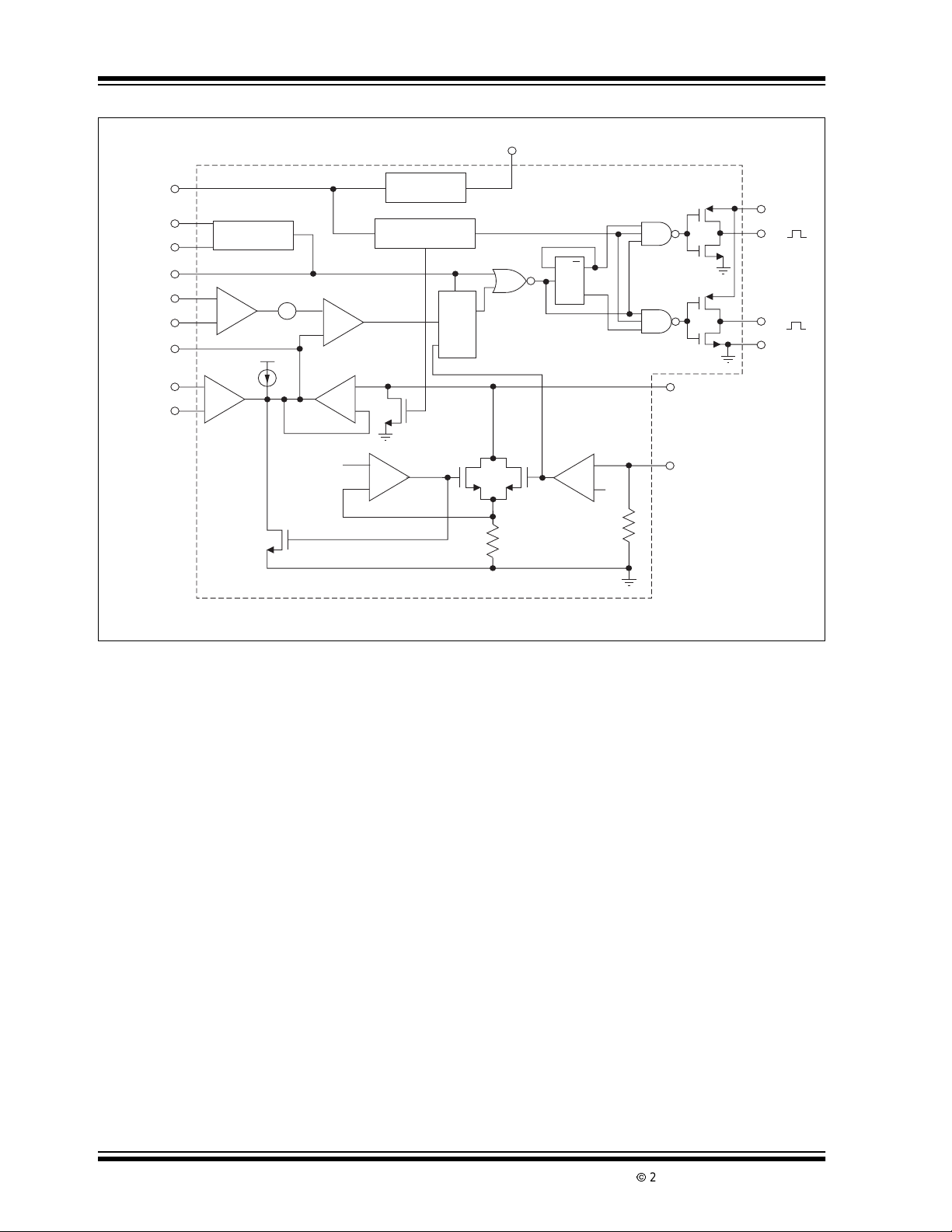
Functional Block Diagram
15
V
IN
9
R
Sync
(–) Current
Sense Input
(+) Current
Sense Input
Comp
(+) Error
Amp Input
(–) Error
Amp Input
O
C
O
10
8
3
4
7
5
6
Oscillator
–
+
100µA
+
–
Error
Amplifier
x 3.15 Current
Amplifier
–
0.75V
V
DD
Q3
Lock-up
Amplifier
+
+
–
Limit Buffer
Amplifier
350mV
PWM
Comparator
+
–
Q4
–
+
Positive
Feedback
5.1-Volt
Reference
Undervoltage
Lockout
S
S
R
Q
PWM Latch
Q1
V
REF
Q2
3.5kΩ
2
13
11
14
12
V
DD
Output
A ( )
Output
B ( )
Ground
DQ
C
Q
Shutdown
Comparator
+
–
6kΩ
TC170
350
mV
1
Current Limit/
Soft-Start Adjust
16
Shutdown
NOTE: Outputs low in OFF state.
DS21395B-page 2
2002 Microchip TechnologyInc.
Page 3
TC170
1.0 ELECTRICAL
CHARACTERISTICS
*Stresses above those listed under "Absolute Maximum
Ratings" may cause permanent damage to the device. These
are stress ratings only and functional operation of the device
at these or any other conditions above those indicated in the
Absolute Maximum Ratings*
Supply Voltage.......................................................18V
Output Voltage ........................................... V
Analog Inputs ..................................-0.3V to V
DD
S
or 18V
+0.3V
operation sections of the specifications is not implied.
Exposure to Absolute Maximum Rating conditions for
extended periods may affectdevice reliability.
Package Thermal Resistance:
SOIC (Wide) θ
SOIC (Wide) θ
PDIP (Narrow) θ
PDIP (Narrow) θ
.....................................105°C/W
JA
.......................................23°C/W
JC
....................................95°C/W
JA
....................................55°C/W
JC
Operating Temperature Range ...............0°C to +70°C
StorageTemperature Range..............-65°C to +150°C
TC170 ELECTRICAL SPECIFICATIONS
Electrical Characteristics: VIN=16V,RO=24kΩ,CO= 1nF, TA= 25°C, unless otherwise noted.
Symbol Parameter Min Typ Max Units Test Conditions
Reference Voltage
V
REF
Reference Voltage 5 5.1 5.3 V I
Line Regulation 5 15 mV V
Load Regulation 13 20 mV I
V
RTC
Temperature Coefficient 0.4 0.5 mV/°C Overoperating temperature range.
Oscillator
F Oscillator Frequency 35 42 46 kHz
VC
TC
Voltage Stability 1.1 1.5 %/V VIN=8Vto16V
OSC
T emperature Stability 5 10 % Over operating temperature range.
OSC
Error Amplifier
V
OS
I
B
V
CMRR
A
VOL
Input Offset Voltage ±30 mV
Input Bias Current ±1 nA
Common-Mode Input Voltage 0 VDD–2V V VIN=8Vto16V
Open-Loop Voltage Gain 70 dB V
BW Unity Gain Bandwidth 1.2 MHz
CMRR Common-Mode RejectionRatio 60 dB V
PSRR Power Supply Rejection Ratio 60 dB V
Current Sense Amplifier
A
V
V
IAMP
DM
CM
Amplifier Gain 3 3.15 3.3 V/V Pin 3 = 0V to 1.1V
MaximumDifferential Input Signal ≤ 1.1 V V
Common-Mode Input Voltage 0 VDD–3V V
Current LimitAdjust
V
OS
I
B
Current Limit Offset Voltage 0.5 1 V
Input Bias Current 1 nA
Shutdown Terminal
V
TH
V
IN
I
L
I
L
Threshold Voltage 0.3 0.35 0.4 V
Input Voltage Range 0 V
DD
MinimumLatching Currentat Pin 1 125 µA
MaximumNonlatchingCurrent at Pin 1 50 µA
V
=1mA
OUT
=8Vto16V
IN
= 1mA to 10mA
OUT
=1Vto6V
OUT
=0Vto14V
CMV
=8Vto16V
IN
PIN4–VPIN3
2002 Microchip TechnologyInc. DS21395B-page 3
Page 4
TC170
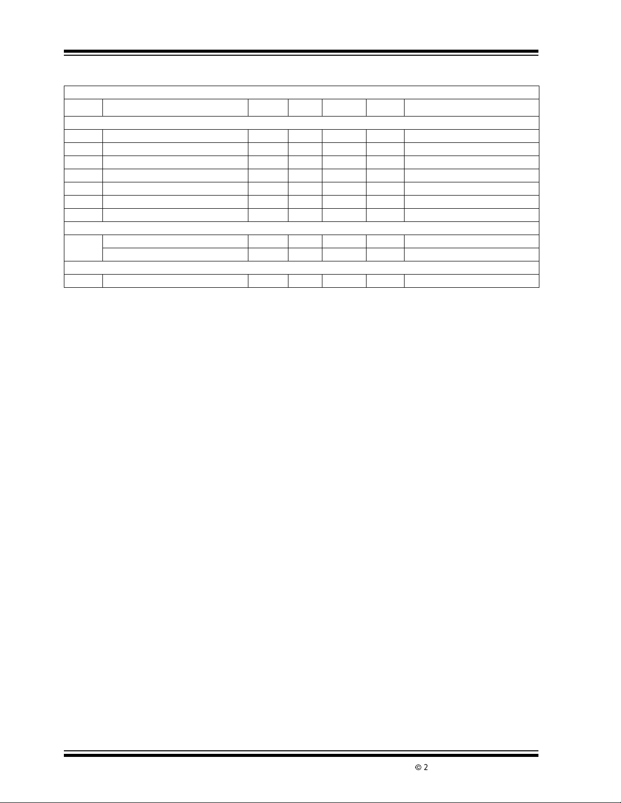
TC170 ELECTRICAL SPECIFICATIONS (CONTINUED)
Electrical Characteristics: VIN=16V,RO=24kΩ,CO= 1nF,TA= 25°C, unless otherwise noted.
Symbol Parameter Min Typ Max Units Test Conditions
Output Stage
V
DD
V
OL
V
OL
V
OH
V
OL
t
R
t
F
OutputVoltage VIN–0.5 V
OutputLow Level 0. 4 V I
OutputLow Level 2 V I
OutputHighLevel VDD–1V V I
OutputHighLevel VDD–4V V I
OutputRiseTime 50 150 nsec CL= 1000pF
OutputFallTime 50 150 nsec CL= 1000pF
Undervoltage Lockout
Start-Up 7.15 7.7 8.25 V Threshold
Threshold Hysteresis 0.5 0.75 1 V
Supply
I
S
StandbySupplyCurrent 2.7 3.8 mA
VIN+0.5 V Pin13
IN
=20mA
SINK
= 100mA
SINK
SOURCE
SOURCE
=20mA
=100mA
DS21395B-page 4
2002 Microchip TechnologyInc.
Page 5

TC170
2.0 PIN DESCRIPTIONS
ThedescriptionsofthepinsarelistedinTable2-1.
TABLE 2-1: PIN FUNCTION TABLE
Pin No.
(16-Pin PDIP,
SOIC)
1SOFTSTART/I
2V
3-I
4+I
5 +ERROR AMP IN +Error Amp In. Non-inverting input for output voltage regulation.
6 -ERROR AMP IN -Error Amp In. Inverting input of the amplifier for the reference voltage.
7 CMPTR For compensation of the feedback loop response.
8C
9R
10 SYNC ForPWM controlleroscillator synchronizationof two or morecontrollers.Or as a clockinput to
11 OUTPUT A A output drive of phase A from push pulltransistors.
12 GND Ground return for all input and output pins.
13 V
14 OUTPUT B Output of phase B from push pull transistors.
15 V
16 SHDN Input pin to disable both output drivesto 0V OFF.
Symbol Description
Soft Start Adjust/Current Limit. For setting the peak current threshold of sense inputs (pins 3
LIM
and 4). Second function of this pin is Soft-Start Adjust.
OUT Reference supply outputof 5.1 volts.It can supply a minimum of 10mA.
REF
IN -CurrentSenseInput. Invertinginputforsensing peak current of the pass transistor through
SENSE
SENSE
O
O
DD
IN
seriessensecurrent monitor resistor.
IN +Current Sense Input. Non-inverting input used in conjunction with pin 3. This senses the
positive end of current monitor resistor.
Timing capacitor (CO) input to set oscillator frequency in conjunction with pin 9, RO,resistor
input. Second function is for setting crossover dead time of pin 11and 14 outputs.
Timing resistor (RO) input to set oscillator frequency by setting constant current charge rate to
charge capacitor C
sync oscillator from externalsignal.
Supplies power to operate the output drivers only.
Voltage bias supply for all TC170 circuits except the output transistors.
.
O
2002 Microchip TechnologyInc. DS21395B-page 5
Page 6

TC170
3.0 DETAILED DESCRIPTION
3.1 Peak Current Limit Setup
ResistorsR1and R2 at the c urrent limit input (pin 1) set
the TC170 peak current limit (Figure 3-1). Thepotential
at pin 1 is easily c alculated:
V1 = V
REF
R1 should be selected first. The shutdown circuit
feature is not latched for (V
is latched for currents greater t han 125µA.
The error amplifier output voltage is clamped from
going above V1 through the limit buffer amplifier. Peak
current is sensed by RS and amplified by the current
amplifier which has a fixed gain of 3.15.
I
, the peak current limit, is t he current that causes
PCL
the PWM comparator noninverting input to exceed V1,
the potential at the inverting input. Once t he
comparator trip point is exceeded, both outputs are
disabled.
I
is easily calculated:
PCL
I
=
PCL
where:
V1 = V
REF
V
= Internal voltage reference = 5.1V
REF
3.15 = Gain of current-sense amplifier
0.75V = Current limit offset
Both driver outputs (pins 11 and 14) are OFF (LOW)
when the peak current limit is exceeded. W hen t he
sensed current goes below I
normally.
3.2 Output Shutdown
The TC170 outputscan be turned OFFquickly through
the shutdown input (pin 16). A signal greater than
350mV at pin 16 forces the shutdown comparator
output HIGH. The PWM l atch is held set, disabling the
outputs.
Q2is also turned ON. If V
positive feedback through the lockup amplifier and Q1
keeps the inverting PWM comparator inverting input
below 0.75V. Q3 remains ON even after t he shutdown
input signal is r emoved, because of the positive
feedback. The state can be cleared only through a
power-up cycle. Outputs will be disabled whenever the
potential at pin 1 is below 0.75V.
The shutdown t erminal gives a fast, di rect way to
disable the TC170 output t ransistors. System protection and remote shutdown applications are possible.
R2
R1 + R2
V1–0.75V
3.15 (RS)
R2
R1 + R2
– 0.35)/R1 < 50µAand
REF
, the circuit operates
PCL
/R1isgreaterthan125µA,
REF
The input pulse to pin 16 should be at least 500nsec
wide and have an amplitude of at least 1V in order to
get the minimum propagation delay from input to
output. If these parameters are met, the delay should
be less than 600nsec at 25°C; however, the delay time
will increase as the device temperature rises.
3.3 Soft Restart From S hutdown
A soft restart can be programmed if nonlatched
shutdown operation is used.
A capacitor at pin 1 will cause a gradual increase in
potentialtoward V1. When the voltage at pin 1 reaches
0.75V, the PWM latch set input is removed and the
circuit establishesa regulated output voltage.The softstartoperationf orces the PWM outputdriverstoinitially
operate with minimum duty cycle and low peak
currents.
Even if a soft start is not required, it is necessary to
insert a capacitor between pin 1 and ground if the
current I
prevent "noise triggering" of the latch, yet minimize the
soft-start effect.
is greater than 125µA. This capacitor will
L
3.4 Soft-Start Power-Up
During power-up, a capacitor at R1, R2 initiates a softstart cycle. As the input voltage (pin 15) exceeds the
undervoltage lockout potential (7.7V), Q4 is turned
OFF, ending undervoltage lockout. Whenever t he
PWM comparator inverting input is below 0.5V, both
outputs are disabled.
When the undervoltage l ockout level is passed, the
capacitor begins to charge. The PWM duty cycle
increasesuntil the operatingoutput voltageis reached.
Soft-start operation forces the PWM output drivers to
initially operate with minimum duty cycle and low peak
current.
3.5 Current-Sense Amplifier
The current-sense amplifier operates at a fixed gain
of 3.15. M aximum differential input voltage (V
V
) is 1.1V. Common-mode input voltage range is
PIN3
0V to V
Resistive-sensing methods are shown in Figure3-2
and Figure 3-3. I n Figure 3-2, a simple RC filter limits
transient voltage spikes at pin 4, caused by external
output transistor-collector capacitance. Transformer
coupling (Figure 3-4) o ffers isolation and better power
efficiency, but cost and complexity increase.
In order to minimize the propagation delay from the
inputto the current amplifierto the output terminals,the
current ramp s hould be in the order of 1µsec in width
(min). Typical time delay values are in the 300 to
400nsec region at 25°C. The delay t ime increases with
device temperature so that at 50°C, the delay times
may be increased by as much as 100nsec.
IN
–3V.
PIN4
–
DS21395B-page 6
2002 Microchip TechnologyInc.
Page 7

FIGURE 3-1: R1 AND R2 SET MAXIMUM PEAK OUTPUT CURRENT
TC170
Switch
Current
RS
x 3.15 Current Sense
Amplifier
4
+
3
–
7
Error
Amplifier
5
+
6
–
–
0.75V
V
DD
Q3
TC170
+
100µA
350mV
PWM Comparator
V1
Limit
Buffer
Amplifier
+
–
Lock-Up
Amplifier
–
+
Q4
+
–
Positive
Feedback
From
Undervoltage
Lockout
Q1
I
3.5kΩ
L
Q2
10
R
Q
S
S
PWM Latch
Shutdown
Comparator
+
–
350mV
"A" = 1
Output
Off (Low)
V
REF
6kΩ
5.1V
2
R1
1
R2
16
V1
FIGURE 3-2: GROUND REFERENCE
RESISTIVE SENSING
x 3.15 Current Sense
Amplifier
TC170
4
+
–
3
*Optional RC Filter
R*
C
RS
FIGURE 3-3: ABOVE GROUND
RESISTIVE SENSING
I
x 3.15 Current Sense
Amplifier
I
TC170
RS
4
+
–
3
V
OUT
2002 Microchip TechnologyInc. DS21395B-page 7
Page 8

TC170
FIGURE 3-4: TRANSFORMER
ISOLAT E D CURRENT
SENSE
x 3.15 Current Sense
Amplifier
TC170
4
+
–
+
V
S
–
3
I
• RS
S
=
V
S
N
N1
I
S
3.6 Undervoltage Lockout
The undervoltage lockout circuit forces the TC170
outputs OFF (low) i f the supply voltage is below 7.7V.
Threshold hysteresis is 0.75V and guarantees clean,
jitter-free turn-on and turnoff points. The hysteresis
also reduces capacitive filtering requirements at the
PWM controller supply i nput (pin 15).
3.7 Circuit Synchronization
Current-mode-controlled power supplies can be
operated in parallel with a common load. Paralleled
converters will equally share the load current. Voltagemode controllers unequally share the load current,
decreasing system reliability.
Twoor more TC170 controllers can be slaved together
for parallel operation. Circuits can operate from a
master TC170 i nternal oscillatorwith an external driver
(Figure 3-5). Devicescan also be slaved t o an external
oscillator (Figure 3-6). Disable internal slave device
oscillators by grounding pin 8. Slave controllers derive
an oscillator from the bidirectional synchronization
output signal at pin 10.
Pin 10 is bidirectional in that it is intended to be both a
sync output and input. This is accomplished by making
the output driver "weak." This is advantageous in that it
eliminates an additional pin from the package but does
not enable the device to directly drive another device.
In order to make it an effective driver, a buffer is
required (Figure3-5). In order to use pin 10 as a sync
input, it is necessary to overcome the internal driver.
This requires a pulse with an amplitude equal to V
Since V
must be above 8.25V for the undervoltage
IN
lockout to be disabled, a CMOS or open-collector TTL
driver should be used.
IN
FIGURE 3-5: MASTER/SLAVE
PARALLEL OPERATION
9
R
O
TC170
8
9
8
C
O
Master
210 7
V
REF
R
O
C
O
Slave
SYNC CMPTR
10
1/2 TC4427
V
DD
CMPTRSYNC
TC170
7
FIGURE 3-6: EX TERNAL CLOCK
SYNCHRONIZATION
V
DD
1/2
External*
Oscillator
*Pulse Width of
Oscillator is = T
TC4427
D
.
15
V
IN
10
SYNC
V
REF
29
+
V
S
15
V
IN
10
SYNC
V
REF
29
TC170
TC170
8
C
O
R
O
C
O
R
O
DS21395B-page 8
2002 Microchip TechnologyInc.
Page 9

FIGURE 3-7: OSCILLATOR CIRCUIT
TC170
V
DD
Pin 8
1
F
O
Sync
10
Discharge
Current
2.3V 4.3V
1mA
I
CHARGE ≈
8
C
2.3V
R
O
9
R
O
O
3.8 Oscillator Frequency and Output
Dead Time
The oscillator frequency for RO= 24kΩ and CO=
1000pF is:
F
where: R
1.27 2800 C
O= –
[
ROCOR
= Oscillator Resistor (Ω)
O
C
= Oscillator Capacitor (F)
O
F
= Oscillator Frequency (Hz)
O
2
O
]
COCO+150x10
The oscillator resistor can rangefrom 5kΩ to 50kΩ.
Oscillator capacitor can range from 250pF to 1000pF.
Figure 3-8 shows typical operation for various
resistanceand capacitance values.
During transitions between the two outputs,
simultaneous conduction is prevented. Oscillator fall
time controls the output off, or dead time (Figure 3-7).
Dead t ime is approximately:
D=
2000 [CO]
2.3
1–
(
R
)
O
T
O
–12
+
2.3V
–
On-Time
Pin 10
Output Dead Time (TD)
FIGURE 3-8: OSCILLAT OR
FREQUENCY VS.
OSCILLATOR
RESISTANCE
50
45
40
35
30
25
20
15
10
OSCILLATOR RESISTANCE (kΩ)
5
0 20 40 60 80 100 120 140 160 180 200
OSCILLATOR FREQUENCY (kHz)
TA = +25°C
250pF
500pF
750pF1000pF
where: R
= Oscillator Resistor (kΩ)
O
C
= Oscillator Capacitor (pF)
O
T
= Output Dead Time (sec)
D
Maximum possible duty cycle is set by the dead time.
2002 Microchip TechnologyInc. DS21395B-page 9
Page 10

TC170
4.0 TYPICAL CHARACTERISTICS
Note: The graphs and tables provided following this note are a statistical summary based on a limited number of
samplesandareprovidedforinformational purposesonly. The performance characteristics listed hereinare
not tested or guaranteed. In some graphs or tables, the data presented may be outside the specified
operating range ( e.g., outside specified power supply range) and therefore outsidethe warranted range.
Output Rise and Fall Times
T
= +25°C
A
C
= 500pF
LOAD
V
= 16V
S
5V
DIV
50 nsec
DIV
Output Rise and Fall Times
= +25°C
T
A
C
= 1800pF
LOAD
V
= 16V
S
5V
DIV
5 nsec
DIV
Output Rise and Fall Times
= +25°C
T
A
C
= 1000pF
LOAD
V
= 16V
S
DIV
5V
50 nsec
DIV
DS21395B-page 10
2002 Microchip TechnologyInc.
Page 11

5.0 PACKAGING INFORMATION
5.1 Package Marking Information
Package marking data not available at this time.
5.2 Taping Form
Component Taping Orientation for 16-Pin SOIC (Wide) Devices
PIN 1
TC170
User Direction of Feed
W
P
Standard Reel Component Orientation
for TR Suffix Device
Carrier Tape, Number of Components Per Reel and Reel Size
Package Carrier Width (W) Pitch (P) Part Per Full Reel Reel Size
16-Pin SOIC (W) 16 mm 12 mm 1000 13 in
2002 Microchip TechnologyInc. DS21395B-page 11
Page 12

TC170
)
)
)
)
)
)
)
)
)
)
)
)
)
)
)
)
)
)
)
)
)
)
)
)
0
)
)
)
)
5.3 Package Dimensions
16-Pin PDIP (Narrow)
.045 (1.14
.030 (0.76
.200 (5.08
.140 (3.56
.150 (3.81
.115 (2.92
.110 (2.79
.090 (2.29
.770 (19.56
.740 (18.80
.070 (1.78
.045 (1.14
.022 (0.56
.015 (0.38
PIN 1
.270 (6.86
.240 (6.10
.040 (1.02
.020 (0.51
.014 (0.36
.008 (0.20
.310 (7.87
.290 (7.37
1
.400 (10.16
.310 (7.87
16-Pin SOIC (Wide)
.413 (10.49)
.398 (10.10)
.050 (1.27) TYP.
.019 (0.48)
.014 (0.36)
PIN 1
.299 (7.59)
.291 (7.40)
.012 (0.30)
.004 (0.10)
.419 (10.65)
.398 (10.10)
.104 (2.64)
.097 (2.46)
8°
Dimensions: inches (mm)
.013 (0.33
.009 (0.23
.050 (1.27
.016 (0.40
Dimensions: inches (mm)
DS21395B-page 12
2002 Microchip TechnologyInc.
Page 13

TC170
Sales and Support
Data Sheets
Products supportedby a preliminaryData Sheet may have an errata sheet describingminor operationaldifferences and recommendedworkarounds.To determine if an errata sheet exists for a particulardevice, please contactone of the following:
1. Your local Microchip sales office
2. TheMicrochip CorporateLiterature Center U.S. FAX:(480)792-7277
3. The Microchip Worldwide Site (www.microchip.com)
Pleasespecify which device, revision of silicon and Data Sheet (includeLiterature #) you are using.
New Customer Notification System
Register on our web site (www.microchip.com/cn) to receive the most currentinformationon our products.
2002 Microchip Technology Inc. DS21395B-page13
Page 14

TC170
NOTES:
DS21395B-page14 2002 Microchip Technology Inc.
Page 15

TC170
Information contained in this publication regarding device
applications and the like is intended through suggestion only
and may be superseded by updates. It is your responsibility to
ensure that your application meets with your specifications.
No representation or warranty is given and no liability is
assumed by Microchip Technology Incorporated with respect
to the accuracy or use of such information, or infringement of
patents or other intellectual property rights arising from such
use or otherwise. Use of Microchip’s products as critical components in life support systems is not authorized except with
express written approval by Microchip. No licenses are conveyed, implicitly or otherwise, under any intellectual property
rights.
Trademarks
The Microchip name and logo, the Microchip logo, FilterLab,
K
EELOQ,microID,MPLAB,PIC,PICmicro,PICMASTER,
PICSTART, PRO MATE, SEEVAL and The Embedded Control
SolutionsCompany areregiste red trademarksof MicrochipTechnologyIncorp or ated in the U.S.A. and other countries.
dsPIC, ECONOMONITOR, FanSense, FlexROM, fuzzyLA B,
In-Circuit Serial Programming, ICSP, ICEPIC, microPort,
Migratable Memory, MPASM, MPLIB, MPLINK, MPSIM,
MXDEV,MXLAB, PICC, PICDEM, PICDEM.net, rfPIC, Select
Mode and Total Endurance are trademarks of Microchip
Technology Incorporated in the U.S.A.
Serialized Quick Turn Programming (SQTP) is a service mark
of Microchip Technology Incorporated in the U.S.A.
All other trademarks mentioned herein are property of their
respective companies.
© 2002, Microchip Technology Incorporated, Printed in the
U.S.A., All Rights Reserved.
Printed on recycled paper.
Microchip received QS-9000 quality system
certification for its worldwide headquarters,
design and wafer fabrication facilities in
Chandler and Tempe, Arizona in July 1999
and Mountain View, California in March 2002.
The Company’s quality system processes and
procedures are QS-9000 compliant for its
®
PICmicro
devices, Serial EEPROMs, microperipherals,
non-volatile memory and analog products. In
addition, Microchip’s quality system for the
design and manufacture of development
systemsisISO 9001certified.
2002 Microchip TechnologyInc. DS21395B-page 15
8-bit MCUs, KEELOQ®code hopping
Page 16

WORLDWIDE SALES AND SERVICE
AMERICAS
Corporate Office
2355 West Chandler Blvd.
Chandler, AZ 85224-6199
Tel: 480-792-7200 Fax: 480-792-7277
Technical Support: 480-792-7627
Web Address: http://www.microchip.com
Rocky Mountain
2355 West Chandler Blvd.
Chandler, AZ 85224-6199
Tel: 480-792-7966 Fax: 480-792-7456
Atlanta
500 Sugar Mill Road, Suite 200B
Atlanta, GA 30350
Tel: 770-640-0034 Fax: 770-640-0307
Boston
2 Lan Drive, Suite 120
Westford, MA 01886
Tel: 978-692-3848 Fax: 978-692-3821
Chicago
333 Pierce Road, Suite 180
Itasca, IL 60143
Tel: 630-285-0071 Fax: 630-285-0075
Dallas
4570 Westgrove Drive, Suite 160
Addison, TX 75001
Tel: 972-818-7423 Fax: 972-818-2924
Detroit
Tri-Atria Office Building
32255 Northwestern Highway, Suite 190
Farmington Hills, MI 48334
Tel: 248-538-2250 Fax: 248-538-2260
Kokomo
2767 S. Albright Road
Kokomo, Indiana 46902
Tel: 765-864-8360 Fax: 765-864-8387
Los Angeles
18201 Von Karman, Suite 1090
Irvine, CA 92612
Tel: 949-263-1888 Fax: 949-263-1338
New York
150 Motor Parkway, Suite 202
Hauppauge, NY 11788
Tel: 631-273-5305 Fax: 631-273-5335
San Jose
Microchip Technology Inc.
2107 North First Street, Suite 590
San Jose, CA 95131
Tel: 408-436-7950 Fax: 408-436-7955
Toronto
6285 Northam Drive, Suite 108
Mississauga, Ontario L4V 1X5, Canada
Tel: 905-673-0699 Fax: 905-673-6509
ASIA/PACIFIC
Australia
Microchip Technology Australia Pty Ltd
Suite 22, 41 Rawson Street
Epping 2121, NSW
Australia
Tel: 61-2-9868-6733 Fax: 61-2-9868-6755
China - Beijing
Microchip Technology Consulting (Shanghai)
Co., Ltd., Beijing Liaison Office
Unit 915
Bei Hai Wan Tai Bldg.
No. 6 Chaoyangmen Beidajie
Beijing, 100027, No. China
Tel: 86-10-85282100 Fax: 86-10-85282104
China - Chengdu
Microchip Technology Consulting (Shanghai)
Co., Ltd., Chengdu Liaison Office
Rm. 2401, 24th Floor,
Ming Xing Financial Tower
No. 88 TIDU Street
Chengdu 610016, China
Tel: 86-28-6766200 Fax: 86-28-6766599
China - Fuzhou
Microchip Technology Consulting (Shanghai)
Co., Ltd., Fuzhou Liaison Office
Unit 28F, World Trade Plaza
No. 71 Wusi Road
Fuzhou 350001, China
Tel: 86-591-7503506 Fax: 86-591-7503521
China - Shanghai
Microchip Technology Consulting (Shanghai)
Co., Ltd.
Room 701, Bldg. B
Far East International Plaza
No. 317 Xian Xia Road
Shanghai, 200051
Tel: 86-21-6275-5700 Fax: 86-21-6275-5060
China - Shenzhen
Microchip Technology Consulting (Shanghai)
Co., Ltd., Shenzhen Liaison Office
Rm. 1315, 13/F , Shenzhen Kerry Centre,
Renminnan Lu
Shenzhen 518001, China
Tel: 86-755-2350361 Fax: 86-755-2366086
Hong Kong
Microchip Technology Hongkong Ltd.
Unit 901-6, Tower 2, Metroplaza
223 Hing Fong Road
Kwai Fong, N.T., Hong Kong
Tel: 852-2401-1200 Fax: 852-2401-3431
India
Microchip Technology Inc.
India Liaison Office
Divyasree Chambers
1 Floor, Wing A (A3/A4)
No. 11, O’Shaugnessey Road
Bangalore, 560 025, India
Tel: 91-80-2290061 Fax: 91-80-2290062
Japan
Microchip Technology Japan K.K.
Benex S-1 6F
3-18-20, Shinyokohama
Kohoku-Ku, Yokohama-shi
Kanagawa, 222-0033, Japan
Tel: 81-45-471- 6166 Fax: 81-45-471-6122
Korea
Microchip Technology Korea
168-1, Youngbo Bldg. 3 Floor
Samsung-Dong, Kangnam-Ku
Seoul, Korea 135-882
Tel: 82-2-554-7200 Fax: 82-2-558-5934
Singapore
Microchip Technology Singapore Pte Ltd.
200 Middle Road
#07-02 Prime Centre
Singapore, 188980
Tel: 65-6334-8870 Fax: 65-6334-8850
Taiwan
Microchip Technology Taiwan
11F-3, No. 207
Tung Hua North Road
Taipei, 105, Taiwan
Tel: 886-2-2717-7175 Fax: 886-2-2545-0139
EUROPE
Denmark
Microchip Technology Nordic ApS
Regus Business Centre
Lautrup hoj 1-3
Ballerup DK-2750 Denmark
Tel: 45 4420 9895 Fax: 45 4420 9910
France
Microchip Technology SARL
Parc d’Activite du Moulin de Massy
43 Rue du Saule Trapu
Batiment A - ler Etage
91300 Massy, France
Tel: 33-1-69-53-63-20 Fax: 33-1-69-30-90-79
Germany
Microchip Technology GmbH
Gustav-Heinemann Ring 125
D-81739 Munich, Germany
Tel: 49-89-627-144 0 Fax: 49-89-627-144-44
Italy
Microchip Technology SRL
Centro Direzionale Colleoni
Palazzo Taurus 1 V. Le Colleoni 1
20041 Agrate Brianza
Milan, Italy
Tel: 39-039-65791-1 Fax: 39-039-6899883
United Kingdom
Arizona Microchip Technology Ltd.
505 Eskdale Road
Winnersh Triangle
Wokingham
Berkshire,England RG415TU
Tel: 44 118 921 5869 Fax: 44-118 921-5820
03/01/02
DS21395B-page 16
*DS21395B*
2002 Microchip Technology Inc.
 Loading...