

Page 1
50mA ADJUSTABLE CMOS
PRELIMINARY INFORMATION
LDO WITH SHUTDOWN
50mA ADJUSTABLE CMOS LDO WITH SHUTDOWN
TC1070
TC1070
FEATURES
■ Zero Ground Current for Longer Battery Life!
■ Adjustable Output Voltage
■ Very Low Dropout Voltage
■ Guaranteed 50mA Output
■ Power-Saving Shutdown Mode
■ Over-Current and Over-Temperature Protection
■ Space-Saving SOT-23A-5 Package
■
Pin Compatible with LP2980 and MIC5205 Regulators
APPLICATIONS
■ Battery Operated Systems
■ Portable Computers
■ Medical Instruments
■ Instrumentation
■ Cellular / GSM / PHS Phones
■ Linear Post-Regulator for SMPS
■ Pagers
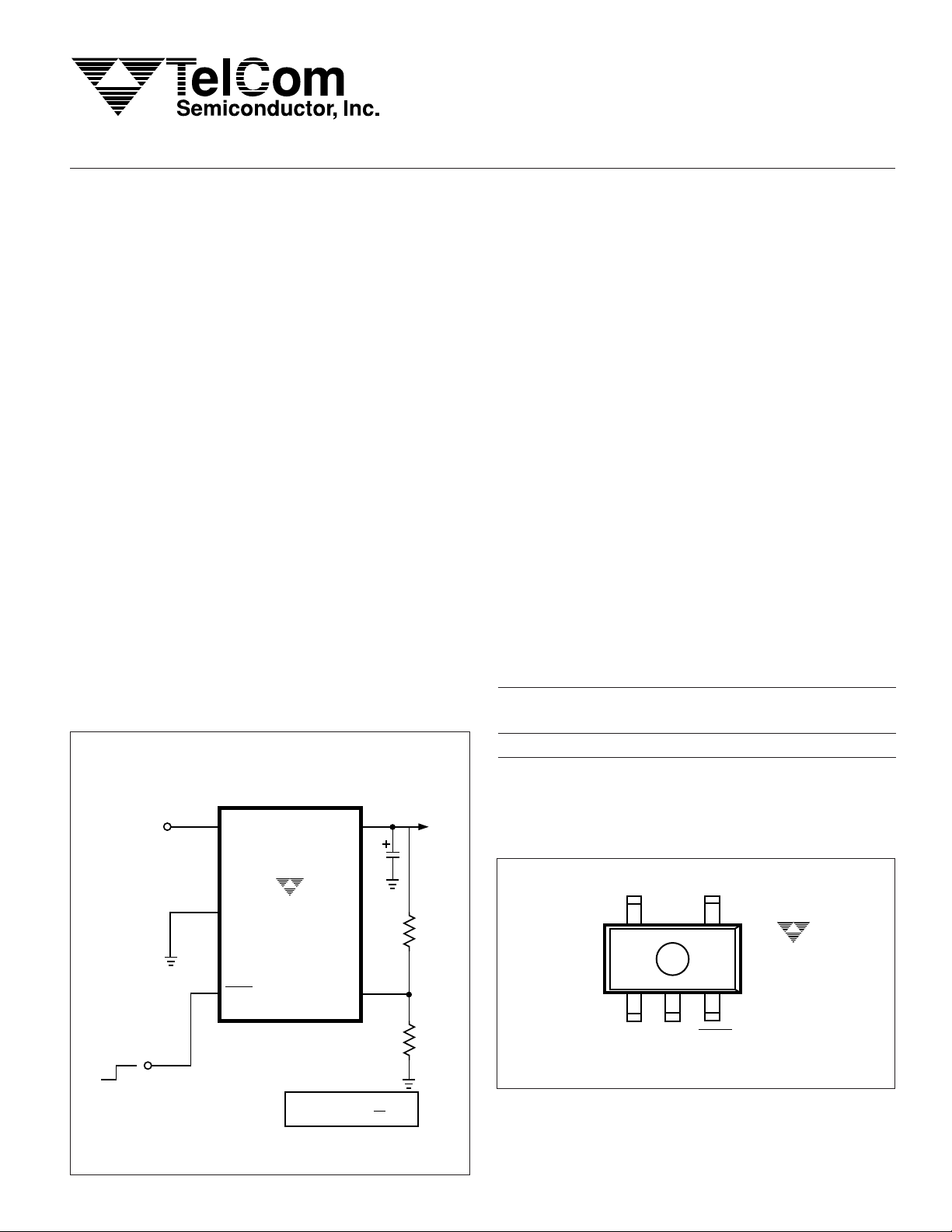
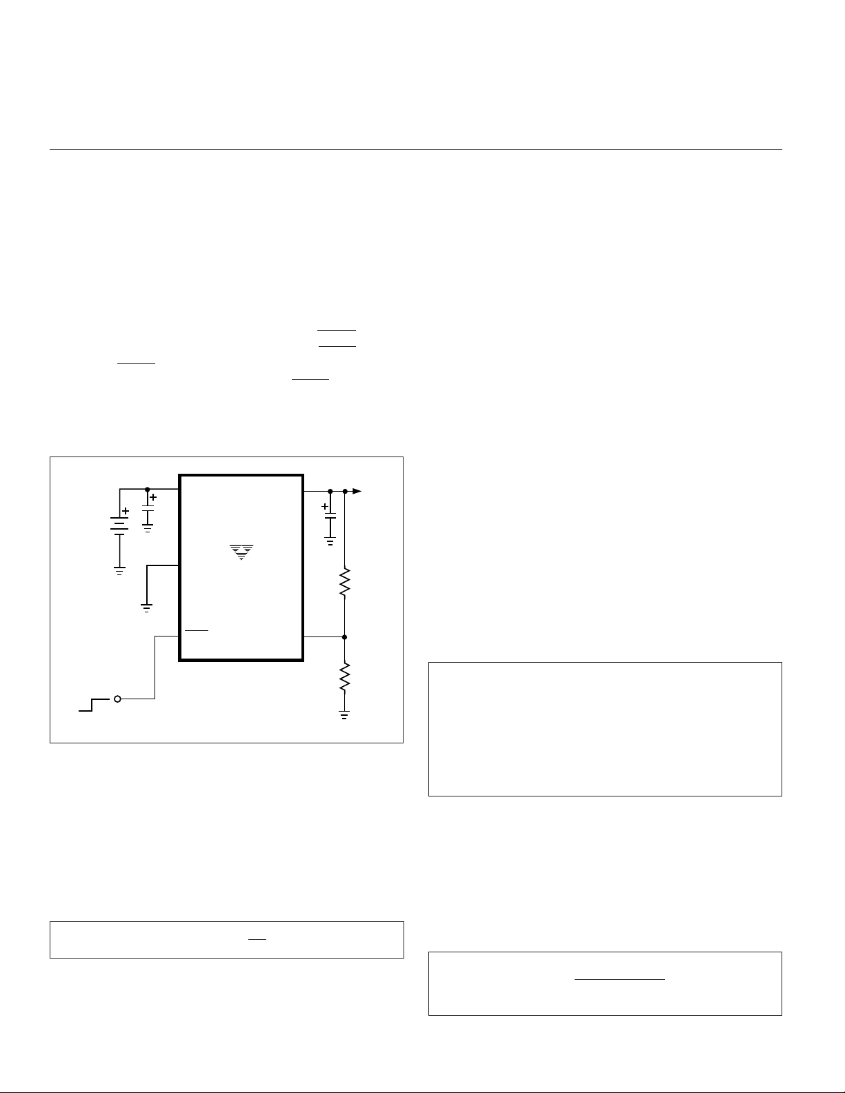
TYPICAL APPLICATION
V
IN
1
3
2
V
IN
GND
SHDN
TC1070
V
OUT
ADJ
5
C1
1µF
R1
4
R2
GENERAL DESCRIPTION
The TC1070 is an adjustable LDO designed to supercede a variety of older (bipolar) voltage regulators. Designed specifically for battery-operated systems, the
TC1070’s CMOS construction eliminates wasted ground
current, significantly extending battery life. Total supply
current is typically 50µA at full load (
than in bipolar regulators
!).
20 to 60 times lower
TC1070 key features include ultra low noise operation
very low dropout voltage (typically 100mV at full load) and
internal feed-forward compensation for fast response to
step changes in load. Supply current is reduced to less than
1µA when the shutdown input is low. The TC1070 incorporates both over-temperature and over-current protection.
Output voltage is programmed with a simple resistor divider
from V
OUT
to ADJ.
The TC1070 is stable with an output capacitor of only
1µF and has a maximum output current of 50mA. For higher
output versions, please see the TC1107, TC1108
(I
= 300mA) data sheets.
OUT
ORDERING INFORMATION
Output Junction
Part No. Voltage **(V) Package Temp. Range
TC1070VCT Adjustable SOT-23A-5* – 40°C to +125°C
NOTE: *SOT-23A-5 is equivalent to the EIAJ (SC-74A)
** Other output voltages available. Please contact TelCom
Semiconductor for details
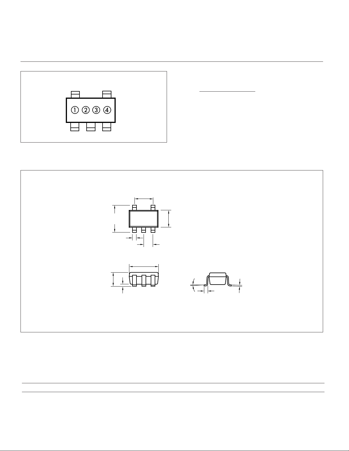
V
OUT
PIN CONFIGURATION
V
OUT
5
1
V
IN
2
GND
ADJ
4
3
SHDN
TC1070
(SOT-23A-5*)
TOP VIEW
Shutdown Control
(from Power Control Logic)
TC1070-01 6/13/97
TelCom Semiconductor reserves the right to make changes in the circuitry and specifications ot its devices.
= V
REF
x [R2
V
OUT
R1
+ 1
NOTE: *SOT-23A-5 is equivalent to the EIAJ (SC-74A)
]
1
Page 2
PRELIMINARY INFORMATION
TC1070
ABSOLUTE MAXIMUM RATINGS*
Input Voltage .................................................................7V
Output Voltage .................................. (– 0.3) to (VIN + 0.3)
Power Dissipation .................... Internally Limited (Note 7)
Operating Temperature.................... – 40°C < TJ < 125°C
Storage Temperature ............................– 65°C to +150°C
Maximum Voltage on Any Pin ........... VIN + 0.3V to – 0.3V
Lead Temperature (Soldering, 10 Sec.)................+260°C
50mA ADJUSTABLE CMOS
LDO WITH SHUTDOWN
*Stresses beyond those listed under "Absolute Maximum Ratings" may
cause permanent damage to the device. These are stress ratings only, and
functional operation of the device at these or any other conditions beyond
those indicated in the operational sections of the specifications is not
implied. Exposure to absolute maximum rating conditions for extended
periods may affect device reliability.
ELECTRICAL CHARACTERISTICS: V
IN
= V
+ 1V, IL = 0.1mA, CL = 3.3µF, SHDN > VIH, T
OUT
= 25°C, unless other-
A
wise specified. BOLDFACE type specifications apply for junction temperatures of
– 40°C to +125°C.
Symbol Parameter Test Conditions Min Typ Max Units
V
IN
I
OUT
MAX
V
OUT
V
REF
∆V
/∆TV
REF
∆V
/∆V
OUT
∆V
OUT/VOUT
V
– V
IN
OUT
I
GND
I
IN
I
INSD
PSRR Power Supply Rejection Ratio F
I
OUT
SC
∆V
/∆P
OUT
T
SD
∆T
SD
eN Output Noise IL = I
Input Operating Voltage — — 6.5 V
Maximum Output Current 50 —— mA
Output Voltage V
I
REF
= 0
L
≤ V
≤ (VIN –0.05) VR – 2.5% VR ±0.5% VR + 2.5% V
OUT
(Note 1)
Reference Voltage
Temperature Coefficient Note 2 — 40 — ppm/°C
REF
Line Regulation (VR + 1V) < VIN < 6V — 0.05 — %/V
IN
Load Regulation IL = 0.1mA to I
OUT
MAX
—
— 0.5 — %
1.23 — V
(Note 3)
Dropout Voltage (Note 4) IL = 0.1mA — 5 — mV
= 20mA 65
I
L
I
= 50mA 95
L
(Note 4)
Ground Pin Current IL = I
OUT
MAX,
(Note 5)
— 0 — µA
Supply Current SHDN = VIH, IL = 0 — 50 — µA
Shutdown Supply Current SHDN = 0V — — 0.05 µA
≤ 1kHz — 64 — dB
RE
Output Short Circuit Current V
Thermal Regulation Note 6 — 0.04 — %/W
D
Thermal Shutdown Die Temperature
= 0V — 200 450 mA
OUT
— 160 — °C
Thermal Shutdown Hysteresis — 10 — °C
OUT
MAX
— 260 — nV/√Hz
470pF from Bypass to GND
SHDN Input
V
IH
V
IL
SHDN Input High Threshold VIN = 2.5V to 6.5V 45 — — %V
SHDN Input Low Threshold VIN = 2.5V to 6.5V — — 15 %V
IN
IN
TC1070-01 6/13/97
2
Page 3
50mA ADJUSTABLE CMOS
LDO WITH SHUTDOWN
PRELIMINARY INFORMATION
TC1070
ELECTRICAL CHARACTERISTICS:
V
IN
= V
+ 1V, IL = 0.1mA, CL = 3.3µF, SHDN > VIH, T
OUT
= 25°C, unless otherwise noted.
A
Symbol Parameter Test Conditions Min Typ Max Units
ADJ Input
I
ADJ
NOTES: 1. VR is the regulator output voltage setting.
2. TC V
3. Regulation is measured at a constant junction temperature using low duty cycle pulse testing. Load regulation is tested over a load
4. Dropout voltage is defined as the input to output differential at which the output voltage drops 2% below its nominal value.
5. Ground pin current is the regulator pass transistor gate current. The total current drawn from the input supply is the sum of the load
6. Thermal Regulation is defined as the change in output voltage at a time T after a change in power dissipation is applied, excluding load
7. The maximum allowable power dissipation is a function of ambient temperature, the maximum allowable junction temperature and the
Adjust Input Leakage Current — 50 — pA
= (V
OUT
range from 0.1mA to the maximum specified output current. Changes in output voltage due to heating effects are covered by the
thermal regulation specification.
current, ground current and supply current (i.e. IIN = I
or line regulation effects. Specifications are for a current pulse equal to I
thermal resistance from junction-to-air (i.e. TA, TJ, qJA). Exceeding the maximum allowable power dissipation causes the device to
initiate thermal shutdown. Please see
OUT
V
MAX –
OUT
V
OUT
x ∆T
MIN)
6
x 10
Thermal Considerations
SUPPLY
+ I
+ I
GND
section of this data sheet for more details.
).
LOAD
at VIN = 6V for T = 10msec.
LMAX
PIN DESCRIPTION
Pin No.
(SOT-23A-5) Symbol Description
1VINUnregulated supply input.
2 GND Ground terminal.
3 SHDN Shutdown control input. The regulator is fully enabled when a logic high is applied to this
input. The regulator enters shutdown when a logic low is applied to this input. During
shutdown, output voltage falls to zero and supply current is reduced to 0.05 microamp
(typical).
4 ADJ Output voltage adjust terminal. Output voltage setting is programmed with a resistor divider
5V
OUT
from V
(See Text).
Regulated voltage output.
to this input. A capacitor may also be added to this input to resuce output noise
OUT
TC1070-01 6/13/97
3
Page 4
PRELIMINARY INFORMATION
TC1070
50mA ADJUSTABLE CMOS
LDO WITH SHUTDOWN
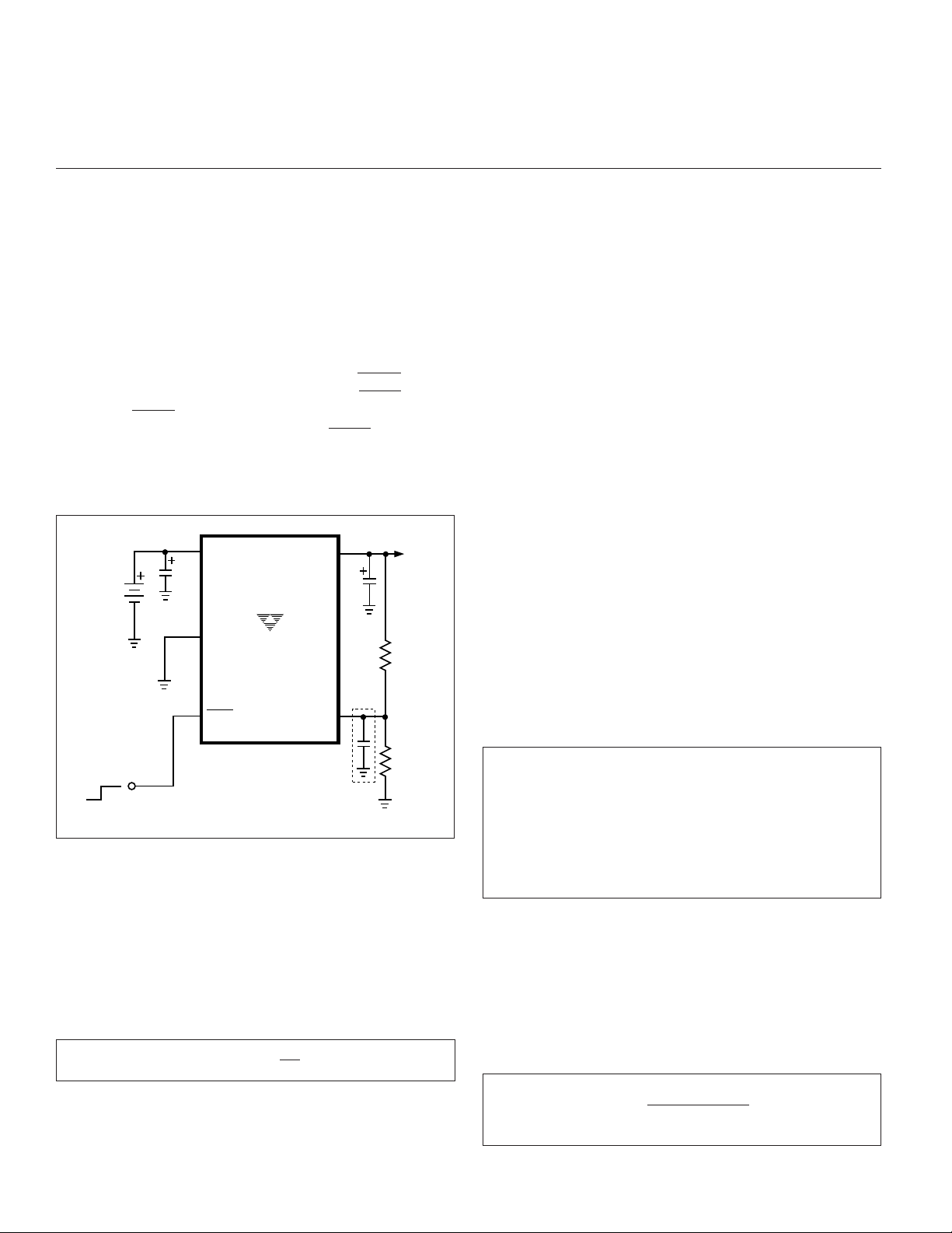
DETAILED DESCRIPTION
The TC1070 is a precision fixed output voltage regulator. (If a fixed version is desired, please see the TC1014 or
TC1015 data sheets.) Unlike the bipolar regulators, the
TC1070 supply current does not increase with load current.
In addition, V
remains stable and within regulation at
OUT
very low load currents (an important consideration in RTC
and CMOS RAM battery back-up applications).
Figure 1 shows a typical application circuit. The regulator is enabled any time the shutdown input (SHDN) is at or
above VIH, and shutdown (disabled) when SHDN is at or
below VIL. SHDN may be controlled by a CMOS logic gate,
or I/O port of a microcontroller. If the SHDN input is not
required, it should be connected directly to the input supply.
While in shutdown, supply current decreases to 0.05µA
(typical) and V
3.0V
BATTERY
Shutdown Control
(from Power Control Logic)
falls to zero volts.
OUT
1
V
IN
C1
1µF
2
GND
TC1070
3
SHDN
Figure 1. 2.45 Battery-Operated Supply
V
OUT
ADJ
C3
100pF
0.01µF
(Optional)
5
C2
1µF
4
R1
2.2M
R2
2.2M
+2.45V
Adjust Input
The output voltage setting is determined by the values
of R1 and R2 (Figure 1). The ohmic values of these resistors
should be between 470K and 3M to minimize bleeder
current.
The output voltage setting is calculated using the following equation.
V
= V
OUT
The voltage adjustment range of the TC1070 is from
V
to (VIN – 0.05V). If so desired, a small capacitor (100pF
REF
to 0.01µF) may be added to the ADJ input to further reduce
output noise.
TC1070-01 6/13/97
[R1
x
REF
R2
Equation 1.
+ 1
]
Output Capacitor
A 1µF (min) capacitor from V
mended. The output capacitor should have an effective
series resistance of 5Ω or less, and a resonant frequency
above 1MHz. A 1µF capacitor should be connected from V
to GND if there is more than 10 inches of wire between the
regulator and the AC filter capacitor, or if a battery is used as
the power source. Aluminum electrolytic or tantalum capacitor types can be used. (Since many aluminum electrolytic
capacitors freeze at approximately – 30°C, solid tantalums
are recommended for applications operating below – 25°C.)
When operating from sources other than batteries, supplynoise rejection and transient response can be improved by
increasing the value of the input and output capacitors and
employing passive filtering techniques.
to ground is recom-
OUT
Thermal Considerations
Thermal Shutdown
Integrated thermal protection circuitry shuts the regulator off when die temperature exceeds 160°C. The regulator
remains off until the die temperature drops to approximately
150°C.
Power Dissipation
The amount of power the regulator dissipates is primarily a function of input and output voltage, and output current.
The following equation is used to calculate worst case
actual
power dissipation:
P
D ≈ (VIN
Where:
PD= Worst case actual power dissipation
V
V
OUT
I
LOAD
The maximum
= Maximum voltage on V
IN
MAX
= Minimum regulator output voltage
MIN
= Maximum output (load) current
MAX
allowable
is a function of the maximum ambient temperature (T
the maximum allowable die temperature (125°C) and the
thermal resistance from junction-to-air (θJA). SOT-23A-5
packag has a θJA of approximately
mounted on a single layer FR4 dielectric copper clad PC
board.
P
D
MAX
θ
Where all terms are previously defined.
4
MAX
Equation 2.
(T
=
Equation 3.
–
V
OUT
MIN
I
)
IN
LOAD
MAX
power dissipation (Equation 2)
220°C/Watt
– T
J
J
MAX
JA
MAX
)
A
MAX
when
IN
),
Page 5

50mA ADJUSTABLE CMOS
LDO WITH SHUTDOWN
Equation 2 can be used in conjunction with Equation 3
to ensure regulator thermal operation is within limits. For
example:
Given:
V
V
OUT
I
T
Find: 1. Actual power dissipation
2. Maximum allowable dissipation
Actual power dissipation:
IN
MAX
LOAD
AMAX
MIN
= 3.0V ±10%
= 2.7V ±0.5V
= 40mA
= 55°C
PRELIMINARY INFORMATION
TC1070
P
D ≈ (VIN
= [(3.0 x 1.05) – (2.7 x .995)]40 x 10
MAX
–
V
OUT
MIN
I
LOAD
)
MAX
–3
= 18.5mW
Maximum allowable power dissipation:
P
θ
D
MAX
= (T
J
MAX
– T
JA
A
MAX
)
= (125 – 55)
220
= 318mW
In this example, the TC1070 dissipates a maximum of
only 60mW; far below the allowable limit of 318mW. In a
similar manner, Equation 2 and Equation 3 can be used to
calculate maximum current and/or input voltage limits.
Layout Considerations
The primary path of heat conduction out of the package
is via the package leads. Therefore, layouts having a ground
plane, wide traces at the pads, and wide power supply bus
lines combine to lower θJA and therefore increase the
maximum allowable power dissipation limit.
TC1070-01 6/13/97
5
Page 6
PRELIMINARY INFORMATION
TC1070
50mA ADJUSTABLE CMOS
LDO WITH SHUTDOWN
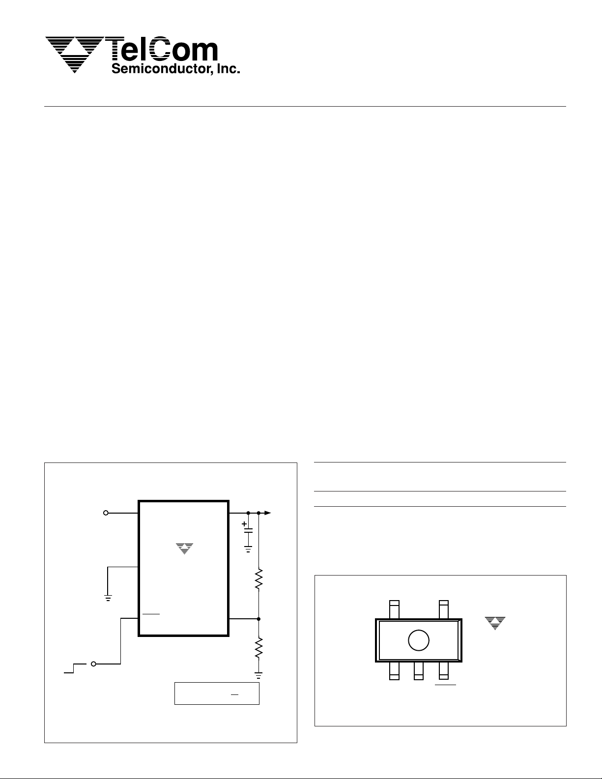
SOT-23A-5
PACKAGE DIMENSIONS
.122 (3.10)
.098 (2.50)
.020 (0.50)
.012 (0.30)
a & b = part number code + temperature range and voltage
TC1070 (V) Code
Adjustable BA
c represents year and quarter code
d represents lot ID number
SOT-23A-5*
.071 (1.80)
.059 (1.50)
.037 (0.95)
REFERENCE
.122 (3.10)
.106 (2.70)
.057 (1.45)
.035 (0.90)
.006 (0.15)
.000 (0.00)
NOTE: *SOT-23A-5 is equivalent to the EIAJ (SC-74A)
Sales Offices
TelCom Semiconductor
1300 Terra Bella Avenue
P.O. Box 7267
Mountain View, CA 94039-7267
TEL: 415-968-9241
FAX: 415-967-1590
E-Mail: liter@c2smtp.telcom-semi.com
TC1070-01 6/13/97
10° MAX.
.022 (0.55)
.008 (0.20)
TelCom Semiconductor
Austin Product Center
9101 Burnet Rd. Suite 214
Austin, TX 78758
TEL: 512-873-7100
FAX: 512-873-8236 TelCom
6
.010 (0.25)
.004 (0.09)
Dimensions: inches (mm)
TelCom Semiconductor H.K. Ltd.
10 Sam Chuk Street, 6/F
San Po Kong
Kowloon
Hong Kong
TEL: 852-2324-0122
FAX: 852-2354-9957
Printed in the U.S.A.
Page 7
100mA ADJUSTABLE CMOS
PRELIMINARY INFORMATION
LDO WITH SHUTDOWN
100mA ADJUSTABLE CMOS LDO WITH SHUTDOWN
TC1071
TC1071
FEATURES
■ Zero Ground Current for Longer Battery Life!
■ Adjustable Output Voltage
■ Very Low Dropout Voltage
■ Guaranteed 100mA Output
■ Power-Saving Shutdown Mode
■ Over-Current and Over-Temperature Protection
■ Space-Saving SOT-23A-5 Package
■
Pin Compatible with LP2980 and MIC5205 Regulators
APPLICATIONS
■ Battery Operated Systems
■ Portable Computers
■ Medical Instruments
■ Instrumentation
■ Cellular / GSM / PHS Phones
■ Linear Post-Regulator for SMPS
■ Pagers
GENERAL DESCRIPTION
The TC1071 is an adjustable LDO designed to supercede a variety of older (bipolar) voltage regulators. Designed specifically for battery-operated systems, the
TC1070’s CMOS construction eliminates wasted ground
current, significantly extending battery life. Total supply
current is typically 50µA at full load (
than in bipolar regulators
!).
TC1071 key features include ultra low noise operation
very low dropout voltage (typically 200mV at full load) and
internal feed-forward compensation for fast response to
step changes in load. Supply current is reduced to less than
1µA when the shutdown input is low. The TC1071 incorporates both over-temperature and over-current protection.
Output voltage is programmed with a simple resistor divider
from V
OUT
to ADJ.
The TC1071 is stable with an output capacitor of only
1µF and has a maximum output current of 100mA. For
higher output versions, please see the TC1174
(I
= 300mA) data sheet.
OUT
20 to 60 times lower
TYPICAL APPLICATION
V
IN
Shutdown Control
(from Power Control Logic)
1
3
2
V
GND
SHDN
ORDERING INFORMATION
Output Junction
Part No. Voltage **(V) Package Temp. Range
5
V
OUT
= V
REF
OUT
ADJ
x [R2
C1
1µF
4
+ 1
IN
TC1071
V
R1
V
OUT
R1
R2
]
TC1071VCT Adjustable SOT-23A-5* – 40°C to +125°C
NOTE: *SOT-23A-5 is equivalent to the EIAJ (SC-74A)
**Other output voltages available. Please contact TelCom
Semiconductor for details
PIN CONFIGURATION
V
OUT
5
1
V
IN
NOTE: *SOT-23A-5 is equivalent to the EIAJ (SC-74A)
2
GND
ADJ
4
3
SHDN
TC1071
(SOT-23A-5*)
TOP VIEW
TC1071-01 6/13/97
TelCom Semiconductor reserves the right to make changes in the circuitry and specifications ot its devices.
1
Page 8

PRELIMINARY INFORMATION
TC1071
ABSOLUTE MAXIMUM RATINGS*
Input Voltage .................................................................7V
Output Voltage .................................. (– 0.3) to (VIN + 0.3)
Power Dissipation .................... Internally Limited (Note 7)
Operating Temperature.................... – 40°C < TJ < 125°C
Storage Temperature ............................– 65°C to +150°C
Maximum Voltage on Any Pin ........... VIN + 0.3V to – 0.3V
Lead Temperature (Soldering, 10 Sec.)................+260°C
100mA ADJUSTABLE CMOS
LDO WITH SHUTDOWN
*Stresses beyond those listed under "Absolute Maximum Ratings" may
cause permanent damage to the device. These are stress ratings only, and
functional operation of the device at these or any other conditions beyond
those indicated in the operational sections of the specifications is not
implied. Exposure to absolute maximum rating conditions for extended
periods may affect device reliability.
ELECTRICAL CHARACTERISTICS:
VIN = V
+ 1V, IL = 0.1mA, CL = 3.3µF, SHDN > VIH, T
OUT
= 25°C, unless other-
A
wise specified.BOLDFACE type specifications apply for junction temperatures of
– 40°C to +125°C.
Symbol Parameter Test Conditions Min Typ Max Units
V
IN
I
OUT
MAX
V
OUT
V
REF
∆V
/∆TV
REF
∆V
/∆V
OUT
∆V
OUT/VOUT
V
– V
IN
OUT
I
GND
I
IN
I
INSD
PSRR Power Supply Rejection Ratio F
I
OUT
SC
∆V
/∆P
OUT
eN Output Noise IL = I
Input Operating Voltage — — 6.5 V
Maximum Output Current 100 —— mA
Output Voltage V
≤ V
REF
I
= 0
L
≤ (VIN –0.05) VR – 2.5% VR ±0.5% VR + 2.5% V
OUT
(Note 1)
Reference Voltage
Temperature Coefficient Note 2 — 40 —
REF
Line Regulation (VR + 1V) < VIN < 6V — 0.05 — %/V
IN
Load Regulation IL = 0.1mA to I
OUT
MAX
—
— 0.5 — %
1.23 — V
(Note 3)
Dropout Voltage (Note 4) IL = 0.1mA — 20 — mV
I
= 20mA 70
L
= 50mA 93
I
L
= 100mA 112
I
L
(Note 4)
Ground Pin Current IL = I
OUT
MAX,
(Note 5)
— 0 — µA
Supply Current SHDN = VIH, IL = 0 — 50 — µA
Shutdown Supply Current SHDN = 0V — — 0.05 µA
≤ 1kHz — 64 — dB
RE
Output Short Circuit Current V
Thermal Regulation Note 6 — 0.04 — %/W
D
= 0V — 300 450 mA
OUT
OUT
MAX
— 260 — nV/√Hz
470pF from Bypass to GND
SHDN Input
V
IH
V
IL
SHDN Input High Threshold VIN = 2.5V to 6.5V 45 — — %V
SHDN Input Low Threshold VIN = 2.5V to 6.5V — — 15 %V
IN
IN
TC1071-01 6/13/97
2
Page 9
100mA ADJUSTABLE CMOS
LDO WITH SHUTDOWN
PRELIMINARY INFORMATION
TC1071
ELECTRICAL CHARACTERISTICS:
V
IN
= V
+ 1V, IL = 0.1mA, CL = 3.3µF, SHDN > VIH, T
OUT
= 25°C, unless otherwise noted.
A
Symbol Parameter Test Conditions Min Typ Max Units
ADJ Input
I
ADJ
NOTES: 1. VR is the regulator output voltage setting.
2. TC V
3. Regulation is measured at a constant junction temperature using low duty cycle pulse testing. Load regulation is tested over a load
4. Dropout voltage is defined as the input to output differential at which the output voltage drops 2% below its nominal value.
5. Ground pin current is the regulator pass transistor gate current. The total current drawn from the input supply is the sum of the load
6. Thermal Regulation is defined as the change in output voltage at a time T after a change in power dissipation is applied, excluding load
7. The maximum allowable power dissipation is a function of ambient temperature, the maximum allowable junction temperature and the
Adjust Input Leakage Current — 50 — pA
= (V
OUT
range from 0.1mA to the maximum specified output current. Changes in output voltage due to heating effects are covered by the
thermal regulation specification.
current, ground current and supply current (i.e. IIN = I
or line regulation effects. Specifications are for a current pulse equal to I
thermal resistance from junction-to-air (i.e. TA, TJ, qJA). Exceeding the maximum allowable power dissipation causes the device to
initiate thermal shutdown. Please see
OUT
V
MAX –
OUT
V
OUT
x ∆T
MIN)
6
x 10
Thermal Considerations
SUPPLY
+ I
+ I
GND
section of this data sheet for more details.
).
LOAD
at VIN = 6V for T = 10msec.
LMAX
PIN DESCRIPTION
Pin No.
(SOT-23A-5) Symbol Description
1VINUnregulated supply input.
2 GND Ground terminal.
3 SHDN Shutdown control input. The regulator is fully enabled when a logic high is applied to this
input. The regulator enters shutdown when a logic low is applied to this input. During
shutdown, output voltage falls to zero and supply current is reduced to 0.05 microamp
(typical).
4 ADJ Output voltage adjust terminal. Output voltage setting is programmed with a resistor divider
to this input. A capacitor may also be added to this input to resuce output noise
OUT
5V
OUT
from V
(See Text).
Regulated voltage output.
TC1071-01 6/13/97
3
Page 10
PRELIMINARY INFORMATION
TC1071
100mA ADJUSTABLE CMOS
LDO WITH SHUTDOWN
DETAILED DESCRIPTION
The TC1071 is a precision fixed output voltage regulator. (If a fixed version is desired, please see the TC1014 or
TC1015 data sheets.) Unlike the bipolar regulators, the
TC1071 supply current does not increase with load current.
In addition, V
very low load currents (an important consideration in RTC
and CMOS RAM battery back-up applications).
Figure 1 shows a typical application circuit. The regulator is enabled any time the shutdown input (SHDN) is at or
above VIH, and shutdown (disabled) when SHDN is at or
below VIL. SHDN may be controlled by a CMOS logic gate,
or I/O port of a microcontroller. If the SHDN input is not
required, it should be connected directly to the input supply.
While in shutdown, supply current decreases to 0.05µA
(typical) and V
3.0V
BATTERY
remains stable and within regulation at
OUT
falls to zero volts.
OUT
C1
1µF
1
3
2
V
IN
GND
SHDN
TC1071
V
OUT
ADJ
5
C2
1µF
4
R1
2.2M
R2
2.2M
+2.45V
Output Capacitor
A 1µF (min) capacitor from V
mended. The output capacitor should have an effective
series resistance of 5Ω or less, and a resonant frequency
above 1MHz. A 1µF capacitor should be connected from V
to GND if there is more than 10 inches of wire between the
regulator and the AC filter capacitor, or if a battery is used as
the power source. Aluminum electrolytic or tantalum capacitor types can be used. (Since many aluminum electrolytic
capacitors freeze at approximately – 30°C, solid tantalums
are recommended for applications operating below – 25°C.)
When operating from sources other than batteries, supplynoise rejection and transient response can be improved by
increasing the value of the input and output capacitors and
employing passive filtering techniques.
to ground is recom-
OUT
Thermal Considerations
Thermal Shutdown
Integrated thermal protection circuitry shuts the regulator off when die temperature exceeds 160°C. The regulator
remains off until the die temperature drops to approximately
150°C.
Power Dissipation
The amount of power the regulator dissipates is primarily a function of input and output voltage, and output current.
The following equation is used to calculate worst case
actual
power dissipation:
P
D ≈ (VIN
MAX
–
V
OUT
MIN
I
)
LOAD
MAX
IN
Shutdown Control
(from Power Control Logic)
Figure 1. 2.45 Battery-Operated Supply
Adjust Input
The output voltage setting is determined by the values
of R1 and R2 (Figure 1). The ohmic values of these resistors
should be between 470K and 3M to minimize bleeder
current.
The output voltage setting is calculated using the following equation.
V
= V
OUT
The voltage adjustment range of the TC1071 is from
V
to (VIN – 0.05V). If so desired, a small capacitor (100pF
REF
to 0.01µF) may be added to the ADJ input to further reduce
output noise.
TC1071-01 6/13/97
[R1
x
REF
R2
Equation 1.
+ 1
]
Where:
PD= Worst case actual power dissipation
V
V
OUT
I
LOAD
The maximum
= Maximum voltage on V
IN
MAX
= Minimum regulator output voltage
MIN
= Maximum output (load) current
MAX
Equation 2.
allowable
power dissipation (Equation 3)
IN
is a function of the maximum ambient temperature (T
the maximum allowable die temperature (125°C) and the
thermal resistance from junction-to-air (θJA). SOT-23A-5
package has a θJA of approximately
220°C/Watt
mounted on a single layer FR4 dielectric copper clad PC
board.
P
D
(T
J
=
MAX
MAX
θ
– T
JA
A
MAX
)
Where all terms are previously defined.
Equation 3.
4
A
MAX
when
),
Page 11

100mA ADJUSTABLE CMOS
LDO WITH SHUTDOWN
Equation 2 can be used in conjunction with Equation 3
to ensure regulator thermal operation is within limits. For
example:
Given:
V
V
OUT
I
T
Find: 1. Actual power dissipation
2. Maximum allowable dissipation
Actual power dissipation:
IN
MAX
LOAD
AMAX
MIN
= 3.0V ±10%
= 2.7V ±0.5V
= 98mA
= 55°C
PRELIMINARY INFORMATION
TC1071
P
D ≈ (VIN
= [(3.0 x 1.1) – (2.7 x .995)]40 x 10
MAX
–
V
OUT
MIN
I
LOAD
)
MAX
–3
= 60mW
Maximum allowable power dissipation:
P
θ
D
MAX
= (T
J
MAX
JA
– T
A
MAX
)
= (125 – 55)
220
= 318mW
In this example, the TC1071 dissipates a maximum of
only 60mW; far below the allowable limit of 318mW. In a
similar manner, Equation 1 and Equation 2 can be used to
calculate maximum current and/or input voltage limits. For
example, the maximum allowable VIN is found by substituting the maximum allowable power dissipation of 318mW
into Equation 1, from which V
IN
MAX
= 5.9V.
Layout Considerations
The primary path of heat conduction out of the package
is via the package leads. Therefore, layouts having a ground
plane, wide traces at the pads, and wide power supply bus
lines combine to lower θJA and therefore increase the
maximum allowable power dissipation limit.
TC1071-01 6/13/97
5
Page 12

PRELIMINARY INFORMATION
TC1071
100mA ADJUSTABLE CMOS
LDO WITH SHUTDOWN
SOT-23A-5
PACKAGE DIMENSIONS
.122 (3.10)
.098 (2.50)
a & b = part number code + temperature range and voltage
TC1071 (V) Code
Adjustable BB
c represents year and quarter code
d represents lot ID number
SOT-23A-5*
.071 (1.80)
.059 (1.50)
.020 (0.50)
.012 (0.30)
.057 (1.45)
.035 (0.90)
.006 (0.15)
.000 (0.00)
NOTE: *SOT-23A-5 is equivalent to the EIAJ (SC-74A)
Sales Offices
TelCom Semiconductor
1300 Terra Bella Avenue
P.O. Box 7267
Mountain View, CA 94039-7267
TEL: 415-968-9241
FAX: 415-967-1590
E-Mail: liter@c2smtp.telcom-semi.com
.037 (0.95)
REFERENCE
.122 (3.10)
.106 (2.70)
10° MAX.
TelCom Semiconductor
Austin Product Center
9101 Burnet Rd. Suite 214
Austin, TX 78758
TEL: 512-873-7100
FAX: 512-873-8236 TelCom
.010 (0.25)
.004 (0.09)
.022 (0.55)
.008 (0.20)
Dimensions: inches (mm)
TelCom Semiconductor H.K. Ltd.
10 Sam Chuk Street, 6/F
San Po Kong
Kowloon
Hong Kong
TEL: 852-2324-0122
FAX: 852-2354-9957
TC1071-01 6/13/97
6
Printed in the U.S.A.
 Loading...