

Page 1
UA
SOP
TC1040
Linear Building Block – Dual Low Power Comparator and
Voltage Reference with Shutdown
Features
• Combines Two Comparators and a Voltage
Reference in a Single Package
• Optimized for SingleSupply Operation
• Small Package: 8-Pin MSOP
• Ultra Low Input Bias Current: Less than100pA
• Low Quiescent Current, Operating: 10µA(Typ.)
Shutdown Mode: 6µA(Typ.)
• Rail-to-Rail Inputs and Outputs
•OperatesDowntoV
DD
=1.8V
• Referenceand One Comparator Remain Active in
Shutdown to Provide Supervisory Functions
Applications
• Power Supply Circuits
• Battery Operated Equipment
• Consumer Products
• Replacements for Discrete Components
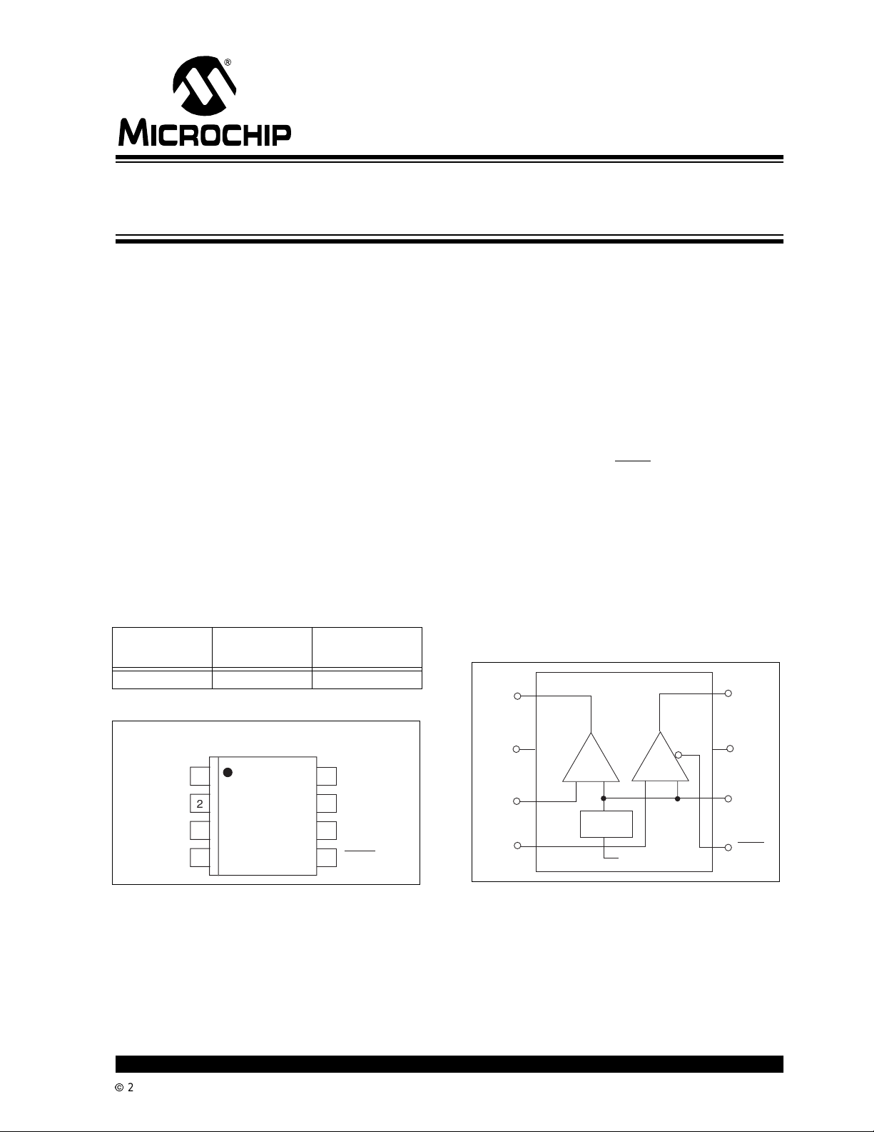
Device Selection Table
Part Number Package
TC1040CEUA 8-Pin MSOP -40°C to +85°C
Temperature
Range
Package Type
General Description
The TC1040 is a mixed-function device combining two
comparators and a voltage reference in a single 8-pin
package. The inverting input of Comparator A and the
non-inverting input of Comparator B are internally
connected to thereference.
This increased integration allows the user to replace
two packages, which saves space, lowers supply
current and increases system performance. The
TC1040 operates from two 1.5V alkaline cells down to
V
= 1.8V. It requires only 10µA typical of supply
DD
current, which significantly extends battery life. A low
power shutdown input (SHDN
) disables one of the
comparators, placing its outputs in a high-impedance
state. This mode saves battery power and allows
comparator outputs to share common analog lines
(multiplexing). Shutdown current is 6µA(typical).
Rail-to-rail inputs and outputs allow operation from low
supply voltages with large input and output signal
swings.
Packaged in an 8-Pin MSOP, the TC1040 is ideal for
applicationsrequiring low power leveldetection.
Functional Block Diagram
OUTA
1
TC1040
8
OUTB
-Pin M
OUTB
OUTA
V
SS
INA+
INB-
2002 Microchip TechnologyInc. DS21345B-page 1
TC1040CE
8
7
6
5
V
DD
REF
SHDN
V
INA+
INB-
2
SS
3
4
A
+
–
Voltage
Reference
B
–
V
SS
7
V
DD
+
6
REF
5
SHDN
Page 2

TC1040
1.0 ELECTRICAL
CHARACTERISTICS
*Stresses above those listed under "Absolute Maximum
Ratings" may cause permanent damage to the device. These
are stress ratings only and functional operation of t he device
at these or any other conditions above those indicated in the
ABSOLUTE MAXIMUM RATINGS*
Supply Voltage......................................................6.0V
Voltage on Any Pin..........(V
– 0.3V) to (VDD+0.3V)
SS
operation sections of the specifications is not implied.
Exposure to Absolute Maximum Rating conditions for
extended periods may affectdevice reliability.
Junction Temperature.......................................+150°C
Operating Temperature Range.............-40°C to +85°C
StorageTemperature Range..............-55°C to +150°C
TC1040 ELECTRICAL SPECIFICATIONS
Electrical Characteristics: Typical values apply at 25°C and VDD= 3.0V. Minimum and maximum values apply for TA= -40° to
+85°C and V
Symbol Parameter Min Typ Max Units Test Conditions
V
DD
I
Q
I
SHDN
Shutdown Input
V
IH
V
IL
I
SI
Comparators
(SD) Output Resistance in Shutdown 20 — — MΩ SHDN =VSS,COMPBonly
R
OUT
(SD) Output Capacitance in Sh utdown — — 5 pF SHDN =VSS,COMPBonly
C
OUT
T
SEL
T
DESEL
V
IR
V
OS
I
B
V
OH
V
OL
PSRR Power Supply Rejection Ratio 60 — — dB TA=25°C
I
SRC
I
SINK
t
PD1
t
PD2
Voltage Reference
V
REF
I
REF(SOURCE)
I
REF(SINK)
C
L(REF)
E
VREF
e
VREF
= 1.8V to 5.5V,unless otherwise specified.
DD
Supply Voltage 1.8 — 5.5 V
SupplyCurrent Operating — 10 15 µA All outputs unloaded, SHDN =V
Supply Current, Shutdown — 0.05 0.1 µA SHDN =V
InputHighThreshold 80% V
Input Low Threshold — — 20% V
——V
DD
DD
V
SS
Shutdown Input Current — — ±100 nA
Select Time (For Valid Output) — 20 — µsec (SHDN =VIHto V
R
=10kΩ to V
L
Deselect Time — 500 — nsec (SHDN =VILto V
R
=10kΩ to V
L
)
OUT
COMPB only
SS,
)
OUT
COMPB only
SS,
Input Voltage Range VSS–0.2 — VDD+0.2 V
Input Offset Voltage -5
-5
—+5+5mV VDD=3V,TA=25°C
T
=-40°Cto85°C
A
Input Bias Current — — ±100 pA TA= 25°C, INA+, INB-= VDDto V
OutputHighVoltage VDD–0.3 — — V RL=10kΩ to V
OutputLow Voltage — — 0.3 V RL=10kΩ to V
V
=1.8Vto5V
DD
OutputSource Current 1 — — mA INA+= VDD,INB-=V
OutputShorted to V
SS
DD
SS
SS
VDD=1.8V
OutputSinkCurrent 2 — — mA INA+= VSS,INB-=V
OutputShorted to V
VDD=1.8V
DD,
DD
Response Time — 4 — µsec 100mV Overdrive, CL= 100pF
Response Time — 6 — µsec 10mV Overdrive,CL= 100pF
Reference Voltage 1.176 1.200 1.224 V
Source Current 50 — — µA
Sink Current 50 — — µA
Load Capacitance — — 100 pF
Voltage Noise — 20 — µV
100Hz to 100kHz
RMS
Noise Density — 1.0 — µV/√Hz 1kHz
DD
SS
DS21345B-page 2
2002 Microchip TechnologyInc.
Page 3
2.0 PIN DESCRIPTION
The description of the pins are listed i n Table 2-1.
TABLE 2-1: P IN FUNCTION TABLE
TC1040
Pin No.
(8-Pin MSOP)
1 OUTA Comparator output.
2V
3 INA+ Non-inverting input to Comparator A.
4 INB- InvertinginputtoComparator B.
5 SHDN
6 REF Voltage reference output.
7V
8 OUTB Comparator output.
Symbol Description
SS
DD
Negative power supply.
Shutdown input.
Positive power supply.
2002 Microchip TechnologyInc. DS21345B-page 3
Page 4
TC1040
3.0 DETAILED DESCRIPTION
The TC1040 i s oneof a series of v ery lowpower, linear
building block products targeted at low voltage, single
supply applications. The TC1040 minimum operating
voltage is 1.8V and typical supply current is only 10µA
(fully enabled). It combines two comparators and a
voltage reference in a single package. A shutdown
mode is incorporated for easy adaptation to system
power management schemes. During shutdown, one
comparatoris disabled (i.e., powered down with output
at a high impedance).The“stillawake”comparatorand
voltage reference can be used as a wake-up timer,
power supply monitor, LDO controller or other
continuous duty circuit function.
3.1 Comparators
The TC1040 contains t wo comparators. The comparator’s inputrange extends beyond both supply voltages
by 200mV and the outputs will swing to within several
millivolts of thesupplies,depending on theload current
being driven. The inverting input of Comparator A and
the non-inverting input of Comparator B are internally
connected to the output of the voltage reference.
The comparators exhibit a propagation delay and
supply current which are largely independent of supply
voltage. The low input bias current and offset voltage
make them suitable f or high impedance precision
applications.
Comparator B is disabled during shutdown and has a
high impedance output. Comparator COMPA remains
active.
3.2 Voltage Reference
A 2.0 percent tolerance, internally biased, 1.20V
bandgap voltage reference is included in the TC1040.
It has a push-pull output capable of sourcing and
sinking 50µA. The voltage reference remains fully
enabled during shutdown.
4.0 TYPICAL APPLICATIONS
The TC1040 lends itself to a wide variety of
applications,particularlyin battery powered systems. It
typically finds application in power management,
processor supervisory and interface circuitry.
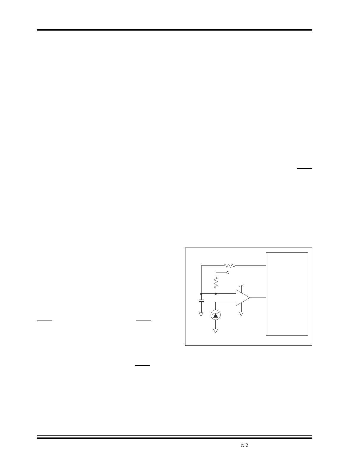
4.1 Wake-Up Timer
Many microcontrollers havea l ow-power “sleep” mode
thatsignificantly reduces their supply current. Typically,
the microcontrolleris placedin thismode via a software
instruction, and returns to a fully-enabled state upon
reception of an external signal (“wake-up”). Thewakeup signal isusually supplied by a hardware timer. Most
system applicationsdemandthatthis timer have along
duration (typically seconds or minutes), and consume
as l ittle supply current aspossible.
The circuit shown in Figure 4-1 is a wake-up timer
made from Comparator A. (Comparator A is used
because the wake-up timer must operate when SHDN
is active.) Capacitor C1 charges through R1 until a
voltage equal to V
“wake-up” is driven active. Upon wake-up, the
microcontroller resets the timer by forcing a logic low
on a dedicated,opendrainI/Oportpin. Thisdischarges
C1 through R4 (the value of R4 is chosen to limit
maximum current sunk by the I/O port pin). With a 3V
supply, the circuit as shown consumes typically 8µA
and f urnishes a nominal timer duration of25 seconds.
FIGURE 4-1: WAKE-UP TIMER
R1
5M
C
1
10µF
is reached, at which point the
R
Microcontroller
I/O*
Wake-Up
1/2
R4
V
DD
V
DD
COMPA
+
–
3.3 Shutdown Input
SHDN at VILdisablesonecomparator.TheSHDN input
cannot be allowed to float; whennotused, connect it to
V
. The disabled comparator’s output is in a high
DD
impedance state when shutdown is active. The
disabledcomparator’s inputsandoutputscan bedriven
from rail-to-rail by an external voltage when the
TC1040 is inshutdown.No latchup wi ll occurwhen the
device is driven to its enabled state when SHDN
to V
.
IH
DS21345B-page 4
is set
*Open Drain Port Pin
V
R
TC1040
2002 Microchip TechnologyInc.
Page 5
TC1040
4.2 Precision Battery Monitor
Figure 4-2 is a precision battery low/battery dead
monitoring circuit. Typically, the battery low output
warns the user that a battery dead condition i s
imminent. Battery dead typically initiates a forced
shutdown to prevent operation at low internal supply
voltages(whichcan cause unstable system operation).
The circuit in Figure 4-2 uses a single TC1040, onehalf of a TC1029, and only six external r esistors.
COMPA and COMPB provide precision voltage
detection using V
R4 set the detection threshold for BATT LOW
as a reference. Resistors R2 and
R
, while
Resistors R1 and R7 set the detection threshold for
BATT FAIL. The component values shown assert
BATT LOW
at 2.2V (typical) and BATT FAIL at 2.0
(typical). Total current consumed by this circuit is
typically 22µA at 3V. Resistors R5 and R6 provide
hysteresis for comparators COMPA and COMPB,
respectively.
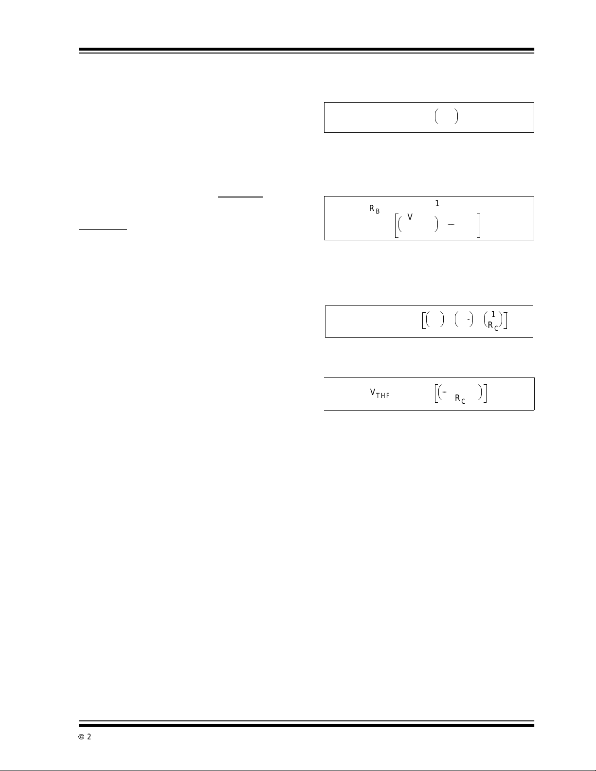
4.3 External Hysteresis (Comparator)
Hysteresis can be set externally with two resistors
using positive f eedback techniques (see Figure4-3).
The design procedure for setting external comparator
hysteresis is as follows:
1. Choose the feedback resistor R
input bias current of the comparator is at most
100pA, the current through R
100nA (i.e., 1000 times the input bias current)
and retain excellent accuracy. The current
through R
R
where VRis a stable reference voltage.
C
at the comparator’s trip point is VR/
C
2. Determinethehysteresisvoltage(V
the upper andlower thresholds.
.Sincethe
C
canbesetto
C
)between
HY
3. Calculate R
as follows:
A
EQUATION 4-1:
V
HY
=
-----------
C
V
DD
SRC
RAR
4. Choose the rising threshold voltage for V
(V
).
THR
5. Calculate R
as follows:
B
EQUATION 4-2:
R
-----------------------------------------------------------=
B
---------------------
VRRA×
6. Verify the threshold voltages with these
formulas:
V
rising:
SRC
V
THR
1
1
1
–
–
-------
-------
R
R
A
C
EQUATION 4-3:
V
V
SRC
THR
falling:
VR()RA()
------R
1
A
1
-------
++=
R
B
1
-------
R
C
EQUATION 4-4:
RAVDD×
V
THFVTHR
--------- ------------- ---
–=
R
C
2002 Microchip TechnologyInc. DS21345B-page 5
Page 6

TC1040
FIGURE 4-2: PRECISION BATTERY MONITOR
3V
Alkaline
+
TC1034
TC1040
V
+
AMP1
–
DD
To System DC/DC
Converter
R2, 330k, 1%
R1, 270k, 1%
V
R
R4, 470k, 1%
R5, 7.5M
V
DD
+
COMPA
–
V
DD
–
COMPB
+
R6, 7.5M
R3, 470k, 1%
BATTLOW
BATTFAIL
FIGURE 4-3: COMPARATOR
EXTERNAL HYSTERESIS
CONFIGURATION
R
C
V
SRC
TC1040
R
A
R
B
V
DD
+
–
COMPA
1/2
V
R
V
OUT
DS21345B-page 6
2002 Microchip TechnologyInc.
Page 7

TC1040
5.0 TYPICAL CHARACTERISTICS
Note: The graphs and tables provided following this noteare astatistical summary based ona limited number of
samples and are provided for informational purposes only. The performance characteristics listed herein
are not tested or guaranteed. In some graphs or tables, the data presented may be outside the specified
operating range ( e.g., outside specified power supplyrange) and therefore outside the warranted range.
Comparator Propagation Delay
vs. Supply Voltage
7
= 25
T
°C
A
= 100pF
C
L
sec)
µ
6
Overdrive = 10mV
5
4
3.5
4 4.5 5 5.5
3
DELAY TO RISING EDGE (
2
1.5
2
Overdrive = 50mV
2.5 3
SUPPLY VOLTAGE (V) SUPPLY VOLTAGE (V)
Comparator Propagation Delay
vs. Temperature
7
Overdrive = 100mV
sec)
µ
6
V
DD
V
5
4
DELAY TO FALLING EDGE (
3
-40°C85°C25°C
TEMPERATURE (°C)
DD
V
DD
V
DD
= 5V
= 4V
= 3V
= 2V
Comparator Propagation Delay
vs. Supply Voltage
7
= 25
T
°C
A
= 100pF
C
L
sec)
µ
6
Overdrive = 10mV
5
4
Overdrive = 50mV
3
DELAY TO FALLING EDGE (
2
1.5
2
Overdrive = 100mV
2.5 3
3.5
4 4.5 5 5.5
Comparator Output Swing
vs. Output Source Current
2.5
= 25
°C
T
A
2.0
(V)
OUT
- V
DD
V
1.5
1.0
.5
V
= 1.8V
DD
0
0
12345 6
I
(mA)
SOURCE
V
V
DD
DD
= 3V
= 5.5V
Comparator Propagation Delay
vs. Temperature
7
Overdrive = 100mV
sec)
µ
6
5
4
DELAY TO RISING EDGE (
3
-40°C85°C25°C
TEMPERATURE (°C)
V
DD
V
DD
V
DD
V
DD
Comparator Output Swing
vs. Output Sink Current
2.5
= 25
T
°C
A
2.0
(V)
1.5
SS
- V
1.0
OUT
V
.5
0
012 345
V
I
SINK
DD
= 1.8V
V
DD
(mA)
V
DD
= 5.5V
= 5V
= 4V
= 2V
= 3V
= 3V
6
Comparator Output Short-Circuit
Current vs. Supply Voltage
60
50
40
30
20
10
Sourcing
0
OUTPUT SHORT-CIRCUIT CURRENT (mA)
0
2002 Microchip TechnologyInc. DS21345B-page 7
T
Sinking
12345 6
SUPPLY VOLTAGE (V)
= 85°C
A
TA = -40°C
TA = 25°C
= -40
A
T
= 85°C
T
A
T
A
C
°
= 25°C
1.240
1.220
1.200
1.180
1.160
REFERENCE VOLTAGE (V)
1.140
Reference Voltage vs.
Load Current
V
V
= 1.8V
DD
V
= 1.8V
DD
0
24
LOAD CURRENT (mA)
DD
= 3V
V
DD
Sinking
Sourcing
V
DD
V
= 3V
DD
6
8
= 5.5V
= 5.5V
4
3
2
1
0
10
0
SUPPLY AND REFERENCE VOLTAGES (V)
Line Transient
Response of V
V
DD
V
REF
100 200
TIME (µsec)
REF
300
400
Page 8

TC1040
T
25
5.0 TYPICAL CHARACTERISTICS (CONTINUED)
Reference Voltage
vs. Supply Voltage
1.25
1.20
1.15
1.10
REFERENCE VOLTAGE (V)
1.05
1
23
SUPPLY VOLTAGE (V)
Supply Current vs. Supply Voltage
12
11
A)
µ
(
10
9
8
SUPPLY CURRENT
7
4
5
6
0123456
SUPPLY VOLTAGE (V)
= 85°C
A
TA = -40°C
=
DS21345B-page 8
2002 Microchip TechnologyInc.
Page 9

6.0 PACKAGING INFORMATION
6.1 Package Marking Information
Package marking data not available at this time.
6.2 Taping Form
Component Taping Orientation for 8-Pin MSOP Devices
PIN 1
TC1040
User Direction of Feed
W
Carrier Tape, Number of Components Per Reel and Reel Size
Package Carrier Width (W) Pitch (P) Part Per Full Reel Reel Size
8-Pin MSOP 12 mm 8 mm 2500 13 in
6.3 Package Dimensions
8-Pin MSOP
.026 (0.65) TYP.
.122 (3.10)
.114 (2.90)
P
Standard Reel Component Orientation
for TR Suffix Device
PIN 1
.122 (3.10)
.114 (2.90)
.197 (5.00)
.189 (4.80)
.043 (1.10)
MAX.
.016 (0.40)
.010 (0.25)
2002 Microchip TechnologyInc. DS21345B-page 9
.006 (0.15)
.002 (0.05)
6° MAX.
.028 (0.70)
.016 (0.40)
Dimensions: inches (mm)
.008 (0.20)
.005 (0.13)
Page 10

TC1040
NOTES:
DS21345B-page 10
2002 Microchip TechnologyInc.
Page 11

TC1040
Sales and Support
Data Sheets
Products supportedby a preliminary DataSheetmayhave an erratasheetdescribing minor operational differences and recommendedworkarounds.To determine if an errata sheetexists for a particulardevice, please contact one of the following:
1. Your local Microchip sales office
2. The Microchip CorporateLiterature Center U.S. FAX: (480)792-7277
3. The Microchip Worldwide Site (www .microchip.com)
Pleasespecify which device, revision of silicon and Data Sheet (includeLiterature #) you are using.
New Customer Notification System
Register on our web site (www.microchip.com/cn)to receivethe most currentinformation on our products.
2002 Microchip Technology Inc. DS21345B-page11
Page 12

TC1040
NOTES:
DS21345B-page12 2002 Microchip Technology Inc.
Page 13

TC1040
Information contained in this publication regarding device
applications and the like is intended through suggestion only
and may be superseded by updates. Itis your responsibility to
ensure that your application meets with your specifications.
No representation or warranty is given and no liability is
assumed by Microchip Technology Incorporated with respect
to the accuracy or use ofsuch information, or infringement of
patents or other intellectual property rights arising from such
use or otherwise. Use of Microchip’s products as critical components in life support systems is not authorized except with
express written approval by Microchip. No licenses are conveyed, implicitly orotherwise, under any intellectual property
rights.
Trademarks
The Microchip name and logo, the Microchip logo, F ilterLab,
K
EELOQ,microID,MPLAB,PIC,PICmicro,PICMASTER,
PICSTART, PRO MATE, SEEVAL and The Embedde d Control
SolutionsCompany areregiste red trademarksof MicrochipTechnologyIncorp or ated in the U.S.A. and other countries .
dsPIC, ECONOMONITOR, FanSense, Fle xRO M , fuzzyLAB,
In-Circuit Serial Programming, ICSP, ICEPIC, microPort,
Migratable Memory, MPASM, MPLIB, MPLINK, MPSIM,
MXDEV, PICC, PICDEM, PICDEM.net, rfPIC, Select Mode
and TotalEndurancearetrademarksofMicrochipTechnology
Incorporated in theU.S.A.
Serialized Quick Turn Programming (SQTP) is a service mark
of Microchip TechnologyIncorporated in t he U.S.A.
All other trademarks mentioned herein are property of their
respective companies.
© 2002, Microchip Technology Incorporated, Printed in the
U.S.A., All Rights Reserved.
Printed on recycled paper.
Microchip received QS-9000 quality system
certification for its worldwide headquarters,
design and wafer fabrication facilities in
Chandler and Tempe, Arizona inJuly 1999
and Mountain View, California inMarch 2002.
The Company’s quality system processes and
procedures are QS-9000 compliant for its
®
PICmicro
devices, Serial EEPROMs, microperipherals,
non-volatile memory and analog products. In
addition, Microchip’s quality system for the
design and manufacture of development
systemsisISO 9001certified.
2002 Microchip TechnologyInc. DS21345B-page 13
8-bit MCUs, KEELOQ®code hopping
Page 14

WORLDWIDE SALES AND SERVICE
AMERICAS
Corporate Office
2355 West Chandler Blvd.
Chandler, AZ 85224-6199
Tel: 480-792-7200 Fax: 480-792-7277
Technical Support: 480-792-7627
Web Address: http://www.microchip.com
Rocky Mountain
2355 West Chandler Blvd.
Chandler, AZ 85224-6199
Tel: 480-792-7966 Fax: 480-792-7456
Atlanta
500 Sugar Mill Road, Suite 200B
Atlanta, GA 30350
Tel: 770-640-0034 Fax: 770-640-0307
Boston
2 Lan Drive, Suite 120
Westford, MA 01886
Tel: 978-692-3848 Fax: 978-692-3821
Chicago
333 Pierce Road, Suite 180
Itasca, IL 60143
Tel: 630-285-0071 Fax: 630-285-0075
Dallas
4570 Westgrove Drive, Suite 160
Addison, TX 75001
Tel: 972-818-7423 Fax: 972-818-2924
Detroit
Tri-Atria Office Building
32255 Northwestern Highway, Suite 190
Farmington Hills, MI 48334
Tel: 248-538-2250 Fax: 248-538-2260
Kokomo
2767 S. Albright Road
Kokomo, Indiana 46902
Tel: 765-864-8360 Fax: 765-864-8387
Los Angeles
18201 Von Karman, Suite 1090
Irvine, CA 92612
Tel: 949-263-1888 Fax: 949-263-1338
New York
150 Motor Parkway, Suite 202
Hauppauge, NY 11788
Tel: 631-273-5305 Fax: 631-273-5335
San Jose
Microchip Technology Inc.
2107 North First Street, Suite 590
San Jose, CA 95131
Tel: 408-436-7950 Fax: 408-436-7955
Toronto
6285 Northam Drive, Suite 108
Mississauga, Ontario L4V 1X5, Canada
Tel: 905-673-0699 Fax: 905-673-6509
ASIA/PACIFIC
Australia
Microchip Technology Australia Pty Ltd
Suite 22, 41Rawson Street
Epping 2121, NSW
Australia
Tel: 61-2-9868-6733 Fax: 61-2-9868-6755
China - Beijing
Microchip Technology Consulting (Shanghai)
Co., Ltd., Beijing Liaison Office
Unit 915
Bei Hai Wan Tai Bldg.
No. 6 Chaoyangmen Beidajie
Beijing, 100027, No. China
Tel: 86-10-85282100 Fax: 86-10-85282104
China - Chengdu
Microchip Technology Consulting (Shanghai)
Co., Ltd., Chengdu Liaison Office
Rm. 2401, 24th Floor,
Ming Xing Financial Tower
No. 88 TIDU Street
Chengdu 610016, China
Tel: 86-28-6766200 Fax: 86-28-6766599
China - Fuzhou
Microchip Technology Consulting (Shanghai)
Co., Ltd., Fuzhou Liaison Office
Unit 28F, World Trade Plaza
No. 71 Wusi Road
Fuzhou 350001, China
Tel: 86-591-7503506 Fax: 86-591-7503521
China - Shanghai
Microchip Technology Consulting (Shanghai)
Co., Ltd.
Room 701, Bldg. B
Far East International Plaza
No. 317 Xian Xia Road
Shanghai, 200051
Tel: 86-21-6275-5700 Fax: 86-21-6275-5060
China - Shenzhen
Microchip Technology Consulting (Shanghai)
Co., Ltd., Shenzhen Liaison Office
Rm. 1315, 13/F , Shenzhen Kerry Centre,
Renminnan Lu
Shenzhen 518001, China
Tel: 86-755-2350361 Fax: 86-755-2366086
Hong Kong
Microchip Technology Hongkong Ltd.
Unit 901-6, Tower 2, Metroplaza
223 Hing F ong Road
Kwai Fong, N.T., Hong Kong
Tel: 852-2401-1200 Fax: 852-2401-3431
India
Microchip Technology Inc.
India Liaison Office
Divyasree Chambers
1 Floor, Wing A (A3/A4)
No. 11, O’Shaugnessey Road
Bangalore, 560 025, India
Tel: 91-80-2290061 Fax: 91-80-2290062
Japan
Microchip Technology Japan K.K.
Benex S-1 6F
3-18-20, Shinyokohama
Kohoku-Ku, Yokohama-shi
Kanagawa, 222-0033, Japan
Tel: 81-45-471- 6166 Fax: 81-45-471-6122
Korea
Microchip Technology Korea
168-1, Youngbo Bldg. 3Floor
Samsung-Dong, K angnam-Ku
Seoul, Korea 135-882
Tel: 82-2-554-7200 Fax: 82-2-558-5934
Singapore
Microchip Technology Singapore Pte Ltd.
200 Middle Road
#07-02 Prime Centre
Singapore, 188980
Tel: 65-6334-8870 Fax: 65-6334-8850
Taiwan
Microchip Technology Taiwan
11F-3, No. 207
Tung HuaNorth Road
Taipei, 105, Taiwan
Tel: 886-2-2717-7175 Fax: 886-2-2545-0139
EUROPE
Denmark
Microchip Technology Nordic ApS
Regus Business Centre
Lautrup hoj 1-3
Ballerup DK-2750 Denmark
Tel: 45 4420 9895 Fax: 45 4420 9910
France
Microchip Technology SARL
Parc d’Activite du Moulin de Massy
43 Rue du Saule Trapu
Batiment A - ler Etage
91300 Massy, France
Tel: 33-1-69-53-63-20 Fax: 33-1-69-30-90-79
Germany
Microchip Technology GmbH
Gustav-Heinemann Ring 125
D-81739 Munich, Germany
Tel: 49-89-627-144 0 Fax: 49-89-627-144-44
Italy
Microchip Technology SRL
Centro Direzionale Colleoni
Palazzo Taurus 1 V. Le Colleoni 1
20041 Agrate Brianza
Milan, Italy
Tel: 39-039-65791-1 Fax: 39-039-6899883
United Kingdom
Arizona Microchip Technology Ltd.
505 Eskdale Road
Winnersh Triangle
Wokingham
Berkshire, EnglandRG41 5TU
Tel: 44 118 921 5869 Fax: 44-118 921-5820
03/01/02
DS21345B-page 14
*DS21345B*
2002 Microchip Technology Inc.
 Loading...