

Page 1
PRECISION TEMPERATURE-TO-VOLTAGE
PRELIMINARY INFORMATION
CONVERTERS WITH SHUTDOWN MODE
PRECISION TEMPERATURE-TO-VOL TAGE CONVERTERS
WITH SHUTDOWN MODE
TC1023
TC1023
TC1024
TC1024
FEATURES
■ Linearized Temperature-to-Voltage Converters
■
Direct Centigrade Output Voltage Scaling (TC1023)
■ Shutdown/Calibrate Mode
■ Multi-Zone Temperature Sensing Capability
■ Wide Temperature Measurement
Range (TC1024) ........................... – 20°C to +125°C
■ Excellent Temperature Converter Linearity ..0.8°C
Over Temperature
■ High Temperature Converter Accuracy......... ± 2°C
at 25°C Guaranteed
■ Small Packages .........8-Pin SOIC and 8-Pin MSOP
APPLICATIONS
■ Power Supply Thermal Shut-Down
■ Temperature-Controlled Fans
■ Temperature Measurement/Instrumentation
■ Temperature Regulators
■ Consumer Electronics
■ Lithium Battery Temperature Monitor
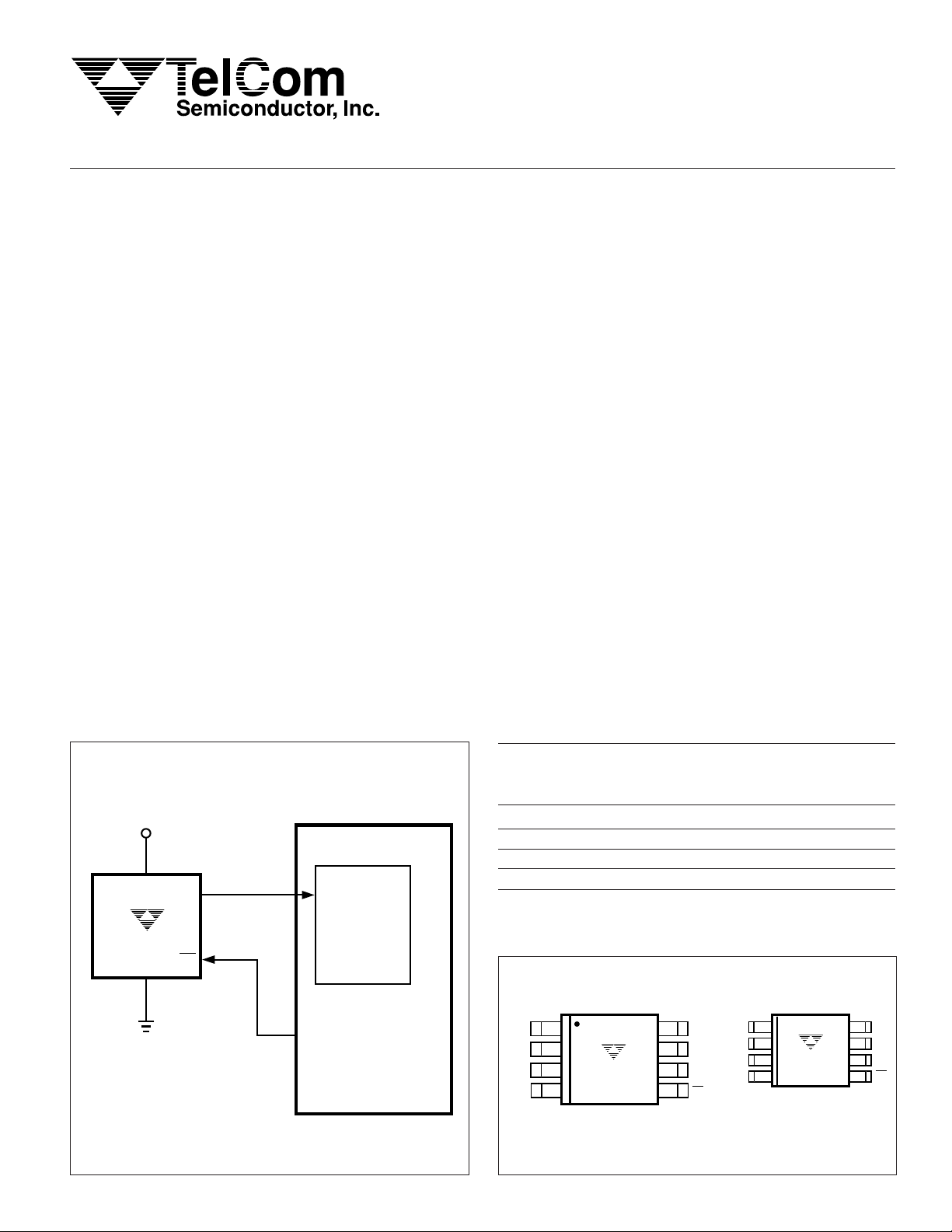
TYPICAL APPLICATION
GENERAL DESCRIPTION
The TC1023/1024 temperature sensors furnish a linearized output voltage directly proportional to measured
temperature. The TC1023 has a temperature measurement range of – 20°C to +100°C. Its output voltage is
directly calibrated in degrees Centigrade (i.e., V
OUT
=
10mV/°C x Temperature °C). An external pull-down resistor to a negative voltage source is required for temperature
measurement below 0°C.
The TC1024 has a temperature measurement range of
– 20°C to +125°C, and operates with a single supply. It has
the same output voltage slope with temperature as the
TC1023 (10mV/°C). The output voltage range is 100mV at
– 20°C to 1,750mV at +125°C. Both devices have a chip
enable input that reduces supply current to 1µA (typical)
when pulled active high. In this state, the output defaults to
a high resistance allowing an external reference voltage to
be directly connected for A/D calibration.
Small size, low cost, flexibility and low power operation
make the TC1023/1024 suitable for a wide range of general purpose temperature measurement applications.
ORDERING INFORMATION
V
= 2.2V to 12V
CC
VCC
TC1023
GND
TC1023/1024-05 6/12/97
Part No. Package At 25°C Temp. Range
TC1023VOA 8-Pin SOIC 250mV – 20°C to +100°C
MICROCONTROLLER
TC1023VUA 8-Pin MSOP 250mV – 20°C to +100°C
TC1024VOA 8-Pin SOIC 750mV – 20°C to +125°C
V
OUT
A/D
CONVERTER
TC1024VUA 8-Pin MSOP 750mV – 20°C to +125°C
PIN CONFIGURATION
CE
V
18
I/O LINE
TelCom Semiconductor reserves the right to make changes in the circuitry and specifications of its devices.
OUT
27
NC
NC
36
45
GND
1
8-Pin SOIC
TC1023VOA
TC1024VOA
Output
Voltage
V
CC
NC
NC
CE
V
OUT
NC
NC
GND
MSOP-8
1
2
TC1023VUA
3
TC1024VUA
4
8
V
CC
7
NC
6
NC
CE
5
Page 2
PRELIMINARY INFORMATION
TC1023
TC1024
PRECISION TEMPERATURE-TO-VOLTAGE
CONVERTERS WITH SHUTDOWN MODE
ABSOLUTE MAXIMUM RATINGS *
Supply Voltage ............................................................15V
Input Voltage, Any Terminal..............– 1.0 to (VCC +0.3V)
Operating Temperature (TC1023).........– 20°C to +100°C
Operating Temperature (TC1024).........– 20°C to +125°C
Storage Temperature ............................– 55°C to +150°C
Lead Temperature (Soldering, 10 sec) ................. +300°C
ELECTRICAL CHARACTERISTICS :
TA = – 20°C to +125°C, VCC = 5V ±5%,
* Static-sensitive device. Unused devices must be stored in conductive
material. Protect devices from static discharge and static fields. Stresses
above those listed under Absolute Maximum Ratings may cause permanent damage to the device. These are stress ratings only and functional
operation of the device at these or any other conditions above those
indicated in the operational sections of the specifications is not implied.
Exposure to Absolute Maximum Rating Conditions for extended periods
may affect device reliability.
GND = 0V, unless otherwise specified.
Symbol Parameter Test Conditions Min Typ Max Unit
V
CC
Supply Voltage (TC1023) 2.2 — 12 V
(TC1024) 3.0 — 12
I
S
Supply Current CE = V
IL
—4060 µA
(Note 1)
I
CE
Shutdown Current CE = V
IH
—1 5 µA
(Note 2)
V
V
I
CE
t
REC
IH
IL
CE Input Logic HIGH Level 2.0 — — V
CE Input Logic LOW Level — — 0.8 V
CE Input Leakage Current CE = V
Recovery Time from Shutdown CE = step from VIH to V
IH
or V
IL
IL
–1 — +1 µA
— 400 — µsec
(Note 3)
V
OUT
V
Output Voltage (TC1024) TA = – 20°C and +125°C 270 — 1780 mV
OUT
V
Output Voltage (TC1023) TA = – 20°C and +100°C – 230 — 1030
OUT
Circuit per Figure 1:
R1 = 240kΩ
V
= – 12V
SS
(Note 1)
I
SRC
V
Output Source Current — — 1.0 mA
OUT
Accuracy at Room Temperature
TA = +25°C – 2 — +2 °C
(Note 4)
Accuracy at Minimum Temperature TC1023: TA = – 20°C – 4 — +4 °C
TC1024: T
= – 20°C
A
(Note 4)
Accuracy at Maximum Temperature TC1023: TA = +100°C – 3 — +3 °C
TC1024: T
= +125°C
A
(Note 4)
Nonlinearity Note 5 – 0.8 — +0.8 °C
Line Regulation — 80 — µV/V
A
V
V
OUTMAX
Average Slope of Output Voltage — 10 — mV/°C
Maximum Output Voltage
TC1023: 2.2V ≤ VCC ≤ 12V
——V
– 1.2 V
CC
TC1024: 3.0V ≤ VCC ≤ 12V
(Note 1)
NOTES: 1. V
temperature driving a 100pF capacitive load.
outputs open circuited.
OUT
2. V
is 0V through approximately 100kΩ to ground when CE = VIH.
OUT
3. Recovery time is the period required for V
4. Accuracy = Difference between calculated output voltage (10mV/°C x Device case temperature at specified temperature and power
supply) and measured output voltage expressed in °C.
5. Nonlinearity = deviation of output voltage versus temperature from the best-fit straight line over the device rated temperature range.
to rise from 0V (shutdown state) to the voltage corresponding to the measured
OUT
TC1023/1024-05 6/12/97
2
Page 3

PRECISION TEMPERATURE-TO-VOLTAGE
TC102x
GND
CE
V
CC
V
CC
V
OUT
TC102x
GND
Zone 1/Zone 2
Zone 1
Zone 2
CE
V
CC
V
OUT
I/O Pin
MICROCONTROLLER
A/D
CONVERTER
CONVERTERS WITH SHUTDOWN MODE
PRELIMINARY INFORMATION
TC1023
TC1024
DETAILED DESCRIPTION
A plot of output voltage versus temperature for both the
TC1023 and TC1024 appears in Figure 5. The TC1023 can
be used with single power supply to measure temperatures
from 0°C to 100°C. A pull-down resistor (R1 in Figure 1)
must be added from the output pin to the negative power
supply for measuring temperatures less than 0°C. The
value of the resistor must be chosen to limit the maximum
current pulled from the output to the negative supply to
– 50µA (i.e., R1 = VSS/50µA).
Output Stage
Both devices have Class A output stages capable of
sourcing 1mA. These devices have a limited ability to drive
heavy capacitive loads. Loads of 50pF (to ground) can be
driven directly. For heavier loads, a 2kΩ (or greater) resistor should be placed in series with the output for decoupling.
If the TC1023/1024 is used in a noisy electrical environment, a 0.1µF bypass capacitor from VCC to GND is recommended.
Shutdown/Calibrate Mode
The TC1023/1024 enters shutdown when the CE input
is taken to VIH. This causes quiescent current to fall to 1µA
(typ) and the output to drop immediately to 0V through
approximately 100kΩ. For applications where the TC1023/
1024 is connected to an external A/D converter, a reference voltage can be directly connected to V
shutdown for A/D calibration, as shown in Figure 3. A
CMOS gate provides bias voltage to the bandgap reference VR, and at the same time disables the TC102x by
taking CE to VIH. Limiting resistor R1 should be chosen to
limit current through the voltage reference to the desired
current (I
). That is, R1 = (VOH – V
REF
REF
)/I
REF
is the CMOS gate output high voltage at output current
equal to I
; and V
REF
= 2.2V to 12.0V MIN.
V
CC
is the reference voltage of VR).
REF
while in
OUT
(where V
OH
= 3.0V to 12.0V
V
CC
V
CC
TC1024
CE
GND
TC1024 (– 20°C to +125°C)
Figure 2. TC1024 Connections
2.5V
REF
CE
V
CC
V
CC
V
TC102x
OUT
GND
Figure 3. A/D Calibration
V
OUT
CONVERTER
R1
A/D
V
OUT
CMOS
GATE
CAL
Multi-Zone Temperature Sensing
The CE input facilitates multi-zone temperature sensing as shown in the example of Figure 4. In this example,
the processor addresses either of two sensors with a single
I/O port pin. The TC102x V
and routed to the processor's A/D converter, eliminating
the need for separate A/D input channels for each sensor.
pins are connected together
OUT
TC1023/1024-05 6/12/97
V
CC
/50µA
V
OUT
Figure 4. TC1023/1024 Addressing
3
V
OUT
TC1023
CE
GND
Figure 1. TC1023 Connections
R1
= V
V
SS
SS
Page 4

PRELIMINARY INFORMATION
TC1023
TC1024
1.8
1.7
1.6
1.5
1.4
1.3
1.2
1.1
1.0
0.9
(VOLTS)
0.8
0.7
OUT
V
0.6
0.5
0.4
0.3
0.2
0.1
0
– 0.1
– 0.2
– 40
TC1023: V
TC1024: V
– 30 – 20
= (10mV/°C) (Temperature °C)
OUT
= (10mV/°C) (Temperature °C) + 500mV
OUT
TC1024
–10
0
PRECISION TEMPERATURE-TO-VOLTAGE
CONVERTERS WITH SHUTDOWN MODE
TC1023
10
30
20
50
40
60 70 80 90 100 110 120
130
TEMPERATURE (°C)
Figure 5. Output Voltage vs. Temperature
TC1023/1024-05 6/12/97
4
Page 5

PRECISION TEMPERATURE-TO-VOLTAGE
CONVERTERS WITH SHUTDOWN MODE
PACKAGE DIMENSIONS
8-Pin SOIC
PIN 1
PRELIMINARY INFORMATION
TC1023
TC1024
.050 (1.27) TYP.
.197 (5.00)
.189 (4.80)
.018 (0.46)
.014 (0.36)
.157 (3.99)
.150 (3.81)
.010 (0.25)
.004 (0.10)
.069 (1.75)
.053 (1.35)
PIN 1
.244 (6.20)
.228 (5.79)
8°MAX.
8-Pin MSOP
.010 (0.25)
.007 (0.18)
.050 (1.27)
.016 (0.40)
TC1023/1024-05 6/12/97
.026 (0.65) TYP.
.122 (3.10)
.114 (2.90)
.016 (0.40)
.010 (0.25)
.006 (0.15)
.002 (0.05)
.122 (3.10)
.114 (2.90)
.197 (5.00)
.187 (4.80)
.043 (1.10)
MAX.
6°MAX.
5
.008 (0.20)
.005 (0.13)
.028 (0.70)
.016 (0.40)
Dimensions: inches (mm)
Page 6

PRELIMINARY INFORMATION
TC1023
TC1024
PRECISION TEMPERATURE-TO-VOLTAGE
CONVERTERS WITH SHUTDOWN MODE
Sales Offices
TelCom Semiconductor
1300 Terra Bella Avenue
P.O. Box 7267
Mountain View, CA 94039-7267
TEL: 415-968-9241
FAX: 415-967-1590
E-Mail: liter@c2smtp.telcom-semi.com
TC1023/1024-05 6/12/97
TelCom Semiconductor
Austin Product Center
9101 Burnet Rd. Suite 214
Austin, TX 78758
TEL: 512-873-7100
FAX: 512-873-8236
6
TelCom Semiconductor H.K. Ltd.
10 Sam Chuk Street, Ground Floor
San Po Kong, Kowloon
Hong Kong
TEL: 852-2324-0122
FAX: 852-2354-9957
Printed in the U.S.A.
 Loading...