

Page 1
.tec
TBS6416B4E
M
1M x 16Bit x 4 Banks synchronous DRAM
GENERAL DESCRIPTION
The TBS6416B4E is 67,108,864 bits synchronous high data rate Dynamic RAM organized as 4 x 1,048,576 words by 16 bits,
fabricated with M’tec high performance CMOS technology. Synchronous design allows precise cycle control with the use of
system clock I/O transactions are possible on every clock cycle. Range of operating frequencies, programmable burst length and
programmable latencies allow the same device to be useful for a variety of high bandwidth, high performance memory system
applications.
FEATURES
•
JEDEC standard 3.3V power supply
• LVTTL compatible with multiplexed address
• Four-banks operation
• MRS cycle with address key programs
-. CAS latency (2 & 3)
-. Burst length (1, 2, 4, 8 & Full page)
-. Burst type (Sequential & Interleave)
•
All inputs are sampled at the positive going edge of the system clock.
• Burst read single-bit write operation
• DQM for masking
• Auto & self refresh
• 64ms refresh period (4K cycle)
ORDERING INFORMATION
Part No.
TBS6416B4E-7G 143MHz LVTTL
Max Freq.
Interface Package
54
TSOP(II)
Revision_1.1
1
Sep. 2000
Page 2
M
.tec
TBS6416B4E
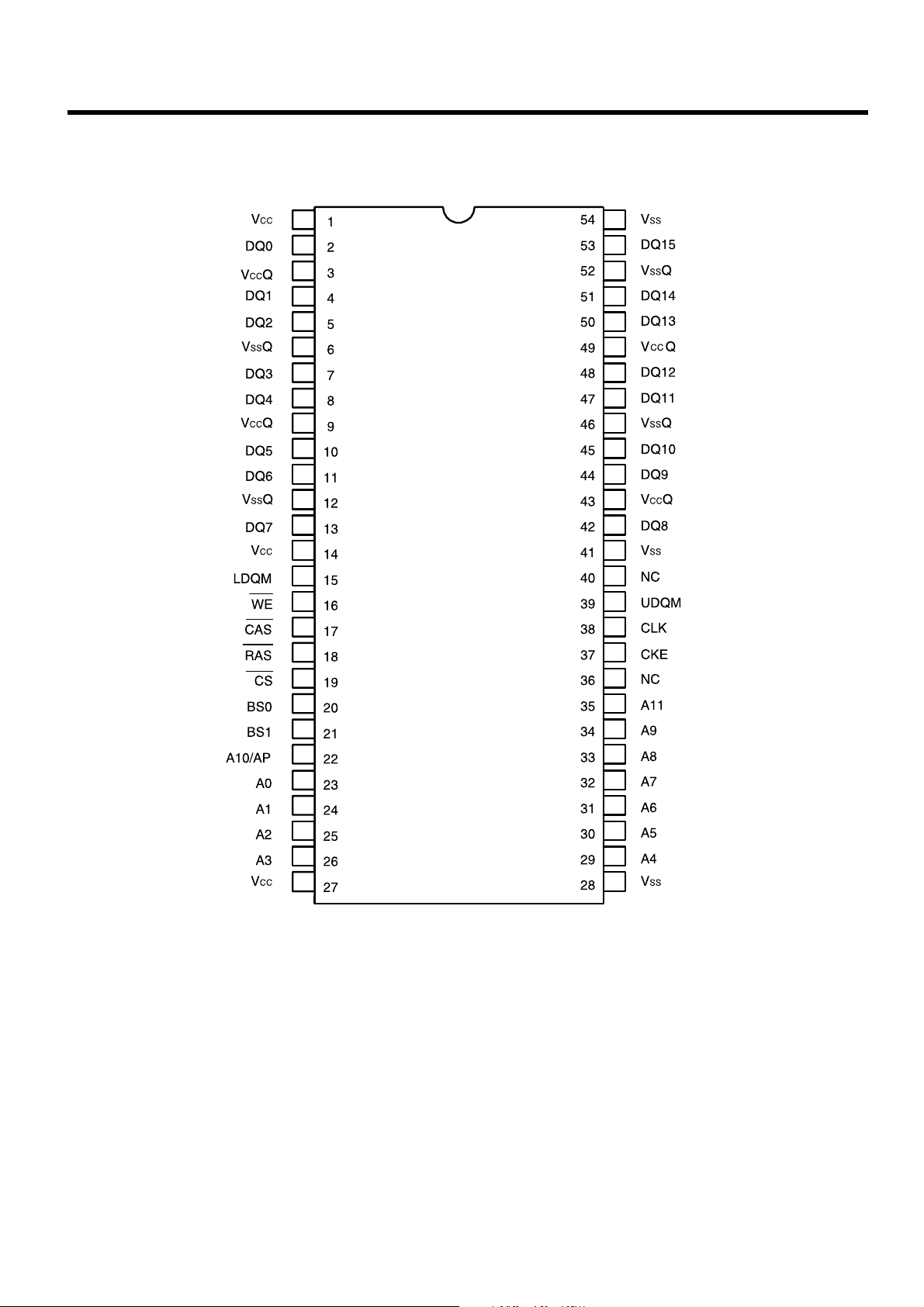
PIN CONFIGURATION
(Top View)
2
Revision_1.1
Sep. 2000
54Pin TSOP (II)
(400mil x 875mil)
(0.8 mm Pin pitch)
Page 3
.tec
TBS6416B4E
M
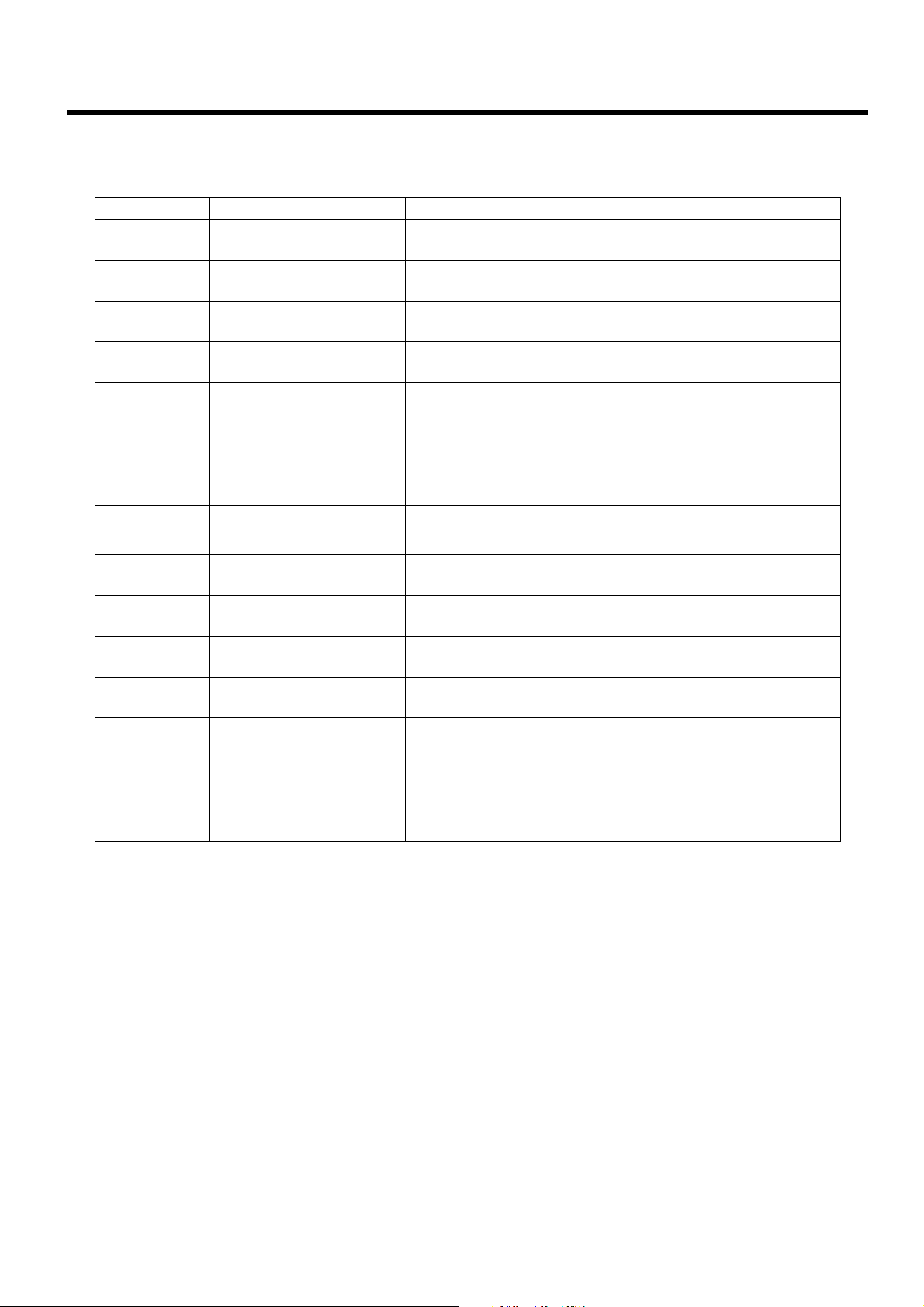
PIN FUNCTION DESCRIPTION
Pin Name
A0~ A11
BS0, BS1
DQ0 ~DQ15
/CS Chip Select Disable or enable the command decoder. When command decod er i s
/RAS Row Address Strobe
/CAS Column Address Strobe
/WE Write Enable Referred to /RAS
Address
Bank
Data Input / Output Multiplexed pins for data output and input.
Function
Multiplexed pins for row and column address Row address: A0~ A11.
Column address: A0 ~ A7.
Select bank to activate during row address latch time, or bank to
read/write during address latch time.
disabled, new command is ignored and previous operation continues.
Command input. When sampled at the rising edge of the clock, /RAS,
/CAS and /WE define the operation to be executed.
Referred to /RAS
Description
UDQM/LDQM Input /output mask
CLK Clock Input System clock used to sample inputs on the rising edge of clock.
CKE Clock Enable CKE controls the clock activation and deactivation. When CKE is low,
Vcc Power (+3.3 V) Power for input buffers and logic circuit inside DRAM.
Vss Ground Ground for input buffers and logic circuit inside DRAM.
Vcc Q Power (+ 3.3 V) for I/O
buffer
Vss Q Ground for I/O buffer Separated ground from
NC No Connection No connection
The output buffer is placed at Hi-Z (with latency of 2) when DQM is
sampled high in read cycle. In write cycle, sampling DQM high will
block the write operation with zero latency.
Power Down mode, Suspend mode, or Self Refresh mode is entered.
Separated power from
VCC
, used for output buffers to improve noise.
VSS
, used for output buffers to improve noise.
Revision_1.1
3
Sep. 2000
Page 4
.tec
TBS6416B4E
M
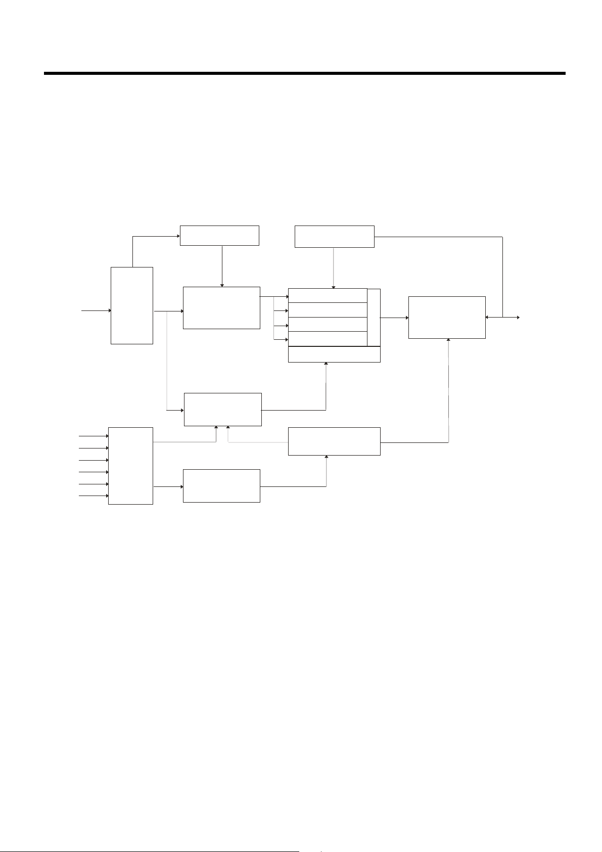
FUNCTIONAL BLOCK DIAGRAM
ADD
/CS
/ RAS
/ CAS
/ WE
CLK
CKE
Address
Buffer
Commend
Decoder
&
Clock
Buffer
Bank Select
Row Decoder
&
Refresh Counter
Column Buffer
Programming
Register
Data Input
1Mx16
1Mx16
1Mx16
1Mx16
Column Decoder
Latency &
Burst Length
Sense AMP
Output Buffer
DQ
Revision_1.1
4
Sep. 2000
Page 5
.tec
TBS6416B4E
M
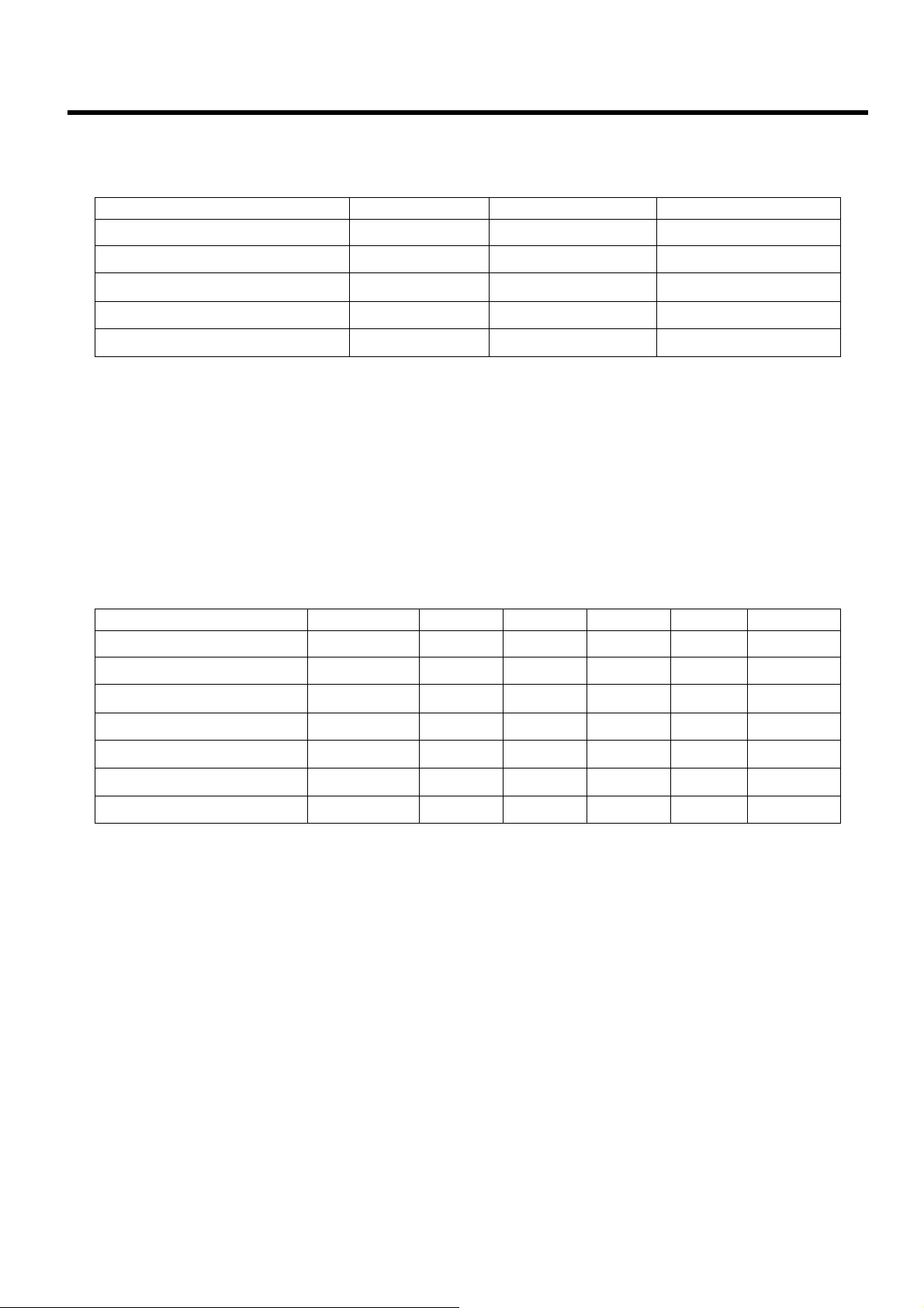
ABSOLUTE MAXIMUM RATING
Parameter Symbol
SS
Voltage on any pin relative to V
VIN, V
OUT
Value
-1.0 ~ 4.6
Unit
V
T
STG
P
OS
I
Q
D
-1.0 ~ 4.6
-55 ~ +150
50
1
Voltage on VCC supply relative to VSS
Storage temperature
Power dissipation
Short circuit current
VCC, VCC
Note:
Permanent device damage may occur if "ABSOLUTE MAXIMUM RATINGS" are exceeded.
Functional operation should be restricted to the recommended operating conditions.
Exposure to higher voltage than recommended for extended periods of time could affect device reliability.
DC OPERATING CONDITIONS
Recommended operating conditions (Voltage referenced to VSS = 0V, TA = 0 to 70°C)
Parameter Symbol Min
Supply voltage
Input logic high voltage
Input logic low voltage
VCC, VCC
Q
IH
V
IL
V
3.0
2.0
-0.3
Typ Max Unit
3.3 3.6 V
3.0 VCCQ+0.3 V
0 0.8 V 2
V
℃
W
mA
Note
1
OH
V
OL
V
IL
IL
Q
2.4
-
-1 - 1 uA 3
-1.5 - 1.5 uA 3,4
- - V IOH=-2mA
- 0.4 V IOL=2mA
≦
VCC
out
Q,
≦
VCC
Output logic high voltage
Output logic low voltage
Input leakage current (Input) I
Input leakage current (I/O pins) I
Notes:
1.
2. V
3. Any input 0V ≦ V
Input leakage currents include Hi-Z output leakage for all bi-directional buffers with Tri-State outputs.
4. D
IH
V
(max) = 5.6V AC. The overshoot voltage duration is ≦ 3ns.
IL
(min) = -2.0V AC. The undershoot voltage duration is ≦ 3ns.
IN
out
is disabled, 0V ≦ V
Revision_1.1
5
Sep. 2000
Page 6
.tec
TBS6416B4E
M
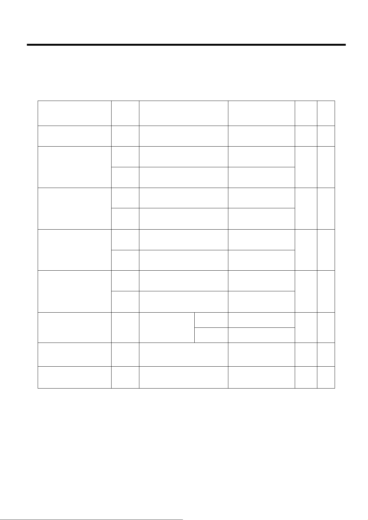
DC CHARACTERISTICS
(Recommended operating condition unless otherwise noted, TA = 0 to 70°C)
Parameter Symbol Test Condition TBS6416B4E-7G
Operating current
(One bank active)
Pre-charge standby current
in power- down mode
Pre-charge standby current
in non power-down mode
Active standby current in
power-down mode
Active standby current in
non power-down mode
(One bank active)
Operating current
(Burst mode)
I
CC2
I
CC3
I
I
CC3
I
CC1
I
CC2
I
CC2
CC2
I
CC3
I
CC3
CC4
I
Burst length = 1
RC
RC
≧
t
t
(min)
IOL = 0mA
CKE≦V
P
CKE&CLK≦V
PS
CKE≧V
N
CC
t
IL
IH
= 15ns
(max), t
CC
= 15 ns
IL
(max), t
(min), /CS≧VIH(min) ,
Input signals are stable
CKE≧VIH(min), CLK≦VIL(Max) ,
CC
NS
t
∞
=
Input signals are stable
CKE≦V
P
CKE&CLK≦V
PS
CKE≧V
N
CC
t
IL
IH
= 15ns
(max), t
CC
= 15 ns
IL
(max), t
(min), /CS≧VIH(min) ,
Input signals are stable
CKE≧VIH(min), CLK≦VIL(Max) ,
NS
t
CC
∞
=
Input signals are stable
IOL=0 mA
Page burst
2Banks activated
CCD
t
= 2CLK
S
100 mA 1
CC
∞
=
2
2
30
10
5
CC
∞
=
5
40
20
CL = 3 150
CL = 2 140
Unit Note
mA
mA
mA
mA
mA
1
RC
tRC(min)
t
Refresh current I
Self refresh current I
CC5
CC6
CKE≦0.2V
≧
Note:
1.Measured with outputs open.
2.Refresh period is 64 ms.
Revision_1.1
160
1 mA
6
Sep. 2000
mA
2
Page 7
.tec
TBS6416B4E
M
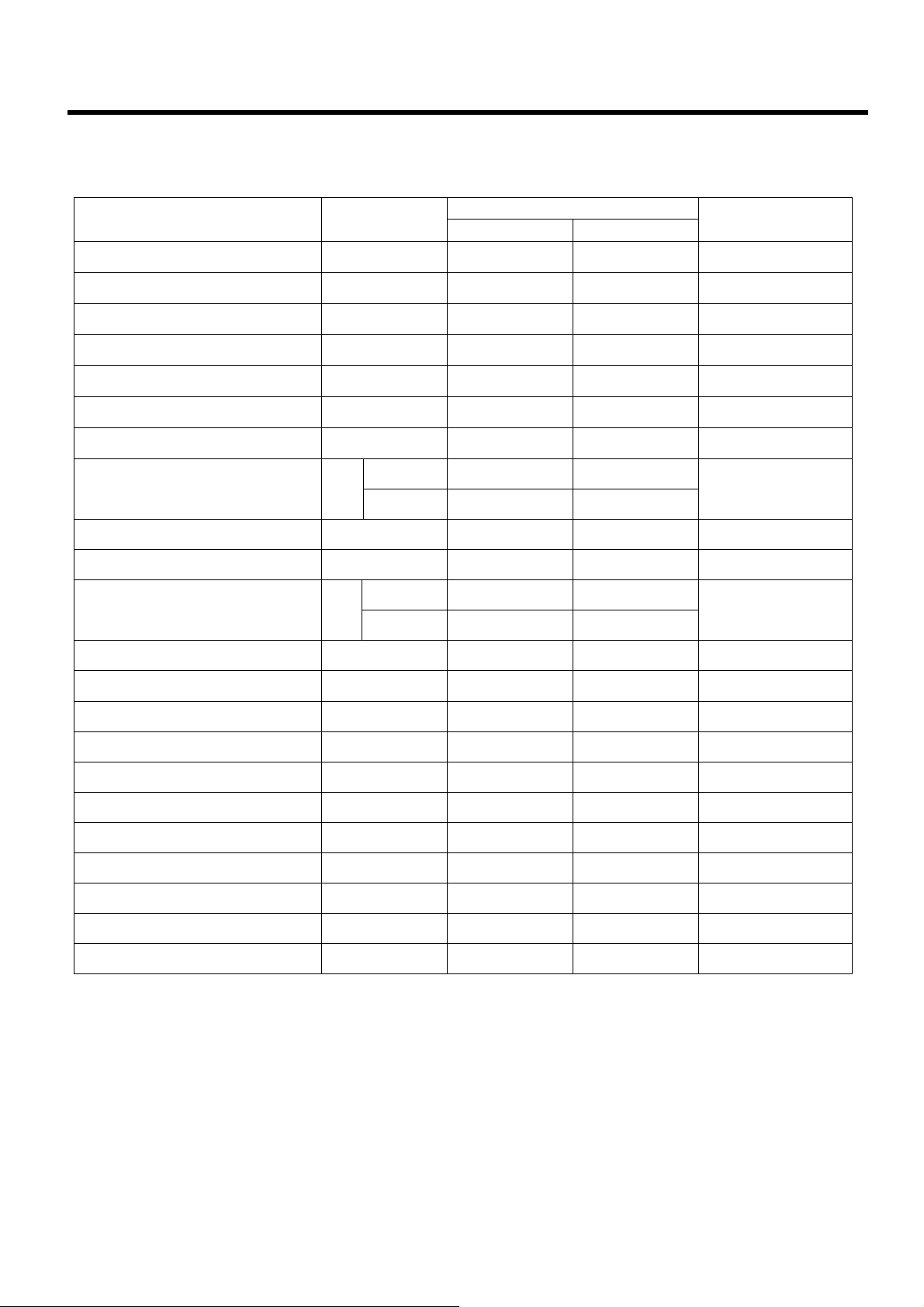
AC CHARACTERISTICS AND OPERATING CONDITION FOR PC-143
(Vcc=3.3V±0.3V, Ta=0° to 70°C)
Parameter Symbol
TBS6416B4E-7G
Min Max
Unit
Row active to row active delay t
/RAS to /CAS delay t
Row pre-charge time tRP 20 ns
Row active time t
Row cycle time tRC 63 ns
Col. Address to col. Address delay t
Write Recovery Time tWR 14 ns
CLK Cycle Time tCK
CLK High Level width tCH 2.5 ns
CLK Low Level width tCL 2.5 ns
Access Time from CLK tAC
Output Data Hold Time tOH 2.5 ns
Data-in Set-up Time tDS 1.5 ns
RRD
14 ns
RCD
20 ns
RAS
CCD
1 CLK
CL=2 10 1000
CL=3 7 1000
CL=2 6
CL=3 5.4
45 100K ns
ns
ns
Data-in Hold Time tDH 1 ns
Address Set-up Time tAS 1.5 ns
Address Hold Time tAH 1 ns
CKE Set-up Time t
CKE Hold Time t
Command Set-up Time t
Command Hold Time t
Refresh Time t
Mode register Set Cycle Time t
CKS
1.5 ns
CKH
1 ns
CMS
1.5 ns
CMH
1 ns
REF
64 ms
RSC
15 ns
Revision_1.1
7
Sep. 2000
Page 8
.tec
TBS6416B4E
M
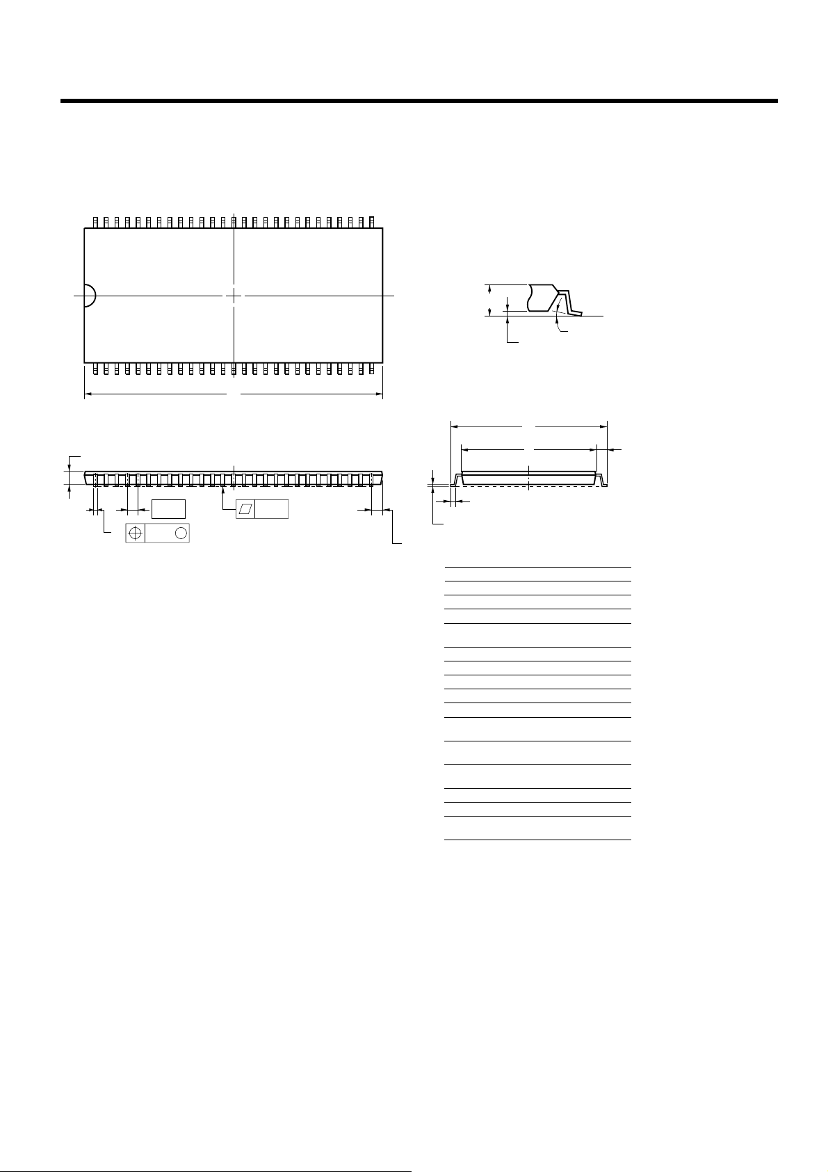
54PIN PLASTIC TSOP(II) (400mil)
54 28
detail of lead end
F
12 7
G
CN
D
NOTE
Each lead centerline is located within 0.13 mm (0.005 inch) of
its true position (T.P.) at maximum material condition.
M
M
A
K
B
E
H
I
L
ITEM MILLIMETERS INCHES
A 22.62 MAX. 0.891 MAX.
B 0.91 MAX. 0.036 MAX.
C 0.80 (T.P.) 0.031 (T.P.)
+7°
–3°
+0.08
–0.07
+0.025
–0.015
D 0.32 0.013±0.003
E 0.10±0.05 0.004±0.002
F 1.20 MAX. 0.048 MAX.
G 1.00 0.039
H 11.76±0.20 0.463±0.008
I 10.16±0.10 0.400±0.004
J 0.80±0.20 0.031
K 0.145 0.006±0.001
L 0.50±0.10 0.020
M 0.13 0.005
N 0.10 0.004
P3°
P
+0.009
–0.008
+0.004
–0.005
+7°
3°
–3°
J
Revision_1.1
8
Sep. 2000
 Loading...