

Page 1
TB62201AFG
TOSHIBA Bi-CMOS Processor IC Silicon Monolithic
TB62201AFG
Dual-Stepping Motor Driver IC for OA Equipment Using PWM Chopper Type
The TB62201AFG is a dual-stepping motor driver driven by
chopper micro-step pseudo sine wave.
To drive two-phase stepping motors, Two pairs of 16-bit latch and
shift registers are built in the IC. The IC is optimal for driving
stepping motors at high efficiency and with low-torque ripple.
The IC supports Mixed Decay mode for switching the attenuation
ratio at chopping. The switching time for the attenuation ratio
can be switched in four stages according to the load.
Features
z Two stepping motors driven by micro-step pseudo sine wave
are controlled by a single driver IC
z Monolithic Bi-CMOS IC
z Low ON-resistance of Ron = 0.5 Ω (T
z ESD protection Exceeds 2000 V, MIL-STD-883D
z Two pairs of built-in 16-bit shift and latch registers
z Two pairs of built-in 4-bit DA converters for micro steps
z Built-in ISD, TSD, V
z Built-in charge pump circuit (two external capacitors)
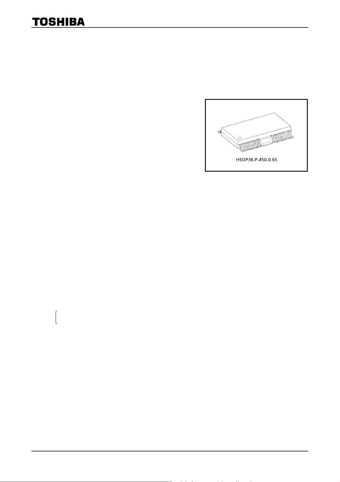
z 36-pin power flat package (HSOP36-P-450-0.65)
z Output voltage: 40 V max
z Output current: 1.5 A/phase max
z Built-in Mixed Decay mode enables specification of four-stage attenuation ratio.
(The attenuation ratio table can be overwritten externally.)
z Chopping frequency can be set by external resistors and capacitors. High-speed chopping possible at 100 kHz or
higher.
DD&VM
power monitor (reset) circuit for protection
= 25°C @ 1.0 A: typ.)
j
Weight: 0.79 g (typ.)
Note: When using the IC, pay attention to thermal conditions.
These devices are easy damage by high static voltage.
In regards to this, please handle with care.
1
2005-04-04
Page 2
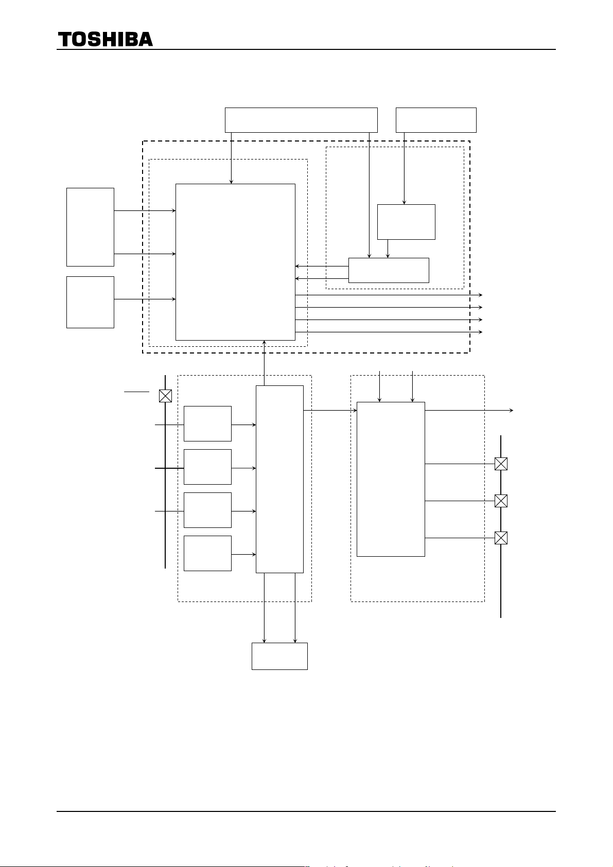
Block Diagram
1. Overview (Power lines: A/B unit (C/D unit is the same as A/B unit))
TB62201AFG
RESET
SETUP
DATA
CLK
STROBE
V
R
V
ref
Mixed decay timing, table logic circuit
DATA
input
selector
Current Setting
Torque
control
16-bit shift
register
Current control data logic circuit
16-bit shift
register
(angle control)
16-bit latch
4-bit D/A
16-bit latch
Mixed decay
timing table
selector
Chopping reference
circuit
Chopping
waveform
generator
circuit
Waveform
shaping
circuit
CR
Current feedback circuit
S
M
V
RS
circuit 1
V
RS
circuit 2
RS COMP
circuit 1
Output control circuit
RS COMP
circuit 2
cp2
C
cp1
C
Charge
pump
circuit
High-Voltage Wiring (VM)
Logic data
Analog data
IC Terminal
Output circuit
(H-bridge)
Stepping
motor
Out X
circuit
V
M
Protected circuit
ISD
V
DDR/VMR
circuit
TSD
circuit
V
DD
2
2005-04-04
Page 3
2. Logic Unit A/B (C/D unit is the same as A/B unit)
Function
This circuit is used to input from the DATA pins micro-step current setting data and to transfer them to the
subsequent stage. By switching the SETUP pin, the data in the mixed decay timing table can be
overwritten.
Mixed decay timing table logic circuit
TB62201AFG
SETUP
DATA
CLK
STROBE
Initial
setup
circuit
Data input
selector
Mixed
decay
timing
table 1
16-bit latch
0 1 2 3 4 5 6 7 8 9 10 11 12 13 14 15
0 1 2 3 4 5 6 7 8 9 10 11 12 13 14 15
16-bit shift register
Micro-step current setting data logic circuit
16-bit shift register
0 1 2 3 4 5 6 7 8 9 10 11 12 13 14 15
0 1 2 3 4 5 6 7 8 9 10 11 12 13 14 15
16-bit latch
Mixed
decay
timing
table 2
Mixed
decay
timing
table 3
Mixed
decay
timing
table 4
A unit side
Mixed
decay
timing
table selector
Mixed
decay
timing
Output
control
circuit
Torque
× 2 bits
RESET
Current feedback circuit D/A circuit
Decay
× 2 bits
B unit side
Current
× 4 bits
B unit side
Output control circuit
Note: The RESET and SETUP pins are pulled down in the IC by 10 kΩ resistor.
When not using these pins, connect them to GND. Otherwise, malfunction may occur.
Phase
× 1 bit
B unit side
3
2005-04-04
Page 4
TB62201AFG
ng
3. Current Feedback Circuit and Current Setting Circuit
(A/B unit (C/D unit is the same as A/B unit))
Function
The current setting circuit is used to set the reference voltage of the output current using the micro-step
current setting data input from the DATA pins.
The current feedback circuit is used to output to the output control circuit the relation between the set
current value and output current. This is done by comparing the reference voltage output to the current
setting circuit with the potential difference generated when current flows through the current sense
resistor connected between RS and V
The chopping waveform generator circuit to which CR is connected is used to generate clock used as
reference for the chopping frequency.
.
M
TORQUE
0, 1
V
ref
R
S
100%
85%
70%
50%
TORQUE
control
circuit
Current setting circuit
Logic
V
circuit 1
RS
(detects
potential
difference
between
RS and VM)
unit
CURRENT
15
14
13
12
11
10
9
8
7
6
5
4
3
2
1
0
0 to 3
Micro-step
current
setting
selector
circuit
4-bit
D/A
circuit
RS COMP
circuit 1
(Note 1)
m
or
circuit
generat
wavefor
Waveform shaping circuit
Chopping reference circuit
Output stop signal (ALL OFF)
Use in Charge mode
NF
(set current
reached signal)
CR
Mixed
decay
timing
circuit
Output
control
circuit
VM
Current feedback circuit
V
circuit 2
RS
(detects
potential
difference
between
VM and RS)
RS COMP
circuit 2
(Note 2)
RNF
(set current
monitor signal)
Use in Fast mode
Note 1: RS COMP 1: Compares the set current with the output current and outputs a signal when the output current
reaches the set current.
Note 2: RS COMP 2: Compares the set current with the output current at the end of Fast mode during chopping.
Outputs a signal when the set current is below the output current.
4
2005-04-04
Page 5
TB62201AFG
y
4. Output Control Circuit, Current Feedback Circuit and Current Setting Circuit
(A/B unit (C/D unit is the same as A/B unit))
Micro-step current setting
Output control circuit Phase
Current
feedback
circuit
Current
setting
circuit
RESET
Output pin
V
M
NF
set current
reached signal
RNF
set current
monitor signal
Output stop
signal
Output control circuit
ISD (current
charge start
shutdown)
circuit
VMR
circuit
data logic circuit
Mixed
decay
timing
Output reset signal
Reset signal
selector
circuit
Chopping
reference circuit
Decay
mode
counter
CR counter
U
1
U
2
L
1
L
2
V
DD
Charge
pump
halt
signal
Charge pump
circuit
CR
VM
Mixed
decay
timing
circuit
Power suppl
for upper
output MOS
transistors
V
H
Output
circuit
Output
circuit
Ccp A
V
V
DD
DDR
circuit
Thermal
shut down
(TSD)
circuit
Protection circuit
Micro-step
current
setup latch clear
signal
Logic
Note: The RESET pins is pulled down in the IC by 10-kΩ resistor.
When not using the pin, connect it to GND. Otherwise, malfunction may occur.
Mixed decay
timing table
clear signal
Charge pump
circuit
V
: VDD power on Reset
DDR
VMR: VM power on Reset
ISD: Current shutdown circuit
TSD: Thermal shutdown circuit
Ccp B
Ccp C
5
2005-04-04
Page 6
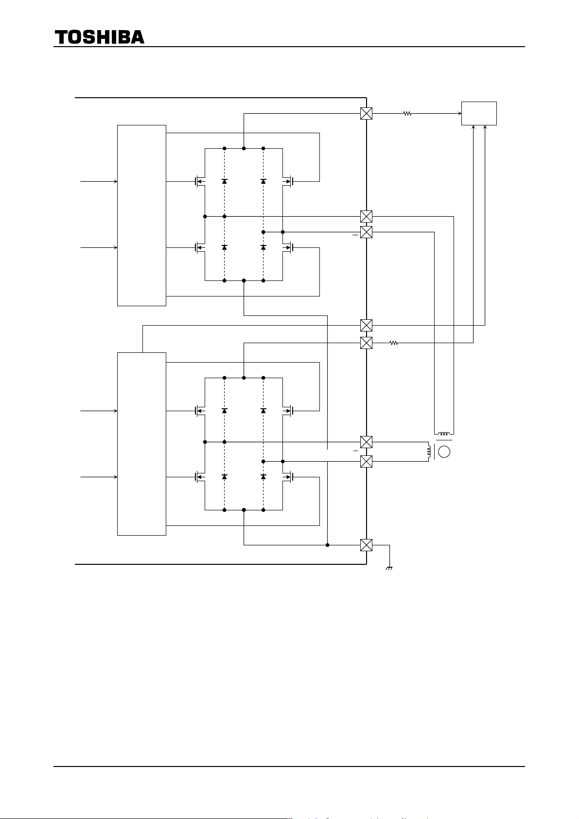
5. Output Equivalent Circuit (A/B unit (C/D unit is the same as A/B unit))
R
From
output
control
circuit
Output driver
circuit
U
1
U
2
L
1
L2
Power supply
for upper
output MOS
transistors
(VH)
Phase A
U1
L
S A
U
2
Output A
1
L2
Output
A
R
RS A
V
M B
TB62201AFG
To V
M
R
From
output
control
circuit
Output driver
circuit
U
1
U
2
L
1
L2
Power supply
for upper
output MOS
transistors
(VH)
Phase B
U1
L
S B
U
2
Output B
Output B
1
L2
R
RS B
PGND
M
6
2005-04-04
Page 7
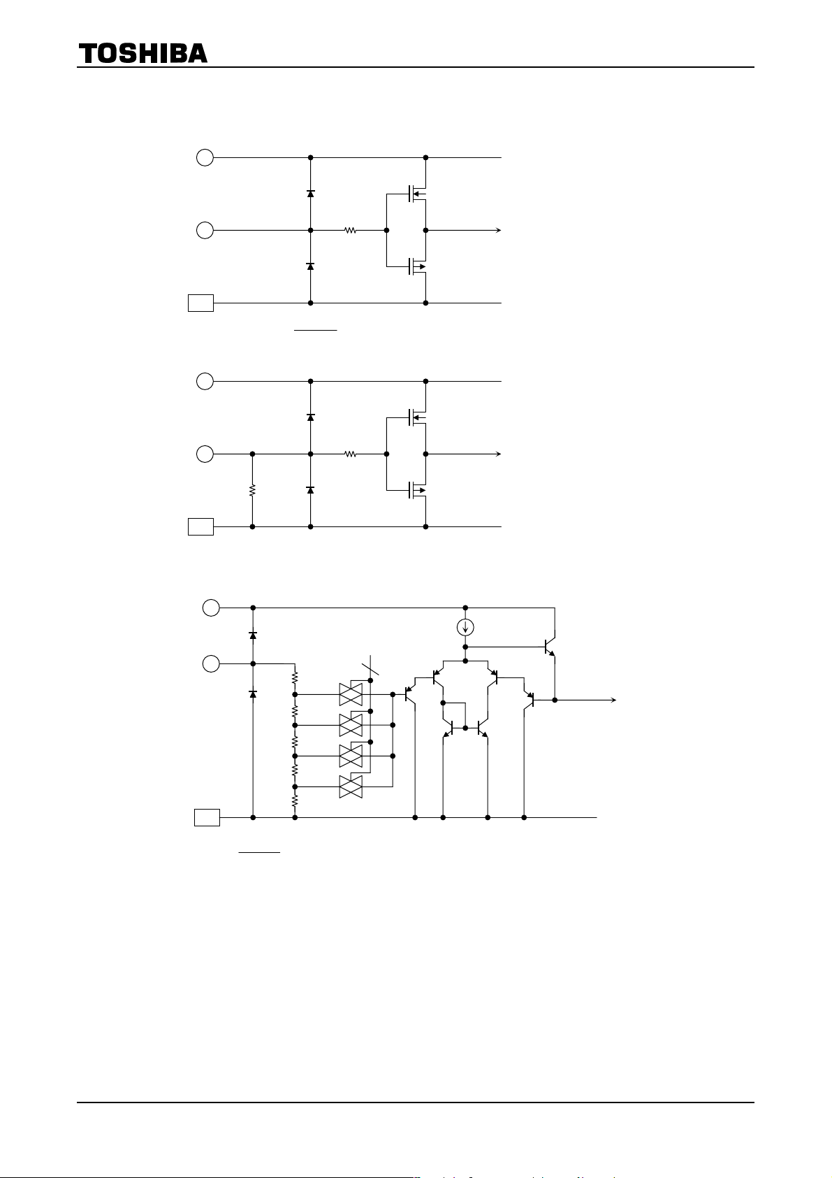
6. Input Equivalent Circuit
(1) Logic input circuit (CLK, DATA, STROBE)
VDD
27
IN
30/29/31
25/26/24
GND
FIN
(2) Input circuit (SETUP,
VDD
27
IN
6/28
RESET
TB62201AFG
To logic IC
150 Ω
)
To logic IC
150 Ω
GND
FIN
10 kΩ
(3) V
input circuit
ref
VDD
27
IN
9/10
GND
FIN
4
Note: The SETUP and RESET pins are pulled down. Do not use them open.
When not using these pins, connect them to GND.
To D/A circuit
7
2005-04-04
Page 8
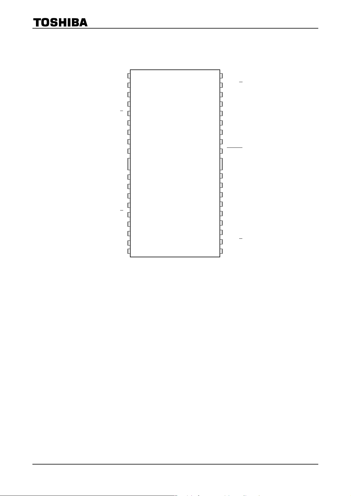
Pin Assignment
TB62201AFG
(Top view)
OUT B
OUT
SETUP
V
REF AB
V
SS
V
REF CD
OUT
OUT D
V
M B
R
S B
PGND
B
Ccp A
CR
(FIN)
NC
Ccp B
Ccp C
D
PGND
R
S D
V
MD
1
2
3
4
5
6
7
8
9
TB62201AFG
10
11
12
13
14
15
16
17
18
36
35
34
33
32
31
30
29
28
27
26
25
24
23
22
21
20
19
V
M A
OUT
A
R
S A
PGND
OUT A
STROBE AB
CLK AB
DATA AB
RESET
V
(FIN)
SS
V
DD
DATA CD
CLK CD
STROBE CD
OUT C
PGND
R
S C
C
OUT
V
MC
Note: [Important] If this IC is inserted reverse, voltages exceeding the voltages of standard may be applied to some
pins, causing damage.
Please confirm the pin assignment before mounting and using the IC.
8
2005-04-04
Page 9

Pin Description
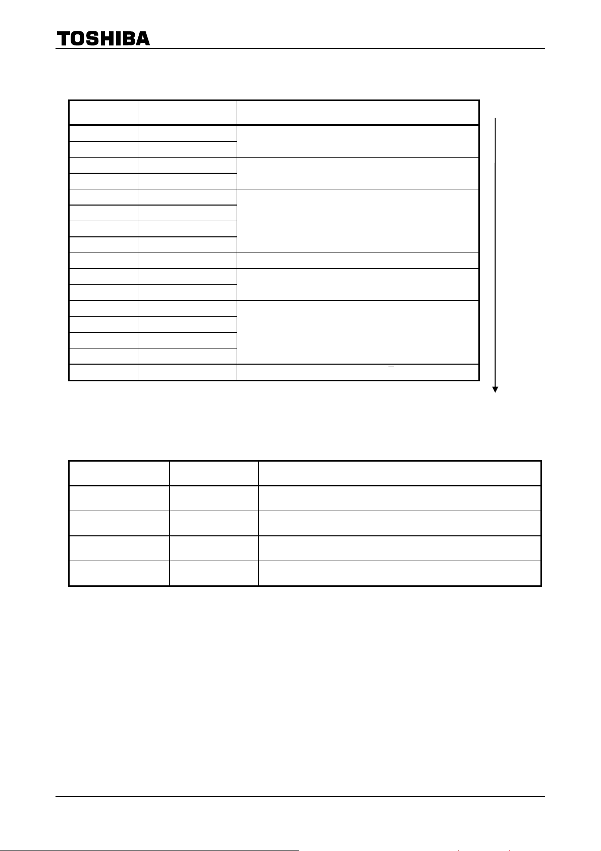
Pin No. Pin Symbol Description
TB62201AFG
1 V
2 OUT B Output B pin
3 R
4 PGND Power GND pin
5 B OUT Output B pin
6 SETUP CR setup switching pin (L: normal, H: setup)
7 Ccp A Capacitor pin for charge pump (Ccp1)
8 CR External C/R (osc) pin (sets chopping frequency)
9 V
FIN V
10 V
11 NC Non conection
12 Ccp B Capacitor pin for charge pump (Ccp2)
13 Ccp C Capacitor pin for charge pump (Ccp2)
14 D OUT Output D pin
15 PGND Power GND pin
16 R
17 OUT D Output D pin
18 V
19 V
20 C OUT Output C pin
21 R
22 PGND Power GND pin
23 OUT C Output C pin
24 STROBE CD CD STROBE (latch) signal input pin ( : LATCH)
25 CLK CD CD clock input pin
26 DATA CD CD serial data signal input pin
27 VDD Power pin for logic block
FIN V
28 RESET Output reset signal input pin (L: RESET)
29 DATA AB AB serial data signal input pin
30 CLK AB AB clock input pin
31 STROBE AB AB STROBE (latch) signal input pin ( : LATCH)
32 OUT A Output A pin
33 PGND Power GND pin
34 R
35 A OUT Output A pin
36 V
Voltage major for output B block
M B
Channel B current pin
S B
V
REF AB
FIN (VSS): Logic GND pin
SS
Vref input pin CD
REF CD
Channel D current pin
S D
Voltage major for output D block
M D
Voltage major for output C block
M C
Channel C current pin
S C
FIN (VSS) : Logic GND pin
SS
Channel A current pin
S A
Voltage major for output A block
M A
input pin AB
ref
Note: How to handle GND pins
All power GND pins and FIN (V
Since FIN also functions as a heat sink, take the heat dissipation into consideration when designing the board.
: signal GND) pins must be grounded.
SS
9
2005-04-04
Page 10
Signal Functions
TB62201AFG
1. Serial Input Signals
Data No. Name Functions
0 LSB TORQUE 0
1 TORQUE 1
2 DECAY MODE B0
3 DECAY MODE B1
4 Current B0
5 Current B1
6 Current B2
7 Current B3
8 PHASE B Phase information (H: OUT A: H, OUT A: L)
9 DECAY MODE A0
10 DECAY MODE A1
11 Current A0
12 Current A1
13 Current A2
14 Current A3
15 MSB PHASE A Phase information (H: OUT A: H, OUT A: L)
(for A/B. C/D is the same as A/B)
DATA No.0, 1
HL: 70%, LL: 50%
00: DECAY MODE 0, 01: DECAY MODE 1
10: DECAY MODE 2, 11: DECAY MODE 3
Used for setting current.
(LLLL
4-bit current B data
(Steps can be divided into 16 by 4-bit data)
00: DECAY MODE 0, 01: DECAY MODE 1
10: DECAY MODE 2, 11: DECAY MODE 3
Used for setting current.
(LLLL
4-bit current A data
(Steps can be divided into 16 by 4-bit data)
= HH: 100%, LH: 85%
= Output ALL OFF MODE)
= Output ALL OFF MODE)
(Note 1)
Note 1: Serial data input order
Serial data are input in the order LSB (DATA 0)
→ MSB (DATA 15)
Role of Data
Data Name Number of Bits Functions
TORQUE 2
DECAY MODE 2 × 2 phases
CURRENT 4 × 2 phases
PHASE 1 × 2 phases
Roughly regulates the current (four stages).
Common to A and B units.
Selects Decay mode.
A and B units are set separately.
Sets a 4−bit micro−step electrical angle.
A and B units are set separately.
Determines polarity (
A and B units are set separately.
+ or −).
10
2005-04-04
Page 11
2. Serial Input Signal Functions
Input Action
CLK STROBE DATA RESET
× × H H L
× H H H L
× L H H L
× × H H L
× × H H L
× × × L × L
× × × × L L
× × × H H H
×: Don’t Care
Qn: Latched output level when STROBE is .
Note 1: V
DDR
and VMR
H when the operable range (3 V typical) or higher and L when lower.
When one of V
or VMR is operating, the system resets (OR relationship).
DDR
Note 2: High when TSD is in operation.
When one of TSD or ISD is operating, the system resets (OR relationship).
Note: Function of overcurrent protection circuit
Until the RESET signal is input after ISD is triggered, the overcurrent protection circuit remains in operation.
During ISD, the charge pump stays halted.
When TSD and ISD are operating, the charge pump halts.
3. PHASE Functions
VDDR
(Note 2) or
V
MR
Operation of
TSD/ISD
TB62201AFG
(Note 2)
No change in shift register.
H level is input to shift register.
L level is input to shift register.
Shift register data are latched.
Qn
Output off, charge pump halted
(S/R DATA CLR)
Output off (S/R DATA CLR)
Charge pump halted
Mixed decay timing table cleared (only V
Output off (S/R DATA HOLD)
Charge pump halted
Restored when
RESET goes from Low to High
DDR
)
Input Function
H Positive polarity (A: H, Α : L)
L Negative polarity (A: L, Α : H)
11
2005-04-04
Page 12
4. DECAY Mode X0, X1 Functions
DECAY MODE X1 DECAY MODE X0 Function
TB62201AFG
L L
L H
H L
H H
Decay mode 0
(Initial value: SLOW DECAY MODE)
Decay mode 1
(Initial value: MIXED DECAY MODE: 37.5%)
Decay mode 2
(Initial value: MIXED DECAY MODE: 75%)
Decay mode 3
(Initial value: FAST DECAY MODE)
5. TORQUE Functions
TORQUE 0 TORQUE 1 Comparator Reference Voltage Ratio
H H 100%
L H 85%
H L 70%
L L 50%
6. Current AX (BX) Functions
Step
16 90.0 H H H H L L L L
15 84.4 H H H H L L L H
14 78.8 H H H L L L H L
13 73.1 H H L H L L H H
12 67.5 H H L L L H L L
11 61.2 H L H H L H L H
10 56.3 H L H L L H H L
9 50.6 H L L H L H H H
8 45.0 H L L L H L L L
7 39.4 L H H H H L L H
6 33.8 L H H L H L H L
5 28.1 L H L H H L H H
4 22.5 L H L L H H L L
3 16.9 L L H H H H L H
2 11.3 L L H L H H H L
1 5.6 L L L H H H H H
0 0.0 L L L L H H H H
Set Angle
A3 A
A
2
A
1
By inputting the above current data (A: 4-bit, B: 4-bit), 17-microstep drive is possible. For 1 step fixed to 90
degrees, see the section on output current vector line (83 page).
B
0
B
3
B
2
B
1
0
12
2005-04-04
Page 13
TB62201AFG
7. SETUP Functions
Input Function
H Decay timing data input mode
L Normal operating mode
Note: The SETUP pin is pulled down in the IC by 10-kΩ resistor.
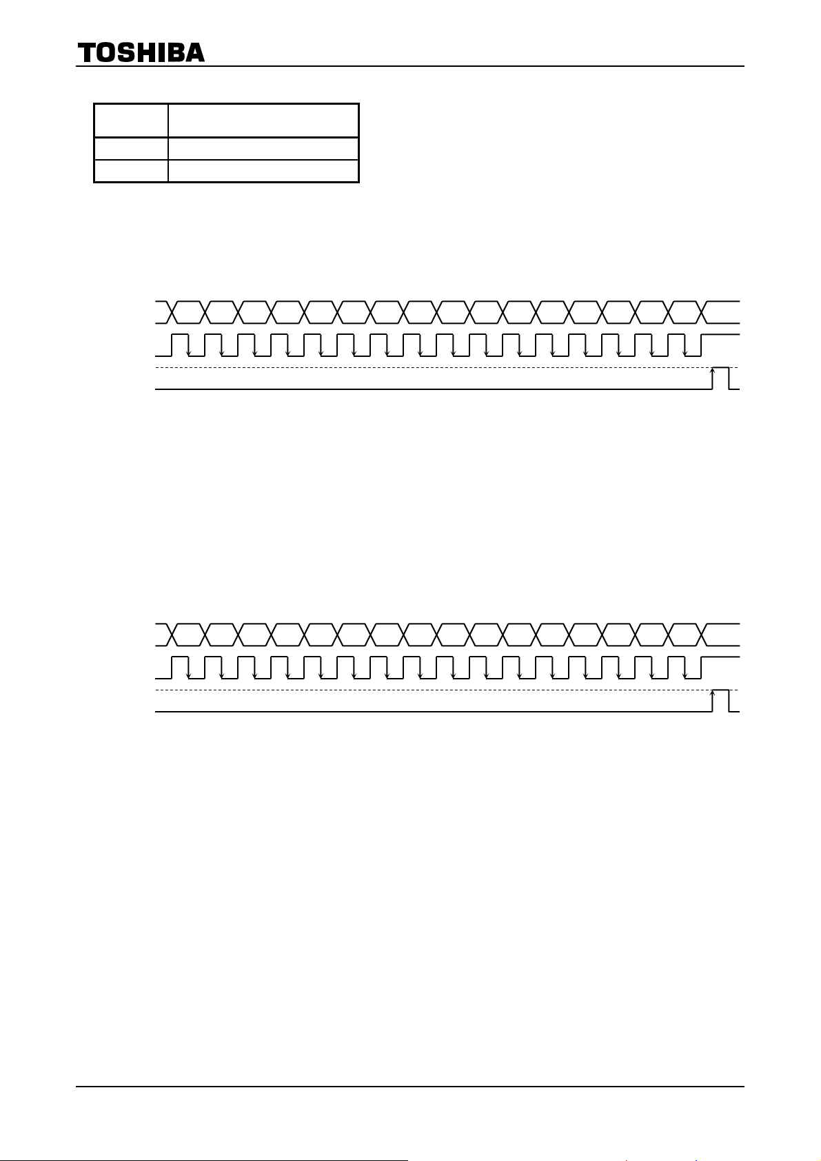
8. Serial Data Input Setting
SETUP pin: L
DATA 0 1 2 3 4 5 6 7 8 9 10 11 12 13 14 15
CLK
STROBE
Note: Data input to the DATA pin are 16-bit serial data.
Data are transferred from DATA 0 (Torque 0) to DATA 15 (Phase A). Data are input and transferred at the
following timings.
At CLK falling edge: data input
At CLK rising edge: data transfer
After data are transferred, all data are latched on the rising edge of the STROBE signal.
As long as STROBE is not rising, the signal can be either Low or High during data transfer.
9. Serial Data Input Setting
(Normal operation)
(Decay timing setup)
SETUP pin: H
DATA 0 1 2 3 4 5 6 7 8 9 10 11 12 13 14 15
CLK
STROBE
Note: Data input to the DATA pin are 16-bit serial data.
• Data are transferred from DATA 0 (Current Mode 1) to DATA 15 (DECAY MODE X-4). Data are input and
transferred at the following timings.
• At CLK falling edge: data input
• At CLK rising edge: data transfer
• After data are transferred, all data are latched on the rising edge of the STROBE signal.
As long as STROBE is not rising, the signal can be either Low or High during data transfer.
13
2005-04-04
Page 14

TB62201AFG
10. Conditions on Overwriting MIXED DECAY TIMING Table
If the following conditions are satisfied, the table can be overwritten.
• When
• When an internal reset is not triggered.
11. Data Input Signal at Setting Mixed Decay Timing Table
Data No. Name Function Initial Value
15 MSB Current Mode 3 Selects Slow or Mixed Decay mode 1 : MIXED DECAY MODE
14 DECAY MODE 3-2 Sets decay 3 ratio (decay 3 raito) 1
13 DECAY MODE 3-1 ↑ 1
12 DECAY MODE 3-0 ↑↑ 1 : 100% : FAST DECAY MODE
11 Current Mode 2 Selects Slow or Mixed Decay mode 1 : MIXED DECAY MODE
10 DECAY MODE 2-2 Sets decay 2 ratio 1
RESET = H (when RESET = L, the shift register is cleared, thus data cannot be input)
1) When the temperature is such that TSD is not triggered (or not reset by TSD).
2) Under a condition where ISD is not triggered (or not reset by ISD).
3) Both V
and VM are within the operating voltage.
DD
Note 1: While the output transistors are operating, do not rewrite the values in the mixed decay timing
table.
Note 2: The SETUP pins is pulled down in the IC by 10-kΩ resistor
When not using the pin, connect it to GND. Otherwise, malfunction may occur.
9 DECAY MODE 2-1 ↑ 0
8 DECAY MODE 2-0 ↑ 1 : 75% MIXED DECAY
7 Current Mode 1 Selects Slow or Mixed Decay mode 1 : MIXED DECAY MODE
6 DECAY MODE 1-2 Sets decay 1 ratio 0
5 DECAY MODE 1-1 ↑ 1
4 DECAY MODE 1-0 ↑ 0 : 37.5% MIXED DECAY
3 Current Mode 0 Selects Slow or Mixed Decay mode 0 : SLOW DECAY MODE
2 DECAY MODE 0-2 Sets decay 0 ratio 0
1 DECAY MODE 0-1 ↑ 0
0 LSB DECAY MODE 0-0 ↑ 0 (SLOW DECAY MODE)
Note 1: Input order of serial data
When setting decay timing, first input H to the SETUP pin, the same as for ordinary data, then
input data from LSB (DATA 0) to MSB (DATA 15).
When power is first turned on, the initial values in the table above are set as defaults.
Once latched, data are not cleared except by VDDR (power-on and power-off reset).
Next, after the mode changes to SETUP, the data are retained until mixed decay timing data are input and
latched.
14
2005-04-04
Page 15

12. Function of Setting Mixed Decay Timing
CURRENT
MODE X
L Don’t care Don’t care Don’t care
H L L L 12.5%
H L L H 25.0%
H L H L 37.5%
H L H H 50.0%
H H L L 62.5%
H H L H 75.0%
H H H L 87.5%
H H H H
Mixed decay timing means the time for switching Slow mode to Fast mode in MIXED DECAY MODE.
In Mixed Decay mode, the Fast mode time at the end of chopping Cycle (T
The IC is switched from Slow to Fast mode according to the percentage representing mode time in the table
above.
(For example, 12.5% means that 12.5% of the time is in Fast mode and the rest of the time, 87.5%, in
Charge and Slow modes.)
Only when the value is maximum (100%), the mode is Fast Decay mode.
DECAY MODE
X-2
DECAY MODE
X-1
DECAY MODE
X-0
MIXED DECAY TIMING
(SLOW DECAY MODE)
(FAST DECAY MODE)
0%
100%
) is fixed by data.
chop
TB62201AFG
15
2005-04-04
Page 16
TB62201AFG
Maximum Ratings
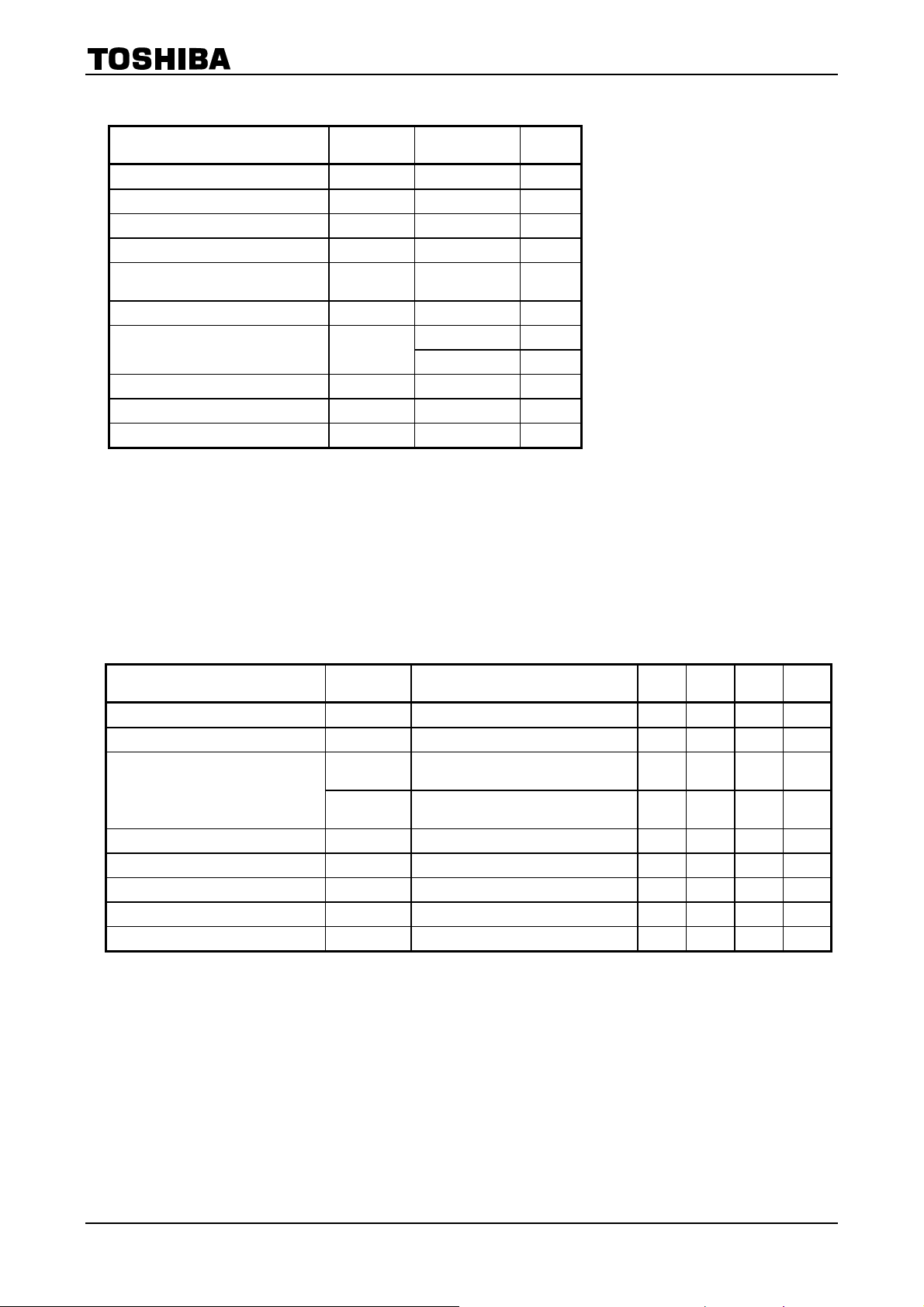
Characteristics Symbol Rating Unit
Logic supply voltage VDD 7 V
Output voltage VM 40 V
Output current I
Current detect pin voltage VRS V
Charge pump pin maximum voltage
(CCP1 pin)
Logic input voltage VIN to VDD + 0.4 V
Power dissipation PD
Operating temperature T
Storage temperature T
Junction temperature Tj 150 °C
(Ta = 25°C)
1.5 A/phase (Note 1)
OUT
± 4.5 V
M
V
V
H
−40 to 85 °C
opr
−50 to 150 °C
stg
+ 7.0 V
M
1.4 W (Note 2)
3.2 W (Note 3)
Note 1: Perform thermal calculations for the maximum current value under normal conditions. Use the IC at 1.2 A or
less per phase.
Note 2: Input 7 V or less as V
.
IN
Note 3: Measured for the IC only. (Ta = 25°C)
Note 4: Measured when mounted on the board. (Ta = 25°C)
Ta: IC ambient temperature
T
: IC ambient temperature when starting operation
opr
T
: IC chip temperature during operation Tj (max) is controlled by TSD (thermal shut down circuit)
j
Recommended Operating Conditions
(Ta = 0 to 85°C)
Characteristics Symbol Test Condition Min Typ. Max Unit
Power supply voltage VDD ⎯ 4.5 5.0 5.5 V
Output voltage VM VDD = 5.0 V 20 24 34 V
= 25°C, per phase
I
OUT (1)
Output current
I
OUT (2)
Logic input voltage VIN ⎯ GND ⎯ VDDV
Clock frequency f
Chopping frequency f
Reference voltage V
Current detect pin voltage VRS VDD = 5.0 V 0 ±1.0 ±1.5 V
CLK
chop
ref
Ta
(when one motor is driven)
= 25°C, per phase
Ta
(when two motors are driven)
VDD = 5.0 V 1.0 6.25 25 MHz
VDD = 5.0 V 40 100 150 kHz
VM = 24 V, T
= 100% 2.0 3.0 V
orque
⎯ 1.1 1.3 A
⎯ 1.1 1.3 A
DD
Note: Use the Maximum Junction Temperature (Tj) at 120°C or less
V
16
2005-04-04
Page 17

Electrical Characteristics 1
(unless otherwise specified, Ta = 25°C, VDD = 5 V, VM = 24 V)
TB62201AFG
Characteristics Symbol
Input voltage
Input current 1
Input current 2
Power dissipation (VDD pin)
Power dissipation (VM pin)
High VIN
Low V
IN (L)
I
IN1 (H)
I
IN1 (L)
I
IN2 (H)
I
IN2 (L)
I
DD1
I
DD2
IM1
IM2
I
Test
Circuit
2.0 VDD
(H)
1 CLK,
⎯ ⎯ 1.0
⎯ ⎯ 700
CLK, STROBE, DATA pins
2
RESET , SETUP pins
V
DD
DATA
Logic, output all off
2
Output OPEN, f
LOGIC ACTIVE, V
Charge Pump
Output OPEN (STROBE,
DATA
Logic, output all off
Charge Pump
3
Output OPEN, f
LOGIC ACTIVE, V
V
M
Charge Pump
Output OPEN, f
LOGIC ACTIVE, 100 kHz
4
M3
chopping (emulation), Output OPEN,
Charge Pump
µF, Ccp2
Test Condition Min Typ. Max Unit
RESET , STROBE, DATA pins
GND
− 0.4
GND 0.8
⎯ ⎯ 1.0
⎯ ⎯ 700
= 5 V (STROBE, RESET ,
= L), RESET = L,
= 6.25 MHz
CLK
= 5 V,
DD
= charged
⎯ 3.0 6.0
⎯ 4.0 80
RESET ,
= L), RESET = L,
⎯ 5.0 6.0
= no operation
= 6.25 MHz
CLK
= 5 V,
= 24 V, Output off
DD
⎯ 12 20
= charged
= 6.25 MHz
CLK
⎯ 30 40
= charged Ccp1 = 0.22
= 0.01µf
V
DD
+ 0.4
V
µA
µA
mA
mA
Output standby
current
Upper I
OH
Output bias current Upper IOB
Output leakage
current
Comparator
Lower I
High
(reference)
Mid high V
OL
V
RS (H)
RS (MH)
reference voltage
ratio
Output current differential ∆I
Output current setting differential ∆I
Mid low V
Low V
RS (ML)
RS (L)
7
out1
7 I
out2
RS pin current IRS 8
V
= VM = 24 V, V
RS
out
= 0 V,
RESET = H, DATA = ALL L
V
= VM = 24 V, V
RS
5
RESET = H, DATA = ALL L
V
= VM = CcpA = V
RS
= 24 V,
out
out
RESET = L
6
= 3.0 V, V
V
ref
TORQUE
= 3.0 V, V
V
ref
TORQUE
= 3.0 V, V
V
ref
TORQUE
= 3.0 V, V
V
ref
TORQUE
(Gain) = 1/5.0
ref
= (H.H) = 100% set
(Gain) = 1/5.0
ref
= (H.L) = 85% set
(Gain) = 1/5.0
ref
= (L.H) = 70% set
(Gain) = 1/5.0
ref
= (L.L) = 50% set
Differences between output current
channels
I
= 1000 mA
out
= 1000 mA −5 ⎯ 5 %
out
= 24 V, V
VRS
(RESET status)
= 24 V, RESET = L
M
=24 V,
−400 ⎯ ⎯
−200 ⎯ ⎯
µA
⎯ ⎯ 1.0
⎯ 100 ⎯
83 85 87
%
68 70 72
48 50 52
−5 ⎯ 5 %
⎯ ⎯ 10 µA
17
2005-04-04
Page 18

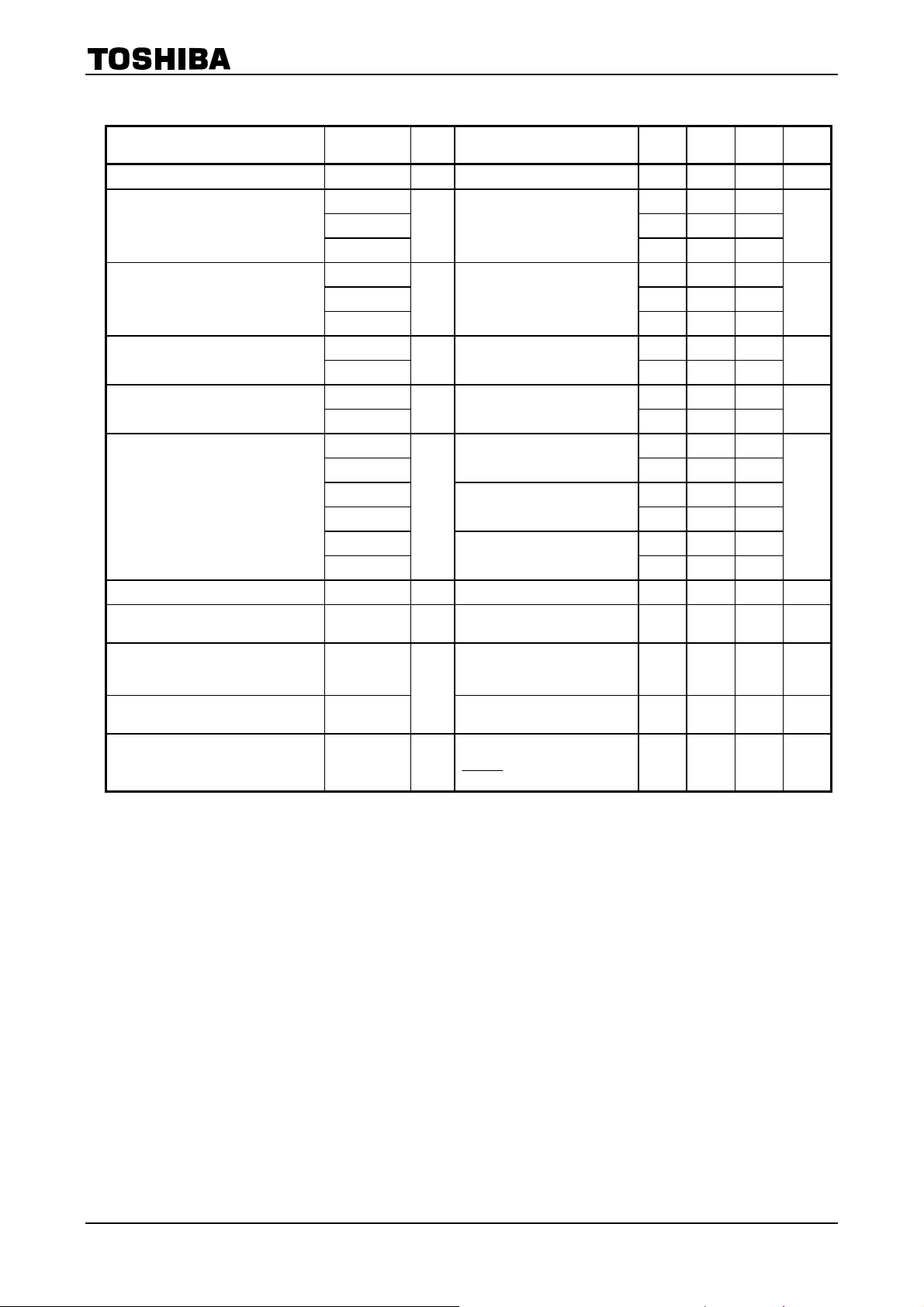
Characteristics Symbol
Output transistor drain-source
on-resistance
R
ON (D-S) 1
R
ON (D-S) 1
R
ON (D-S) 2
R
ON (D-S) 2
Test
Circuit
9
I
out
T
I
out
T
I
out
T
I
out
T
Test Condition Min Typ. Max Unit
= 1.0 A, V
= 25°C, Drain-Source
j
= 1.0 A, VDD = 5.0 V
= 25°C, Source-Drain
j
= 1.0 A, VDD = 5 V,
= 105°C, Drain-Source
j
= 1.0 A, VDD = 5 V,
= 105°C, Source-Drain
j
= 5.0 V
DD
Electrical Characteristics 2
(unless otherwise specified, Ta = 25°C, VDD = 5 V, VM = 24 V)
TB62201AFG
⎯ 0.5 0.6
⎯ 0.5 0.6
Ω
⎯ 0.6 0.75
⎯ 0.6 0.75
Characteristics Symbol
V
input voltage V
ref
V
input current I
ref
V
attenuation ratio V
ref
TSD temperature
TSD return temperature difference ∆TjTSD 11 TjTSD = 130 to 170°C ⎯
VDD return voltage V
VM return voltage VMR 13
Over current protected circuit
operation current
ref
ref
(GAIN) 6
ref
TSD
T
j
(Note 1)
DDR
ISD
(Note 2)
Test
Circuit
V
10
10
12
M
RESET = H, Output on
RESET = H, Output off
V
M
V
ref
V
M
RESET
V
ref
11 V
DD
V
M
STROBE
V
DD
STROBE
VDD = 5 V, VM = 24 V,
14
fchop
Test Condition Min Typ. Max Unit
= 24 V, VDD = 5 V,
= 24 V, VDD = 5 V,
= 3.0 V
= 24 V, VDD = 5 V,
= H, Output on,
= 2.0 to VDD − 1.0 V
= 5 V, VM = 24 V 130 ⎯ 170 °C
= 24 V, RESET = H,
= H
= 5 V,
= H
= 100 kHz set
RESET
= H,
Note 1: Thermal shut down (TSD) circuit
When the IC junction temperature reaches the specified value and the TSD circuit is activated, the internal
reset circuit is activated switching the outputs of both motors to off.
When the temperature is set between 130 (min) to 170°C (max), the TSD circuit operates. When the TSD
circuit is activated, the function data latched at that time are cleared. Output is halted until the reset is
released. While the TSD circuit is in operation, the charge pump is halted.
Even if the TSD circuit is activated and RESET goes H → L → H instantaneously, the IC is not reset until
the IC junction temperature drops 35°C (typ.) below the TSD operating temperature (hysteresis function).
Note 2: Overcurrent protection circuit
When current exceeding the specified value flows to the output, the internal reset circuit is activated
switching the outputs of both shafts to off.
When the ISD circuit is activated, the function data latched at that time are cleared.
Until the RESET signal is input, the overcurrent protection circuit remains activated.
During ISD, the charge pump halts.
For failsafe operation, be sure to add a fuse to the power supply.
2.0
0
1/4.8 1/ 5.0 1/5.2
2.0
2.0
⎯ 2.6 ⎯ A
⎯ V
⎯ 100 A
TSD
T
j
−35
⎯ 4.0 V
⎯ 4.0 V
DD
⎯ °C
V
⎯
18
2005-04-04
Page 19
Electrical Characteristics 3
(Ta = 25°C, VDD = 5 V, VM = 24 V, I
= 1.0 A)
out
TB62201AFG
Characteristics Symbol
Chopper current Vector 15
Test
Circuit
θA = 90 (θ16) ⎯ 100 ⎯
θA = 84 (θ15) ⎯ 100 ⎯
θA = 79 (θ14) 93 98 ⎯
θA = 73 (θ13) 91 96 ⎯
θA = 68 (θ12) 87 92 97
θA = 62 (θ11) 83 88 93
θA = 56 (θ10) 78 83 88
θA = 51 (θ9) 72 77 82
θA = 45 (θ8) 66 71 76
θA = 40 (θ7) 58 63 68
θA = 34 (θ6) 51 56 61
θA = 28 (θ5) 42 47 52
θA = 23 (θ4) 33 38 43
θA = 17 (θ3) 24 29 34
θA = 11 (θ2) 15 20 25
θA = 6 (θ1) 5 10 15
θA = 0 (θ0)
Test Condition Min Typ. Max Unit
⎯
⎯ 0 ⎯
%
19
2005-04-04
Page 20
TB62201AFG
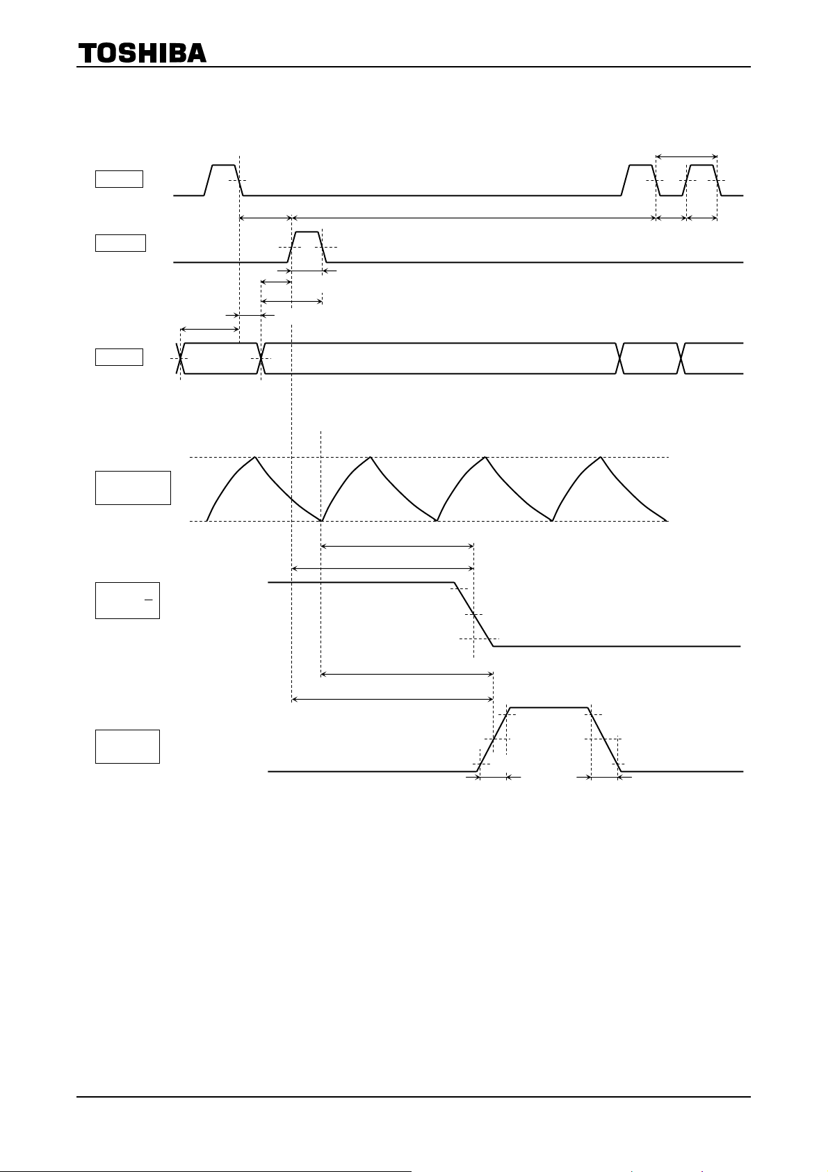
AC Characteristics
(Ta = 25°C, VM = 24 V, VDD = 5 V, 6.8 mH/5.7 Ω)
Characteristics Symbol
Clock frequency f
Minimum clock pulse width
Minimum STROBE pulse width
Data setup time
Data hold time
Output transistor switching
characteristic
Noise rejection dead band time t
CR reference signal oscillation
frequency
Chopping frequency range
Chopping frequency f
Charge pump rise time t
Test
Circuit
16 ⎯ 1.0 ⎯ 25 MHz
CLK
tw
40 ⎯ ⎯
(CLK)
twp
(CLK)
t
wn (CLK)
t
STROBE
t
STROBE (H)
t
STROBE (L)
t
suSIN-CLK
t
suST-CLK
t
Hsin-CLK
t
hCLK-ST
tr ⎯ 0.1 ⎯
16
20 ⎯ ⎯
40 ⎯ ⎯
16 ⎯
16
20 ⎯ ⎯
16
Output Load; 6.8 mH/5.7
tf
t
t
t
t
f
chop (min)
f
chop (typ.)
f
chop (max)
⎯ 15 ⎯
pLH (ST)
pHL (ST)
⎯ 1.2 ⎯
pLH (CR)
pHL (CR)
19 I
BLNK
f
20 C
CR
STROBE (↑) to VOUT
18
Output Load; 6.8 mH/5.7
CR to VOUT
Output Load; 6.8 mH/5.7
Output active (I
Step fixed, Ccp1
Ccp2
20
chop
Output active (I
CR CLK
Ccp2
21
ONG
V
Test Condition Min Typ. Max Unit
⎯
20
⎯ ⎯
20 ⎯ ⎯
20
⎯
20 ⎯ ⎯
20
⎯
20
Ω
Ω
Ω
= 1.0 A 200 300 400 ns
out
= 560 pF, R
osc
= 0.01 µF
= 800 kHz
= 0.22 µF, Ccp = 0.01 µF
= 24 V, VDD = 5 V,
M
= L → H
RESET
= 3.6 kΩ ⎯ 736 ⎯ kHz
osc
= 1.0 A)
out
= 0.22 µF,
= 1.0 A)
out
⎯ 0.1 ⎯
⎯ 10 ⎯
⎯ 2.5 ⎯
40 100 150 kHz
⎯ 100 ⎯ kHz
⎯ 2 4 ms
⎯ ⎯
⎯ ⎯
⎯ ⎯
ns
ns
ns
ns
µs
20
2005-04-04
Page 21
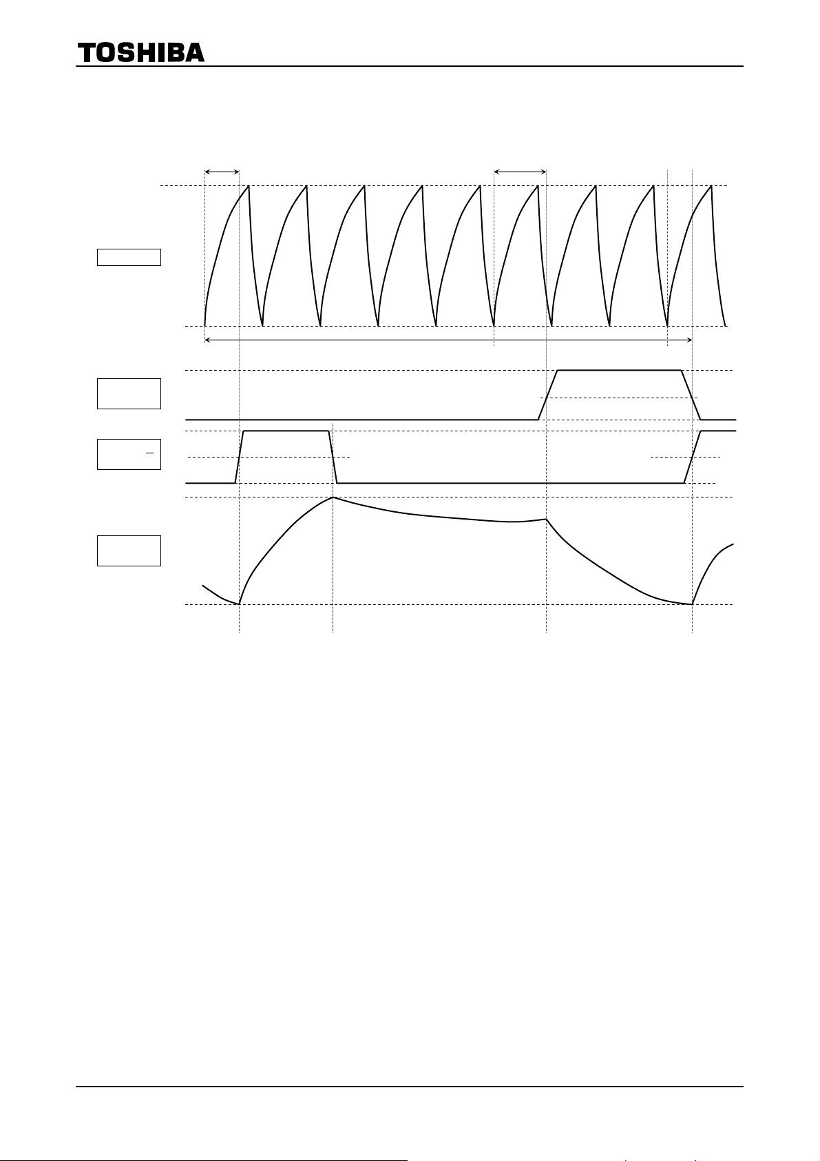
TB62201AFG
Test Waveforms
CLK
STROBE
t
suSIN-CLK
50%
DATA
CR waveform
(reference)
DATA15 DATA0
(Timing waveforms and names)
50%
t
suST-CLK
50%
t
hSIN-CLK
50%
t
STROBE (L)
t
STROBE
t
STROBE (H)
t
hCLK-ST
t
w (CLK)
twn t
wp
OUTPUT
Voltage A
Output
voltage
A
t
pHL (CR)
t
pHL (ST)
t
pLH (CR)
t
pLH (ST)
90%
50%
10%
t
r
10%
50%
90%
90%
50%
10%
tf
21
2005-04-04
Page 22
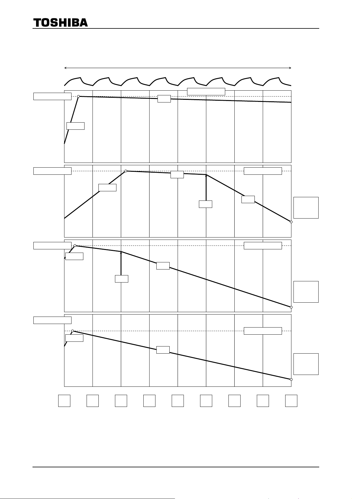
TB62201AFG
Test Waveforms
H
OSC (CR)
L
H
Output
voltage A
L
H
Output
voltage
A
L
Set current
(Timing waveforms and names)
OSC-charge delay
T chop
50%
OSC-fast delay
50%
50%
Output
current
L
Slow Charge
Fast
22
2005-04-04
Page 23

Calculation of Set Current
TB62201AFG
Determining RRS and V
I
(max) =
out
1/5.0 is V
For example,
to input V
R
(gain): V
ref
RS
1
(GAIN) V
ref
= 0.75 Ω (0.5 W or more) is required.
determines the set current value.
ref
=
× V
(V) ×
ref
attenuation ratio (typ.).
ref
= 3 V and Torque = 100% and to output I
ref
orqueorque
R
RS
out
)( )Ω
= 0.8 A,
Formulas for Calculating CR Oscillation Frequency
The CR oscillation frequency and f
1
1
[Hz]
f
KA (constant): 0.523
KB (constant): 600
f
Example: When Cosc = 1,000 pF and Rosc = 2.0 kΩ are connected, f
At this time, the chopping frequency f
Note: fCR =
CR
chop
=
f
CR
=
8
t
CR
can be calculated by the following formulas:
chop
[Hz]
C)KBR(CKA
××××
CR
CR
chop
is: f
= fCR/8 = 92 kHz.
chop
+=
Charge)-(Dis t (Charge) t t
dataserial input :50% 70, 85, 100, (T T
(Chopping reference frequency)
= 735 kHz.
CR oscillation CR charge CR distance
cycle time time
At this time, t (CR − discharge) is subject to the following condition :
600 ns > t (CR − discharge) > 400 ns.
Be sure to set the CR value in accordance with this condition.
23
2005-04-04
Page 24

TB62201AFG
CR Circuit Constants
OSC circuit oscillation waveform
t (CR
− charge) t (CR − dis-charge)
E1
E2
= 0 t = 1 t = 2
t
The OSC circuit generates the chopping reference signal by charging and discharging the external capacitor Cosc
through current supplied from the external resistor Rosc in the OSC block.
Voltages E1 and E2 in the diagram are set by dividing the V
The actual current chopping time is 1/8 the CR frequency.
[Important: Setting the cr circuit constants]
by approximately 3/5 (E1) and 2/5 (E2).
DD
The CR oscillation waveform is converted in the IC to the CLK waveform (CR-CLK signal) and used for control.
If the CR waveform discharge time is set outside the range shown below, the operation of the IC is not guaranteed.
Be sure to set the CR waveform discharge time within the following range.
600 ns > t (CR discharge) > 400 ns
24
2005-04-04
Page 25

TB62201AFG
IC Power Dissipation
IC power dissipation is classified into two: power consumed by transistors in the output block and power consumed
by the logic block and the charge pump circuit.
(1) Power consumed by the Power Transistor (calculated with Ron = 0.6 Ω)
In Charge mode, Fast Decay mode, or Slow Decay mode, power is consumed by the upper and lower transistors
of the H bridges. The following expression expresses the power consumed by the transistors of a H bridge.
P (out) = 2 (T
The average power dissipation for output under 4−bit micro step operation (phase difference between phases A
and B is 90°) is determined by expression (1).
Thus, power dissipation for output per unit is determined as follows (2) under the conditions below.
R
= 0.6 Ω (@ 1.0 A)
on
I
(Peak: max) = 1.0 A
out
V
= 24 V
M
V
= 5 V
DD
P (out) = 2 (T
=1.20 (W)
) × I
r
r
(A) × VDS (V) = 2 × I
out
) × 1.0 (A)^2 × 0.60 (Ω) ................................................................. (2)
^2 × Ron......................................(1)
out
(2) Power consumed by the logic block and IM
The following standard values are used as power dissipation of the logic block and IM at operation.
I (LOGIC) = 2 mA (typ.): /unit
I (IM3) = 12.5 mA (typ.): operation/unit
I (IM1) = 6.0 mA (typ.): stop/unit
The logic block is connected to V
current consumed by output switching) is connected to V
P (Logic & IM) = 5 (V) × 0.002 (A) + 24 (V) × 0.0125 (A).................................... (3)
= 0.31 (W)
(5 V). IM (total of current consumed by the circuits connected to VM and
DD
(24 V). Power dissipation is calculated as follows :
M
(3) Thus, power dissipation for 1 unit (P) is determined as follows by (2) and (3) above.
P = P (out) + P (Logic & IM) = 1.51 (W)
Power dissipation for 1 unit at standby is determined as follows:
P (standby) = 24 (V) × 0.006 (A) + 5 (V) × 0.002 (A)
= 0.154 (W)
When one motor driving = 100 %, power dissipation is determined as follows:
P (all) = 1.51 (W) + 1.664 (W) = 1.66 (W)
For thermal design on the board, evaluate by mounting the IC.
25
2005-04-04
Page 26
TB62201AFG
Mixed Decay Mode Waveforms
CR pin
input
waveform
DECAY MODE 0
SLOW
DECAY
MODE
37.5%
MIXED
DECAY
MODE
NF
Charge
NF
Charge
(concept of mixed decay mode)
f
chop
Set current value
Slow
Slow
MDT
Set current value DECAY MODE 1
Fast
Monitoring
set current
value
RNF
RNF
DECAY MODE 2
75%
MIXED
DECAY
MODE
DECAY MODE 3
FAST
DECAY
MODE
Charge
Charge
100% 75% 50% 25% 0
A B C D E F G H I
NF
Fast
MDT
NF
Fast
87.5% 62.5% 37.5% 12.5%
Set current value
Monitoring
set current
value
RNF
Set current value
Monitoring
set current
value
RNF
In Decay modes 1 to 4, any point from A to H can be set using 3-bit + 1-bit serial data × 4.
(Slow Decay mode for Decay mode 0 in the above figure can be set by setting current Decay mode X to 0.)
NF is the point where the output current reaches the set current value. RNF is the timing for monitoring the set
current.
In Mixed Decay and Fast Decay modes, where the condition RNF (set current monitor signal) < (output current)
applies, Charge mode is cancelled at the next chopping cycle (charge cancel circuit). Therefore, at the next chopping
cycle, the IC enters Slow + Fast modes (Slow → Fast at MDT).
26
2005-04-04
Page 27

Mixed Decay Timing which can be Set
f
Internal
CR
waveform
NF
chop
TB62201AFG
Defaults for
Decay mode 0
0%
12.5%
25%
37.5%
50%
NF
NF
NF
NF
MDT
MDT
MDT
MDT
CURRENT MODE (X)
DECAY MODE (X
X: arbitrary value
CURRENT MODE (X)
DECAY MODE (X
RNF
CURRENT MODE (X)
DECAY MODE (X
RNF
Defaults for
Decay mode 1
CURRENT MODE (X)
DECAY MODE (X
RNF
CURRENT MODE (X)
DECAY MODE (X
= 0
− 2, X − 1, X − 0) = (×, ×, ×)
= 1
− 2, X − 1, X − 0) = (0, 0, 0)
= 1
− 2, X − 1, X − 0) = (0, 0, 1)
= 1
− 2, X − 1, X − 0) = (0, 1, 0)
= 1
− 2, X − 1, X − 0) = (0, 1, 1)
62.5%
75%
87.5%
FAST
DECAY
MODE
NF
NF
MDT
NF
MDT
NF
FAST MODE → RNF: CURRENT MONITOR →
(WHEN SET CURRENT VALUE > OUTPUT CURRENT)
CHARGE MODE → FAST MODE
MDT
RNF
CURRENT MODE (X)
DECAY MODE (X
RNF
Defaults for
Decay mode 2
CURRENT MODE (X)
DECAY MODE (X
RNF
CURRENT MODE (X)
DECAY MODE (X
RNF
Defaults for
Decay mode 3
CURRENT MODE (X)
DECAY MODE (X
RNF
= 1
− 2, X − 1, X − 0) = (1, 0, 0)
= 1
− 2, X − 1, X − 0) = (1, 0, 1)
= 1
− 2, X − 1, X − 0) = (1, 1, 0)
= 1
− 2, X − 1, X − 0) = (1, 1, 1)
27
2005-04-04
Page 28

TB62201AFG
Test Circuit
1. V
IN (H)
5 V
0 V
5 V
0 V
5 V
0 V
No reset at testing
RESET = 5 [V]
VDD
SGND
Test Method
V
IN (H)
V
IN (L)
Setup Data
(A/B unit only. C/D unit conforms to A/B unit.)
, V
IN (L)
osc AB
= 3.6 kΩ
5 V
A
Vary Vin.
I
, I
IN (H)
0 V to 5 V
AB
osc
C
I
DD1
IN (L)
= 560 pF
, I
DD2
A
A
R
SGND
8
CR
27
VDD
31
STROBE AB
30
CLK AB
29
DATA AB
28
RESET
6
SETUP
P-GND
V
ref AB
V
R
RS A
R
RS B
V
V
(FIN)
Ccp C
Ccp B
Ccp A
M A
A
B
M B
SS
9
36
34
A
32
35
B
2
5
3
1
SGND
13
Ccp 2
12
7
0.01 µF
Ccp 1
0.22 µF
: Set RESET to High and vary the logic input voltage from 0 to 7 V.
Monitor I
and measure the change point (VM = 24 V).
DD
: Set RESET to High and vary the logic input voltage from 5 to 0 V.
Monitor I
and measure the change point.
DD
R
R
RS A
RS B
SGND
: PGND
: SGND (V
3 V
SS
24 V
)
DATA
CLK
STROBE
H
L
H
H
0 1 2 3 4 5 6 7 8 9 10 11 12 13 14 15
28
2005-04-04
Page 29

TB62201AFG
2. I
VDD
SGND
IN (H)
I
,
IN (L)
,
I
DD1
, I
(A/B unit only. C/D unit conforms to A/B unit.)
DD2
osc AB
= 3.6 kΩ
A
5 V
0 V
5 V
0 V
5 V
0 V
Vary Vin.
, I
I
IN (H)
0 V to 5 V
No reset at testing
RESET = 5 [V]
5 V
AB
osc
C
I
DD1
IN (L)
= 560 pF
, I
DD2
A
A
R
SGND
8
CR
27
VDD
31
STROBE AB
30
CLK AB
29
DATA AB
28
RESET
6
SETUP
P-GND
V
ref AB
V
R
RS A
A
R
RS B
V
V
(FIN)
Ccp C
Ccp B
Ccp A
M A
B
M B
SS
9
36
34
A
32
35
B
2
5
3
1
13
12
7
SGND
Ccp 2
0.01 µF
Ccp 1
0.22 µF
R
R
RS A
RS B
: PGND
: SGND (V
Test Method
: Set
: Set
RESET
RESET
to High, set the the logic input voltage to 5 V, and measure the input current.
to High, set the the logic input voltage to 0 V, and measure the input current.
I
IN (H)
I
IN (H)
I
: Apply VDD, input RESET, and measure IDD.
DD1
I
: Input 6.25 MHz clock and measure the current when the logic is operating. Set output to OPEN.
DD2
Setup Data
3 V
SGND
SS
24 V
)
DATA
CLK
STROBE
H
L
H
H
0 1 2 3 4 5 6 7 8 9 10 11 12 13 14 15
29
2005-04-04
Page 30

3. IM1, IM2 (A/B unit only. C/D unit conforms to A/B unit.)
osc
= 3.6 kΩ
5 V
0 V
5 V
0 V
5 V
0 V
osc
C
= 560 pF
R
SGND
8
CR AB
27
VDD
31
STROBE AB
30
CLK AB
29
DATA AB
V
ref AB
V
R
R
M A
RS A
A
B
RS B
V
M B
9
36
34
A
32
35
B
2
5
3
1
TB62201AFG
3 V
SGND
VDD
SGND
V
SS
5 V
At IM1 testing: RESET = L (0 V)
At IM2 testing:
5 V
RESET = H (5 V)
28
RESET
P-GND
SETUP
6
(FIN)
Ccp C
Ccp B
Ccp A
13
12
7
SGND
Ccp 2
0.01 µF
Ccp 1
0.22 µF
IM
: PGND
: SGND (V
A
24 V
)
SS
Test Method
IM1: Set the logic block to non-active (DATA = all 0), VDD = 5 V, VM = 24 V, and output to open. Measure
the current input from V
supply.
M
IM2: Set the logic block only to active (CLK = 6.25 MHz), V
current input from V
supply.
M
RESET
RESET
= H
= L
= 24 V, and output to open. Measure the
M
Setup Data
DATA
CLK
H
L
H
0 1 2 3 4 5 6 7 8 9 10 11 12 13 14 15
STROBE
H
30
2005-04-04
Page 31

4. IM3 (A/B unit only. C/D unit conforms to A/B unit.)
osc AB
= 3.6 kΩ
5 V
0 V
5 V
0 V
5 V
0 V
osc AB
= 560 pF
C
R
SGND
8
CR AB
27
VDD
31
STROBE AB
30
CLK AB
29
DATA AB
V
ref AB
V
R
R
M A
RS A
A
B
RS B
V
M B
TB62201AFG
9
3 V
36
34
A
32
35
B
2
5
3
1
SGND
28
RESET
5 V
VDD
SGND
5 V
No reset at testing
RESET = 5 [V]
P-GND
SETUP
6
This is the IM current when all of the circuits, including the output transistors, in the IC are operating.
The IM current includes the current dissipation in the charge pump circuit, output gate loss, and output
predriver.
Because the IM current (IM3) is input from the RS pin, which is also used for the output current, IM3
cannot be measured by the normal testing methods.
Use the method shown below.
Setup Data
The serial data PHASE signal (both A and B) switch over to high or low.
DATA
CLK
H
L
H
0 1 2 3 4 5 6 7 8 9 10 11 12 13 14 15
V
SS
(FIN)
Ccp C
Ccp B
Ccp A
13
12
SGND
Ccp 2
0.01 µF
7
Ccp 1
0.22 µF
: PGND
: SGND (V
A
IM
24 V
)
SS
STROBE
H
Test Method
Set output to open, change phase data from 1 → 0 → 1 → 0 and perform switching. When testing, input
phase data at double the chopping frequency (if f
current value of V
supply.
M
fDATA = 200 kHz means that the phase switches at 200 kHz.
= 100 kHz, fDATA = 200 kHz) and measure the
chop
31
2005-04-04
Page 32

TB62201AFG
Number of Switchings at Phase Switching Number of Switchings at Actual Operation
Mode changes three times
in one chopping cycle.
To VM
RS
R
One phase switching
(16-bit data input)
Four transistors switching
To V
RS
R
M
Chopping cycle
U1
ON
Load
L1
OFF
PGND
Four transistors are switched at one phase switching
U2
OFF
Switches by phase data
L2
ON
Four transistors switching
One phase switching
(16-bit data input)
U1 U
OFF
L1 L
ON
Load
PGND
ON
OFF
2
2
ON
OFF
Charge
Four transistors switching
Eight transistors switching
in one chopping cycle
OFF
Two transistors
switching
ON
ON ON
OFF
ON
Slow
Fast
Number of switchings at actual operation = 2 × number of switchings at phase switching.
Therefore, switching the phase at 2 × chopping cycle matches the number of switchings at actual operation
with the number of switchings at phase switching, and allows the actual current dissipation, IM3, to be
measured.
OFFOFF
Two transistors
switching
ON
OFF
32
2005-04-04
Page 33

TB62201AFG
5. IOB, IOH, IOL
VDD
SGND
Test Method
IOH: With VM = 24 V, VDD = 5 V, and logic input all = 0 applied, set
to GND, and measure the supply current.
I
: With VM = 24 V, VDD = 5 V, and logic input all = 0 applied, set
OB
to V
I
: With VM = 24 V, VDD = 5 V, and logic input all = 0 applied, set
OL
to GND, and measure the supply current.
Setup Data
(A/B unit only. C/D unit conforms to A/B unit.)
osc
= 3.6 kΩ
R
osc AB
SGND
= 560 pF
C
5 V
0 V
5 V
0 V
5 V
0 V
5 V
5 V
M
No reset at testing
RESET = 5 [V]
, and measure the supply current.
IOL
8
CR AB
27
VDD
31
STROBE AB
30
CLK AB
29
DATA AB
28
RESET
P-GND
SETUP
6
V
ref AB
V
M A
R
RS A
A
R
RS B
V
V
(FIN)
Ccp C
Ccp B
Ccp A
B
M B
SS
9
3 V
36
34
A
32
35
B
2
5
3
1
13
12
7
RESET
RESET
RESET
A
IOB
IOH, IOL
A
SGND
Ccp 2
0.01 µF
Ccp 1
0.22 µF
= H, connect the output pins
= H, connect the output pins
= L, connect the output pins
SGND
: PGND
: SGND (V
SS
24 V
)
DATA
CLK
STROBE
H
L
H
H
0 1 2 3 4 5 6 7 8 9 10 11 12 13 14 15
33
2005-04-04
Page 34

TB62201AFG
6. VRS (H to L), V
(A/B unit only. C/D unit conforms to A/B unit.)
VDD
SGND
V
RS (H to L):
V
ref (GAIN)
(GAIN) (when measuring phase A) after Measurement
ref
osc AB
= 3.6 kΩ
R
5 V
0 V
5 V
0 V
5 V
0 V
5 V
AB
osc
SGND
C
= 560 pF
5 V
No reset at testing
RESET = 5 [V]
8
CR AB
27
VDD
31
STROBE AB
30
CLK AB
29
DATA AB
28
RESET
P-GND
SETUP
6
Input torque data = 100% (HH) and vary the voltage between VM and RS pins.
Measure the voltage (V
Also measure V
when torque data = 85% (HL), 70% (LH), or 50% (LL) as above and
RS
calculate the ratio using V
(*) V
: V
ref (GAIN)
RS
=
V
ref
) when output changes from fixed Charge mode to another mode.
RS
value at 100% as reference.
RS
((*) VRS: when torque data = 100%)
V
ref AB
V
R
RS A
A
R
RS B
V
V
(FIN)
Ccp C
Ccp B
Ccp A
M A
B
M B
SS
9
36
34
A
32
35
B
2
5
3
1
13
12
7
Oscilloscope
Vary between
0 and 1 V.
SGND
Ccp 2
0.01 µF
Ccp 1
0.22 µF
SGND
V
: PGND
: SGND (V
3 V
SS
24 V
)
Setup Data
DATA
CLK
STROBE
H
L
H
H
0 1 2 3 4 5 6 7 8 9 10 11 12 13 14 15
34
2005-04-04
Page 35

7.
TB62201AFG
∆
I
out1
, ∆I
5 V
0 V
5 V
0 V
5 V
0 V
(A/B unit only. C/D unit conforms to A/B unit.)
out2
osc
= 3.6 kΩ
C
osc
= 560 pF
R
SGND
8
CR
27
VDD
31
STROBE AB
30
CLK AB
29
DATA AB
V
ref AB
V
R
RS A
A
R
RS B
V
M A
B
M B
9
3 V
36
34
A
32
35
B
2
5
3
1
R
R
RS A
RS B
Monitors current
SGND
waveform.
V
SS
VDD
SGND
5 V
5 V
No reset at testing
RESET = 5 [V]
28
RESET
P-GND
SETUP
6
(FIN)
Ccp C
Ccp B
Ccp A
13
12
7
SGND
Ccp 2
0.01 µF
Ccp 1
0.22 µF
: PGND
: SGND (V
SS
)
With L load, perform chopping in Mixed Decay mode. Monitor the output current waveform and measure
the various output currents at constant current operation.
Setup Data
Set to 100%
DATA
CLK
STROBE
H
L
H
H
0 1 2 3 4 5 6 7 8 9 10 11 12 13 14 15
24 V
waveform
Current
Output current
value (set
current value)
0%
Charge
Slow
MDT
Fast
35
0%100%
Charge
Slow
MDT
Fast
Measurement of
peak current
2005-04-04
Page 36

TB62201AFG
8. IRS (when measuring phase A) (A/B unit only. C/D unit conforms to A/B unit)
osc
= 3.6 kΩ
C
osc
= 560 pF
R
SGND
8
CR AB
27
VDD
31
STROBE AB
30
CLK AB
29
DATA AB
V
ref AB
V
R
R
M A
RS A
A
B
RS B
V
M B
9
36
34
A
32
35
B
2
5
3
1
A
3 V
SGND
V
SS
28
RESET
RESET = L
VDD
SGND
With L input to
R
S
5 V
RESET
, connect VM and RRS to the power supply, and measure the current input to the
P-GND
SETUP
6
pin. (Either drop all the input pins to GND level or input all Low data to the DATA pin, then perform
(FIN)
Ccp C
Ccp B
Ccp A
13
12
7
SGND
Ccp 2
0.01 µF
Ccp 1
0.22 µF
: PGND
: SGND (V
measurement. At that time, leave all other output pins open.)
Setup Data
DATA
CLK
STROBE
H
L
H
H
0 1 2 3 4 5 6 7 8 9 10 11 12 13 14 15
SS
24 V
)
36
2005-04-04
Page 37

TB62201AFG
9. R
R
ON (D-S)
,
ON (S-D)
(A/B unit only. C/D unit conforms to A/B unit.)
5 V
0 V
5 V
0 V
5 V
0 V
SGND
5 V
when Measuring Output A
osc
= 3.6 kΩ
R
osc
SGND
= 560 pF
C
5 V
No reset at testing
RESET = 5 [V]
8
CR AB
27
VDD
31
STROBE AB
30
CLK AB
29
DATA AB
28
RESET
P-GND
SETUP
6
V
ref AB
V
M A
R
RS A
A
B
R
RS B
V
M B
V
SS
(FIN)
Ccp C
Ccp B
Ccp A
9
3 V
36
34
A
32
35
B
2
5
3
1
13
12
7
Curve tracer
Curve tracer
SGND
Ccp 2
0.01 µF
Ccp 1
0.22 µF
SGND
: PGND
: SGND (V
SS
24 V
)
Input the current setting data (HHHH signal) to the DATA pin and measure the voltage between VM and
OUT when I
= 1000 mA or the voltage between OUT and GND. Then, change the phase and repeat
out
measurement. At that time, leave the output pins which are not measured open.
Setup Data
(Vary the phase data during testing.)
DATA
CLK
STROBE
H
L
H
H
0 1 2 3 4 5 6 7 8 9 10 11 12 13 14 15
37
2005-04-04
Page 38

TB62201AFG
10. V
VDD
SGND
, I
(A/B unit only. C/D unit conforms to A/B unit.)
ref
osc AB
= 3.6 kΩ
R
5 V
: Vary V
osc AB
SGND
= 560 pF
C
5 V
No reset at testing
RESET = 5 [V]
= 2 to VDD − 1 V and confirm that output is on.
ref
8
CR AB
27
VDD
31
STROBE AB
30
CLK AB
29
DATA AB
28
RESET
P-GND
SETUP
6
: When VM = 24 V and VDD = 5 V, apply the specified voltage of 3 V to the V
V
I
ref
ref
ref
V
ref AB
V
R
RS A
A
R
RS B
V
V
(FIN)
Ccp C
Ccp B
Ccp A
M A
B
M B
SS
9
36
34
A
32
35
B
2
5
3
1
13
12
7
Oscilloscope
current flow value.
Monitor
A
I
(*)
ref
R
SGND
Ccp 2
0.01 µF
Ccp 1
0.22 µF
(*) When measuring I
fix V
measure.
Vary V
= 2 to V
RS A
: PGND
: SGND (V
and monitor the
ref
ref
DD
= 3 V and
ref
− 1.0 V
SS
24 V
)
ref
SGND
,
38
2005-04-04
Page 39

TB62201AFG
11. TjTSD, ∆TjTSD
the temperature for the IC can be freely changed) (A/B unit only. C/D unit conforms to A/B
unit.)
5 V
0 V
5 V
0 V
5 V
0 V
SGND
T
TSD : Increase the ambient temperature. Measure the temperature when output stops.
j
∆T
Setup Data
5 V
TSD : Gradually lower the temperature from the level when the TSD circuit was operating (output off).
j
At that time, control the RESET input thus : H → L → H → L. Output will begin at a certain
temperature level.
∆T
which TSD is triggered.
(Measure in an environment such as an constant temperature chamber where
osc
= 3.6 kΩ
R
osc
SGND
= 560 pF
C
5 V
No reset at testing
RESET = 5 [V]
TSD is the difference between the temperature at which output begins and the temperature at
j
8
CR AB
27
VDD
31
STROBE AB
30
CLK AB
29
DATA AB
28
RESET
P-GND
SETUP
6
V
ref AB
V
R
RS A
A
R
RS B
V
V
(FIN)
Ccp C
Ccp B
Ccp A
M A
B
M B
SS
9
3 V
36
34
A
32
35
B
2
5
3
1
13
12
7
Curve tracer
Curve tracer
SGND
Ccp 2
0.01 µF
Ccp 1
0.22 µF
SGND
: PGND
: SGND (V
SS
24 V
)
DATA
CLK
STROBE
H
L
H
H
0 1 2 3 4 5 6 7 8 9 10 11 12 13 14 15
39
2005-04-04
Page 40

TB62201AFG
12. V
DDR
VDD
SGND
VDD
SGND
(A/B unit only. C/D unit conforms to A/B unit.)
osc
= 3.6 kΩ
R
5 V
5 V
0 V
5 V
0 V
5 V
0 V
Vary from 0 V.
osc
C
No reset at testing
RESET = 5 [V]
= 560 pF
SGND
5 V
8
CR AB
27
VDD
31
STROBE AB
30
CLK AB
29
DATA AB
28
RESET
P-GND
SETUP
6
V
ref AB
V
R
RS A
A
R
RS B
V
V
(FIN)
Ccp C
Ccp B
Ccp A
M A
B
M B
SS
9
36
34
A
32
35
B
2
5
3
1
13
12
7
Oscilloscope
R
RS A
R
RS B
SGND
Ccp 2
0.01 µF
Ccp 1
0.22 µF
SGND
V
M
: PGND
: SGND (V
3 V
SS
24 V
)
Monitor the output pins. Increase the VDD voltage from 0. Measure the VDD value when output starts.
Next, decrease the V
voltage and measure the VDD value when output stops.
DD
Setup Data
DATA
CLK
STROBE
H
L
H
H
0 1 2 3 4 5 6 7 8 9 10 11 12 13 14 15
40
2005-04-04
Page 41

TB62201AFG
13. VMR
(A/B unit only. C/D unit conforms to A/B unit.)
A
B
SS
Oscilloscope
9
36
34
32
35
2
5
3
1
13
12
7
R
R
SGND
Ccp 2
0.01 µF
Ccp 1
0.22 µF
VDD
SGND
5 V
0 V
5 V
0 V
5 V
0 V
5 V
osc
= 3.6 kΩ
R
osc
SGND
= 560 pF
C
5 V
No reset at testing
RESET = 5 [V]
8
CR AB
27
VDD
31
STROBE AB
30
CLK AB
29
DATA AB
28
RESET
P-GND
SETUP
6
V
ref AB
V
R
RS A
A
R
RS B
V
V
(FIN)
Ccp C
Ccp B
Ccp A
M A
B
M B
With the CLK signal and DATA (all High) input, increase the VM voltage from 0.
Measure the V
Next, decrease the V
value when output starts.
M
voltage and measure the VM value when output stops.
M
Setup data
RS A
RS B
Vary from 0 V.
SGND
: PGND
: SGND (V
3 V
SS
)
DATA
CLK
STROBE
H
L
H
H
0 1 2 3 4 5 6 7 8 9 10 11 12 13 14 15
41
2005-04-04
Page 42

TB62201AFG
14. Overcurrent Protector Circuit
(A/B unit only. C/D unit conforms to A/B unit.)
osc AB
R
SGND
= 560 pF
5 V
, increase the current flow. There is a current value at which output is switched off
AB
osc
C
5 V
0 V
5 V
0 V
5 V
0 V
SGND
At measuring, non-reset
5 V
RESET = 5 [V]
Test method: To monitor operating current of the overcurrent protector circuit when output A is
short-circuited to the power supply
Input the current setting data (HHHH signal) to the DATA pin. If short-circuited to the supply, measure
the lower output transistors. If short-circuited to ground, measure the upper output transistors (see how to
measure R
When measuring R
and R
ON
).
ON
ON
cannot be measured. This value is the set current value for the overcurrent protector circuit.
Make sure to leave open the output pins not being measured.
Note that if the temperature changes, the value may fluctuate. Try to avoid applying power to the IC by
one-shot measuring.
Setup Data
(Example: The phase signal must be changed depending on the pin.)
(ISD) (To measure output A: )
= 3.6 kΩ
8
CR AB
27
VDD
31
STROBE AB
30
CLK AB
29
DATA AB
28
RESET
P-GND
SETUP
6
V
ref AB
V
R
RS A
A
R
RS B
V
V
(FIN)
Ccp C
Ccp B
Ccp A
M A
B
M B
SS
9
3 V
36
34
A
32
35
B
2
5
3
1
13
12
7
Curve tracer
Curve tracer
SGND
Ccp 2
0.01 µF
Ccp 1
0.22 µF
SGND
: PGND
: SGND (V
SS
24 V
)
DATA
CLK
STROBE
H
L
H
H
0 1 2 3 4 5 6 7 8 9 10 11 12 13 14 15
42
2005-04-04
Page 43

TB62201AFG
15. Current Vector
5 V
0 V
5 V
0 V
5 V
0 V
VDD
SGND
Perform chopping in Mixed Decay mode with load L. Monitor the output current waveform and measure
the output current at constant current operation. At this time, vary the 4-bit data for current setting and
measure the current values. Using the set output current as 100%, calculate the output current ratio.
5 V
(A/B unit only. C/D unit conforms to A/B unit.)
osc
= 3.6 kΩ
R
osc
SGND
= 560 pF
C
5 V
At measuring, non-reset
RESET = 5 [V]
8
CR
27
VDD
31
STROBE AB
30
CLK AB
29
DATA AB
28
RESET
P-GND
SETUP
6
V
R
R
Ccp C
Ccp B
Ccp A
ref AB
V
M A
RS A
A
B
RS B
V
M B
V
SS
(FIN)
9
3 V
36
34
A
32
35
B
2
5
3
1
13
12
7
SGND
Ccp 2
0.01 µF
Ccp 1
0.22 µF
R
R
RS A
RS B
Monitor current
SGND
waveform
: PGND
: SGND (V
SS
24 V
)
100%
Output current
(example)
71%
100%
0%
43
2005-04-04
Page 44

TB62201AFG
16. f
, t
CLK
w (CLK)
t
suSIN-CLK
VDD
SGND
Input any data at f
, t
5 V
0 V
5 V
0 V
5 V
0 V
5 V
, t
wp (CLK)
suST-CLK
osc
= 560 pF
C
5 V
No reset at testing
RESET = 5 [V]
(max), perform chopping, and monitor the output waveform.
CLK
t
,
wn (CLK)
, t
hSIN-CLK
osc
= 3.6 kΩ
R
SGND
, t
, t
hCLK-ST
8
CR AB
27
VDD
31
STROBE AB
30
CLK AB
29
DATA AB
28
RESET
P-GND
STROBE
SETUP
6
For the measuring points, see the timing chart below.
Setup Data
, t
STROBE (H)
, t
STOBE (L)
,
(A/B unit only. C/D unit conforms to A / B unit.)
V
ref AB
V
M A
R
RS A
A
B
R
RS B
V
M B
V
SS
(FIN)
Ccp C
Ccp B
Ccp A
9
36
34
A
32
35
B
2
5
3
1
13
12
7
SGND
Ccp 2
0.01 µF
Ccp 1
0.22 µF
R
R
RS A
RS B
: PGND
: SGND (V
3 V
SGND
SS
24 V
)
DATA
CLK
STROBE
Measuring Points
CLK
STROBE
DATA
H
L
H
H
0 1 2 3 4 5 6 7 8 9 10 11 12 13 14 15
50%
t
t
suSIN-CLK
50%
DATA15
suST-CLK
50%
50%
t
STROBE (L)
t
hIN-CLK
t
STROBE (H)
t
STROBE
t
hST-CLK
t
wn (CLK) twp (CLK)
DATA0
44
t
w (CLK)
2005-04-04
Page 45

TB62201AFG
17. OSC-fast Delay, OSC-charge Delay
osc
= 3.6 kΩ
R
osc
SGND
= 560 pF
C
5 V
0 V
5 V
0 V
5 V
0 V
5 V
VDD
SGND
5 V
No reset at testing
RESET = 5 [V]
Fix the output current value in Mixed Decay mode and turn the output on. Measure the time until the
output switches from the CR pin waveform and the output voltage waveform.
Setup Data
8
27
31
30
29
28
(A/B unit only. C/D unit conforms to A / B unit.)
CR AB
VDD
STROBE AB
CLK AB
DATA AB
RESET
P-GND
SETUP
V
6
ref AB
V
M A
R
RS A
A
B
R
RS B
V
M B
V
SS
(FIN)
Ccp C
Ccp B
Ccp A
9
36
34
A
32
35
B
2
5
3
1
13
12
7
SGND
Ccp 2
0.01 µF
Ccp 1
0.22 µF
R
R
RS A
RS B
SGND
: PGND
: SGND (V
3 V
SS
24 V
)
Top
CR
Bottom
V
out A
V
out A
(Mode)
DATA
CLK
STROBE
H
L
H
H
50%
0 1 2 3 4 5 6 7 8 9 10 11 12 13 14 15
Osc-charge delay Osc-fast delay
50%
50%
SlowCharge Fast Charge
45
50% 50%
2005-04-04
50%
Page 46

TB62201AFG
rtf
18. t
pHL (ST)
5 V
0 V
5 V
0 V
5 V
0 V
VDD
SGND
Setup Data
, t
pLH (ST)
5 V
, tr, t
(A/B unit only. C/D unit conforms to A/B unit.)
f
osc
= 3.6 kΩ
R
osc
SGND
= 560 pF
C
5 V
No reset at testing
RESET = 5 [V]
8
CR AB
27
VDD
31
STROBE AB
30
CLK AB
29
DATA AB
28
RESET
P-GND
SETUP
6
Monitor
V
9
ref AB
V
M A
R
RS A
A
B
R
RS B
V
M B
V
SS
(FIN)
Ccp C
Ccp B
Ccp A
36
34
A
32
35
B
2
5
3
1
13
12
7
SGND
Ccp 2
0.01 µF
Ccp 1
0.22 µF
R
RS A
L = 6.8 mH
R
RS B
RL = 5.7 Ω
: PGND
: SGND (V
3 V
SGND
SS
24 V
)
DATA
CLK
STROBE
H
L
H
H
0 1 2 3 4 5 6 7 8 9 10 11 12 13 14 15
Switch PHASE every 130 µs and measure the output pin voltage and the STROBE signal.
[Oscilloscope Waveform (example)]
STROBE
Output
voltage
Output
voltage A
A
50%
t
pHL (ST)
t
pLH (ST)
130 µs
50%
90% 90%
50%
10% 10%
t
50%
46
2005-04-04
Page 47

TB62201AFG
19. t
BRANK
(A/B unit only. C/D unit conforms to A/B unit.)
osc AB
= 3.6 kΩ
5 V
0 V
5 V
0 V
5 V
0 V
5 V
SGND
t
BRANK
is the dead time band for avoiding malfunction caused by noise. Apply sufficient differential
voltage (when V
R
osc AB
SGND
= 560 pF
C
5 V
No reset at testing
RESET = 5 [V]
= 3 V, 0.6 V or higher) to VM-RS and apply duty. When the pulse width reaches a certain
ref
8
CR AB
27
V
DD AB
31
STROBE AB
30
CLK AB
29
DATA AB
28
RESET
P-GND
SETUP
6
V
ref AB
R
R
Ccp C
Ccp B
Ccp A
value, triggering feedback and changing the output. Check the value.
V
M A
RS A
A
B
RS B
V
M B
V
(FIN)
SS
9
3 V
36
34
A
32
35
B
2
5
3
1
13
12
7
SGND
Ccp 2
0.01 µF
Ccp 1
0.22 µF
R
R
RS A
RS B
SGND
: PGND
: SGND (V
SS
24 V
)
RS pin voltage
Output operation
Setup Data
DATA
CLK
STROBE
Measure the pulse width
V
M
Apply pulse to the RS pin
so that the R
= V
voltage − 1.0 V.
H
L
M
pin
S
where output changes.
H
L
H
H
0 1 2 3 4 5 6 7 8 9 10 11 12 13 14 15
47
2005-04-04
Page 48

TB62201AFG
20. f
chop
(f
chop
(min), f
VDD
SGND
Change the R
5 V
osc
and C
At this time, 1/8 of the frequency of the measured CR waveform is f
Oscilloscope Waveform
osc AB
= 560 pF
C
c
(max)) (A/B unit only. C/D unit conforms to A/B unit.)
hop
Oscilloscope
osc AB
= 3.6 kΩ
R
8
CR AB
SGND
27
VDD
31
STROBE AB
30
CLK AB
29
DATA AB
28
RESET
P-GND
values and measure the frequency on the CR pin using the oscilloscope.
osc
SETUP
6
V
ref AB
V
R
RS A
A
R
RS B
V
V
(FIN)
Ccp C
Ccp B
Ccp A
M A
B
M B
SS
9
36
34
A
32
35
B
2
5
3
1
13
12
7
chop
SGND
Ccp 2
0.01 µF
Ccp 1
0.22 µF
.
R
R
RS A
RS B
: PGND
: SGND (V
(example)
3 V
SGND
SS
24 V
)
1/8 f
t = 0 t = 1
(SYNC) = f
chop
CR
48
2005-04-04
Page 49

TB62201AFG
21. t
VDD
SGND
(A/B unit only. C/D unit conforms to A/B unit.)
ONG
osc
= 3.6 kΩ
R
Apply V
osc
SGND
= 560 pF
C
5 V
0 V
5 V
0 V
5 V
0 V
5 V
At measuring, change
5 V
from reset to non-reset.
and VDD and change RESET from L to H.
M
8
27
31
30
29
28
Measure the time until the CcpA pin becomes V
CR AB
V
DD
STROBE AB
CLK AB
DATA AB
RESET
P-GND
SETUP
V
ref AB
R
R
Ccp C
Ccp B
Ccp A
6
+ VDD × 90%.
M
V
M A
RS A
A
B
RS B
V
M B
V
(FIN)
SS
9
3 V
36
34
A
32
35
B
2
5
3
1
13
12
7
SGND
Ccp 2
0.01 µF
Ccp 1
0.22 µF
R
R
RS A
RS B
SGND
: PGND
: SGND (V
SS
24 V
)
V
+ VM
DD
+ VDD) × 90%
(V
M
V
M
RESET
5 V
0 V
50%
t
ONG
49
2005-04-04
Page 50

TB62201AFG
22. Mixed Decay Timing
osc
= 560 pF
C
5 V
0 V
5 V
0 V
5 V
0 V
At measuring, non-reset
VDD
SGND
When overwriting the
mixed decay timing
table, set to 5 V.
When the motors are
operating, set to
GND level.
RESET = 5 [V]
5 V
(A/B unit only. C/D unit conforms to A/B unit.)
osc
= 3.6 kΩ
R
SGND
5 V
5 V
8
CR
27
V
DD
31
STROBE AB
30
CLK AB
29
DATA AB
28
RESET
6
SETUP
P-GND
V
ref AB
V
R
RS A
A
R
RS B
V
V
(FIN)
Ccp C
Ccp B
Ccp A
M A
B
M B
SS
9
36
34
A
32
35
B
2
5
3
1
SGND
13
Ccp 2
12
7
0.01 µF
Ccp 1
0.22 µF
R
R
RS A
RS B
SGND
: PGND
: SGND (V
3 V
SS
24 V
)
With V
= 24 V, VDD = 5 V, RESET = H, change the SETUP pin from L to H and overwrite the MIXED
M
DECAY TIMING TABLE.
Then change the SETUP pin from H to L. With load L, perform chopping and monitor the output current
waveform at that time. Confirm that the switching timing from Slow Decay Mode to Fast Decay Mode
within an fchop cycle is the specified MIXED DECAY TIMING.
(Depending on the load L value and the test environment, chopping may be performed every two cycles or
there may be no Slow Decay Mode. If so, conditions, for example, load condition, may need to be changed.
Output current value
(set current value)
Charge
Slow
MDT 100% 0% MDT 0%
Slow Fast
Charge
Current waveform
MDT MDT
Fast
50
2005-04-04
Page 51

TB62201AFG
Waveforms in Various Current Modes
Normal MIXED DECAY MODE Waveform
f
f
chop
CR CLK
signal
I
out
Set current value
Set current
value
12.5% MIXED
DECAY MODE
When NF is after MIXED DECAY TIMING
NF
MDT (MIXED DECAY TIMING) point
(Ideal waveform)
NF is the point at which the output current
reaches the set current value.
RNF
chop
NF
Fast Decay mode after Charge mode.
I
out
Set current
value
37.5% MIXED
DECAY MODE
NF
STROBE signal input
Set current value
MDT (MIXED DECAY TIMING) point
RNF
NF
RNF
51
2005-04-04
Page 52

In MIXED DECAY MODE, when the Output Current > the Set Current Value
TB62201AFG
f
chop
Set
current
value
I
out
12.5%
MIXED
DECAY
MODE
NF
STROBE signal input
FAST DECAY MODE Waveform
f
chop
CHARGE MODE for one f
cycle after STROBE signal input
RNF
NF
Set current value
MDT (MIXED DECAY TIMING) point
f
chop
RNF
chop
f
chop
Because the set current value >
the output current, no CHARGE
MODE in the next cycle.
NF
RNF
f
chop
NF is the point at which the output
current reaches the set current value.
Set current
value
I
out
FAST DECAY
MODE
(0% MIXED
DECAY MODE)
Because the set current value > the output current,
FAST DECAY MODE in the next cycle, too
RNF
Because the set current value > the output current, CHARGE
→ NF → FAST DECAY MODE in the next cycle, too
MODE
Set current value
NF
RNF
RNF
STROBE signal input
Response delay time
52
2005-04-04
Page 53

STROBE Signal, Internal CR CLK, and Output Current Waveform
(When STROBE signal is input in SLOW DECAY MODE)
TB62201AFG
Set current
value
I
out
STROBE signal input
When STROBE signal is input, the chopping counter (CR-CLK counter) is forced to reset at the next
CR-CLK timing.
Because of this, compared with a method in which the counter is not reset, response to the input data is
faster.
(The delay time, the theoretical value in the logic portion, is expected to be a one-cycle CR waveform:
1.25 µs @ 100 kHz CHOPPING.)
When the C-CLK counter is reset due to STROBE signal input, CHARGE MODE is entered momentarily
due to current comparison.
f
chop
Set current
value
Reset CR-CLK
counter here
f
chop
MDT
f
37.5% MIXED DECAY MODE
NF
RNF
Momentarily enters
CHARGE MODE
chop
MDT
RNF
Note: In FAST DECAY MODE, too, CHARGE MODE is entered momentarily due to current comparison.
53
2005-04-04
Page 54

STROBE Signal, Internal CR CLK, and Output Current Waveform
(When STROBE signal is input in CHARGE MODE)
f
chop
MDT
Set current
value
I
out
f
chop
Set current
value
f
chop
37.5% MIXED DECAY MODE
NF
RNF
TB62201AFG
MDT
RNF
STROBE signal input
Momentarily enters
CHARGE MODE
54
2005-04-04
Page 55

(When STROBE signal is input in FAST DECAY MODE)
TB62201AFG
Set
current
value
I
out
f
chop
NF
MDT
STROBE signal input
Set current
value
f
chop
MDT
f
chop
37.5% MIXED DECAY MODE
NF
RNF
Momentarily enters
CHARGE MODE
MDT
RNF
55
2005-04-04
Page 56

(When PHASE signal is input)
f
chop
Set current
value
I
out
0
f
chop
TB62201AFG
37.5% MIXED DECAY MODE
f
chop
STROBE signal input
Set current
value
NF
RNF
RNF
MDT
NF
56
2005-04-04
Page 57

(When current point 0 control is included)
f
chop
Set current
value
I
out
f
chop
TB62201AFG
37.5% MIXED DECAY MODE
f
chop
0
STROBE signal input
Set current
value
Reset CR-CLK
counter here
(1)
(2)
(1)
(2)
(1)
(1)
Reset CR-CLK
counter here
57
2005-04-04
Page 58

(When Fast DECAY MODE is included during the sequence)
f
Set current
value
chop
f
f
chop
chop
f
chop
TB62201AFG
f
chop
37.5% MIXED DECAY MODE
Set current
value
FAST DECAY MODE
58
2005-04-04
Page 59

(When SLOW DECAY MODE is included during the sequence)
f
Set current
value
f
chop
f
chop
Set current
value
chop
SLOW DECAY MODE
f
chop
f
chop
TB62201AFG
f
f
chop
37.5% MIXED DECAY MODE
chop
37.5% MIXED DECAY MODE
STROBE
In SLOW DECAY MODE, depending on the load,
the set current cannot be accurately traced.
Therefore, do not use SLOW DECAY MODE.
59
2005-04-04
Page 60

TB62201AFG
Current Modes
(mixed (= SLOW + FAST) Decay Mode Effect)
• Sine wave in increasing (Slow Decay Mode (Charge + Slow + Fast) normally used)
Slow Slow
Charge
Fast
Set current
value
Slow
Charge Charge
Fast
Set current
value
Slow
Fast
Charge
• Sine wave in decreasing (When using MIXED DECAY Mode with large attenuation ratio (MDT%) at
attenuation)
Set current
value
Slow
Charge
Charge
Fast
Slow
Set current
value
Fast
Because current attenuates so quickly, the current
immediately follows the set current value.
Slow
Fast
Slow
Fast
Charge
• Sine wave in decreasing (When using MIXED DECAY Mode with small attenuation ratio (MDT%) at
attenuation)
Because current attenuates slowly, it
takes a long time for the current to follow
the set current value (or the current does
Set current
value
Charge
Slow
Charge
Slow
FastFast
Set current
value
not follow).
Charge
Fast
Charge
Note: The above charts are schematics. The actual current transient responses are curves.
Fast
Fast
60
2005-04-04
Page 61

Output Transistor Operating Mode
To VM
RS
R
To V
RS
R
TB62201AFG
M
To VM
RS
R
RS pin
U1 U2
(Note)
L1 L2
Load
PGND
Charge mode
(Charges coil power)
U
1
L
1
RS pin
(Note)
Load
PGND
Slow mode
(Slightly attenuates
coil power)
RS pin
U
2
L
2
U
1
(Note)
L
1
Load
PGND
Fast mode
(Drastically attenuates
coil power)
Output Transistor Operation Functions
CLK U1 U
CHARGE ON OFF OFF ON
SLOW OFF OFF ON ON
FAST OFF ON ON OFF
Note: The above table is an example where current flows in the direction of the arrows in the above figures.
When the current flows in the opposite direction of the arrows, see the table below.
L
2
L
1
2
U
2
L
2
CLK U1 U
L
2
L
1
2
CHARGE OFF ON ON OFF
SLOW OFF OFF ON ON
FAST ON OFF OFF ON
61
2005-04-04
Page 62

TB62201AFG
A
A
Output Transistor Operating Mode 2
To VM
RS
R
U1 U2
Out A
L1 L2
H
Output
voltage A
L
H
Output
voltage
A
L
Set current
Out A
PGND
Out A Out A
(Sequence of MIXED DECAY MODE)
To V
M
RS
R
U
1
L
1
PGND
Out
U
2
L
2
50%
50% 50%
To VM
RS
R
U
1
L
1
PGND
Out
U
2
L
2
Ouput
current
L
Charge mode Slow mode Fast mode
The constant current is controlled by changing mode from Charge → Slow → Fast.
62
2005-04-04
Page 63

TB62201AFG
Current Discharge Path when Current Data = 0000 are Input during Operation
In Slow Decay Mode, when all output transistors are forced to switch off, coil energy is discharged in the following
MODES :
Note: Parasitic diodes are located on dotted lines. In normal MIXED DECAY MODE, the current does not flow to the
parasitic diodes. However, when signal 0000 is input during operation, the current flows to them.
To VM
RS
R
RS pin RS pin RS pin
U1 U2
ON
L1 L2
OFF
(Note)
Load
U
1
OFF
L
1
ON ON ON
To V
RS
R
(Note)
Load
M
U
2
OFFOFF
Input Current DATA
= 0000
L
2
To VM power supply
U
1
L
1
(Note)
Load
U2
OFFOFF
L2
OFFOFF
PGND
Charge mode Slow Decay mode Forced OFF mode
PGND
PGND
As shown in the figure at right, an output transistor has parasitic diodes.
To discharge energy from the coil, each transistor is switched on allowing current to flow in the reverse direction to
that in normal operation. As a result, the parasitic diodes are not used. If all the output transistors are forced to
switch off, the energy of the coil is discharged via the parasitic diodes.
63
2005-04-04
Page 64

TB62201AFG
PD − Ta
(Package power dissipation)
3.5
(2)
3.0
2.5
(W)
D
2.0
1.5
(1)
1.0
Power dissipation P
0.5
0
0 25 50
P
– Ta
D
(1) R
(2) When mounted on the board
Ambient temperature Ta (°C)
IC Only (96°C/W)
th (j-a)
(38°C/W)
Board size
(100 mm × 200 mm × 1.6 mm)
* R
: 8.5°C/W
th (j-c)
75 125 150 100
64
2005-04-04
Page 65

TB62201AFG
Power Supply Sequence
V
DD
VM
Internal
reset
V
DD (max)
V
DD (min)
V
DDR
V
M
V
M (min)
V
MR
GND
GND
Nonreset
(Recommended)
RESET
input
*
…..
Note 1: If the V
internally reset. This is a protective measure against malfunction. Likewise, if the V
the V
measure against malfunction. To avoid malfunction, when turning on V
the
It takes time for the output control charge pump circuit to stabilize. Wait up to t
before driving the motors.
Note 2: When the V
case, the charge pump cannot drive stably because of insufficient voltage. We recommend the RESET state
be maintained until V
Note 3: Since V
time, a current of several mA flows due to the Pass between V
RESET
H
RESET
L
Takes up to t
Non-operable area
drops to the level of the V
DD
or below while regulation voltage is input to the VDD, the IC is internally reset as a protective
MR
or below while the specified voltage is input to the VM pin, the IC is
DDR
until operable.
ONG
drops to the level of
M
or VDD, we recommend you input
M
RESET signal at the above timing.
time after power on
ONG
value is between 3.3 to 5.5 V, the internal reset is released, thus output may be on. In such a
M
reaches 20 V or more.
M
= 0 V and VM = voltage within the rating are applied, output is turned off by internal reset. At that
DD
and VDD.
M
t
65
2005-04-04
Page 66

TB62201AFG
Relationship between VM and VH
VH is the voltage of the CcpA pin. It is the highest voltage in this IC (power supply for driving the upper gate of the
H bridge).
V
– VH (& V
50
40
voltage (V)
M
30
20
10
voltage, charge up voltage, V
H
V
0
0 5 10 15 20 25 30 35 40
VH voltage
Charge up voltage
VM voltage
Input RESET ( RESET = 0 V)
VMR
M
Supply voltage VM (V)
charge up
)
Usable area
Recommended operation area
z Vcharge Up is the voltage to boost VM to VH. Usually equivalent to VDD.
Maximum
VDD = 5 V
Ccp1
= 0.22 µF
Ccp2
= 0.02 µF
VH
= V
DD
+ VM (CcpA)
66
2005-04-04
Page 67

Operation of Charge Pump Circuit
V
V
= 5 V
V
DD
27
RS
TB62201AFG
R
RS
1/18/19/363/16/21/34
VM = 24 V
M
i1
(2)
7
CcpB
12
13
CcpA
CcpC
Ccp2
= 0.01 µF
Ccp1 = 0.22 µF
Comparator
&
Controller
Output
Output
H switch
V
H
i2
T
r1
Di2
Di1
T
r2
(1)
Z
Di3 R
= VM + VDD = charge pump voltage
V
H
i1
= charge pump current
i2
= gate block power dissipation
(2)
1
z Initial charging
(1) When RESET is released, T
is turned ON and Tr2 turned OFF. Ccp2 is charged from Ccp2 via Di1
r1
(This is the same as when TSD and ISD are operating and the IC is restored from Reset state.)
(2) T
is turned OFF, Tr2 is turned ON, and Ccp1 is charged from Ccp2 via Di2.
r1
(3) When the voltage difference between V
and VH (CcpA pin voltage = charge pump voltage) reaches VDD or
M
higher, operation halts (Steady state: Because the capacitor is naturally discharged, the IC is continually
charging to the capacitor).
z Actual operation
(4) Ccp1 charge is used at fchop switching and the VH potential drops.
(5) Charges up by (1) and (2) above.
Output switching
Normal state
t
V
H
V
M
Charge pump voltage
Initial charging
(2) (1) (3) (4) (5) (4) (5)
67
2005-04-04
Page 68

External Capacitors for Charge Pumps
TB62201AFG
When V
= 5V, fchop = 100 kHz, and L = 10 mH is driven with VM = 24 V, I
DD
for Ccp1 and Ccp2 are as shown below:
Ccp1 – Ccp2
0.05
Usable area
0.04
0.03
0.02
Ccp2 capacitance (µF)
0.01
0
0 0.1 0.2
Ccp1 capacitance (µF)
Ccp1 = (NG)
Ccp2
= (OK)
Recommended area
Recommended value
0.3 0.4 0.5
Combine Ccp1 and Ccp2 as shown in the shaded area in the above graph.
Select values 10: 1 or more for Ccp1: Ccp2.
When making a setting, evaluate properly and set values with a margin.
= 1100 mA, the theoretical values
out
68
2005-04-04
Page 69

Charge Pump Rise Time
VDD + VM
+ VDD) × 90%
(V
M
V
M
5 V
RESET
0 V
t
: Time taken for capacitor Ccp2 (charging capacitor) to fill up Ccp1 (capacitor used to save charge) to VM +
ONG
V
after a reset is released.
DD
The internal IC cannot drive the gates correctly until the voltage of Ccp1 reaches V
wait for t
ONG
Basically, the larger the Ccp1 capacitance, the longer the initial charge-up time but the smaller the
voltage fluctuation.
The smaller the Ccp1 capacitance, the shorter the initial charge-up time but the larger the voltage
fluctuation.
Depending on the combination of capacitors (especially with small capacitance), voltage may not be
sufficiently boosted. Thus, use the capacitors under the capacitor combination conditions (Ccp1 = 0.22 µF,
Ccp2 = 0.01 µF) recommended by Toshiba.
50%
or longer before driving the motors.
t
ONG
TB62201AFG
+ VDD. Be sure to
M
69
2005-04-04
Page 70

Operating Time for Overcurrent Protector Circuit
(ISD non-sensitivity time and ISD operating time)
TB62201AFG
Output halts (Reset status)
CR oscillation
(basic chopping
waveform)
min
max
(Non-sensitivity time)
ISD BLANK time
Point where overcurrent flows to output transistors (overcurrent status start)
A non-sensitivity time is set for the overcurrent protector circuit to avoid misdetection of overcurrent due to spike
current at irr or switching.
The non-sensitivity time synchronizes with the frequency of the CR for setting the chopping frequency. The
non-sensitivity time is set as follows :
Non-sensitivity time = 4 × CR cycle
The time required for the ISD to actually operate after the no-sensitivity time is as follows :
Minimum: 5 × CR cycle
Maximum: 8 × CR cycle
Therefore, from the time overcurrent flows to the output transistors to the time output halts is as follows.
Note that ideally, the operating time is the operating time when overcurrent flows. Depending on the output control
mode timing, the overcurrent protector circuit may not be triggered.
Therefore, to ensure safe operation, add a fuse to the V
The fuse capacity would vary according to the use conditions. However, select a fuse whose capacity avoids any
operating problems and does not exceed the power dissipation for the IC.
min
ISD operating time
power supply for protection.
M
max
70
2005-04-04
Page 71

TB62201AFG
Application Operation Input Data
TORQUE 0 TORQUE 1 DECAY
Bit 0 1 2 3 4 5 6 7 8 9 10 11 12 13 14 15
1 1 1 1 0 1 1 1 1 1 1 0 1 1 1 1 1
2 1 1 1 0 1 1 1 1 0 1 0 1 1 1 1 1
3 1 1 1 0 1 1 1 1 0 1 0 1 1 1 1 0
4 1 1 1 0 1 1 1 1 1 1 0 1 1 1 1 0
DECAY
B
0
B1
(Example: 2-Phase Excitation mode)
B
0B1B2B3
PHASE B DECAY A DECAY
A
0
A
A1 A2 A
0
PHASE
3
A
Data are input on the rising edge of CLK. Every input of a data string (16-bit) requires input of the Strobe signal.
For the input conditions, see page 9, Functions.
We recommend Mixed Decay mode (37.5%) as Decay mode. Set torque to 100%.
Output Current Waveform of 2-phase Excitation Sine Wave
(%)
100
Phase B
0
Phase A
−100
Note: We recommended 2-phase excitation drive in 37.5% Mixed Decay mode.
Please refer to the caution of 2-phase excitation mode on next page.
71
2005-04-04
Page 72

TB62201AFG
Application Operation Input Data
TORQUE 0 TORQUE 1 DECAY
Bit 0 1 2 3 4567 8 9 10 11 12 13 14 15
1 1 1 1 0 1111 1 1 0 1 1 1 1 1
2 1 1 1 0 1000 1 1 0 1 1 1 1 1
3 1 1 1 0 1111 1 1 0 1 1 1 1 1
4 1 1 1 0 1111 0 1 0 1 0 0 0 0
5 1 1 1 0 1111 0 1 0 1 1 1 1 0
6 1 1 1 0 1000 0 1 0 1 1 1 1 0
7 1 1 1 0 1111 0 1 0 1 1 1 1 0
8 1 1 1 0 1111 1 1 0 1 0 0 0 1
DECAY
B
B1
0
(Example: 1-2 Phase Excitation mode Typ. A)
B
0B1B2B3
PHASE B DECAY
A
0
DECAY
A1
A
A1 A2 A
0
PHASE
3
A
Data are input on the rising edge of CLK. Every input of a data string (16-bit) requires input of the Strobe signal.
For the input conditions, see page 10, Functions.
We recommend Mixed Decay Mode (37.5%) as Decay Mode.
Set torque to 100%.
When using this excitation mode, high efficiency can be achieved by setting the phase data to 10% (−10%). Set
current values in the order +100% → −10% → −100% → +10%.
Output Current Waveform of 1-2 Phase Excitation Sine Wave
(Type. A)
(%)
100
10
0
−10
−100
(%)
100
10
0
−10
Phase A
Phase B
−100
72
2005-04-04
Page 73

TB62201AFG
Points for Control that Includes Current of 0%
In modes other than 2-Phase Excitation mode (from 1-2 Phase Excitation mode to 4W1-2 Phase Excitation mode),
when the current is controlled to 0%, the TB62201AFG’s output transistors are all turned off.
At the time, the coil's energy returns to the power supply through the parasitic diodes. If the same current is
applied several times and is within the rated current, then : the power consumed by the on-resistance when current
flows to the output MOS will be less than the power consumed when current is applied to the parasitic diodes.
Therefore, when controlling the current, rather than setting 0%, set the current to the next step beyond 0% (the
minimum step in the reverse direction) for better power dissipation results.
However, if the 0% (actually 10%) current cycle is long, the power dissipation may be greater than in Off mode
because of the need for constant-current control.
Therefore, Toshiba recommend setting the current according to the actual operating pattern. (1-2 Phase Excitation
mode is the most effective.)
Flyback Diode Mode
To V
[%]
100
Constant-
current
control
Output off
10
−10
−100
0
period
Diode parasite
Non-flyback Diode Mode
Charge
Constant-
current
control
U
OFF
L
OFF
RS
R
RS pin
1
1
Load
power supply
M
OFF
OFF
Forced Off mode
PGND
The coil’s energy returns through
U
the parasitic diodes.
2
Because V
< VF, the power
DS
dissipation is large.
L
2
[%]
100
Constant-
current
control
10
0
−10
−100
Specifies a level of 10%,
either side of 0.
Charge
Constant-
current
control
Constant-
current
control
Charge
U
ON
OFF
L
To V
RS
R
R
1
1
S
Load
M
pin
OFF
Charge mode
PGND
The coil’s energy returns through
the MOS, which is turned on.
Then the coil is charged to a level
of 10%.
The power dissipation is smaller
U
2
than when the energy is returned
via the parasitic diode.
(However, the longer the
rated current control time, the
longer the period of current
ON
dissipation.)
L
2
±10%
73
2005-04-04
Page 74

TB62201AFG
Application Operation Input Data
TORQUE 0 TORQUE
Bit 0 1 2 3 4 5 6 7 8 9 10 11 12 13 14 15
1 1 1 1 0 1 1 1 1 1 1 0 0 0 0 0 1
2 1 1 1 0 0 0 0 1 1 1 0 0 0 0 1 1
3 1 1 1 0 0 0 0 0 1 1 0 1 1 1 1 1
4 1 1 1 0 0 0 0 1 0 1 0 0 0 0 1 1
5 1 1 1 0 1 1 1 1 0 1 0 0 0 0 0 0
6 1 1 1 0 0 0 0 1 0 1 0 0 0 0 1 0
7 1 1 1 0 0 0 0 0 0 1 0 1 1 1 1 0
MDMB
1
DECAY
B
(Example: 1-2 Phase Excitation mode Typ.B)
B
0B1B2B3
PHASE
B
MDM A
DECAY
A
A
A1 A2 A
0
PHASE
3
A
Data are input on the rising edge of CLK. Every input of a data string (16-bit) requires input of the Strobe signal.
For the input conditions, see page 10, Functions.
We recommend Mixed Decay Mode (37.5%) as Decay Mode.
Set torque to 100%. Same as 1-2 phase excitation (typ. A) in the previous section, power dissipation can be reduced
by changing 0% level to 10% or −10%.
Output Current Waveform of 1-2 Phase Excitation Sine Wave
(Typ. B)
(%)
100
71
Phase A
0
Phase B
−71
−100
74
2005-04-04
Page 75

TB62201AFG
Application Operation Input Data
(2 bit micro steps = W1-2 phase excitation drive)
TORQUE 0 TORQUE 1 DECAY
Bit 0 1 2 3 4567 8 9 10 11 12 13 14 15
1 1 1 1 0 1111 1 1 0 0 0 0 0 1
2 1 1 1 0 0011 1 1 0 0 0 1 0 1
3 1 1 1 0 0001 1 1 0 0 0 0 1 1
4 1 1 1 0 0010 1 1 0 0 0 1 1 1
5 1 1 1 0 0000 1 1 0 1 1 1 1 1
6 1 1 1 0 0000 0 1 0 1 1 1 1 1
7 1 1 1 0 0010 0 1 0 0 0 1 1 1
8 1 1 1 0 0001 0 1 0 0 0 0 1 1
9 1 1 1 0 0011 0 1 0 0 0 1 0 1
10 1 1 1 0 1111 0 1 0 0 0 0 0 1
11 1 1 1 0 1111 0 1 1 0 0 0 0 0
12 1 1 1 0 0011 0 1 1 0 0 1 0 0
13 1 1 1 0 0001 0 1 1 0 0 0 1 0
14 1 1 1 0 0010 0 1 1 0 0 1 1 0
15 1 1 1 0 0000 0 1 1 1 1 1 1 0
16 1 1 1 0 0000 1 1 0 1 1 1 1 0
17 1 1 1 0 0010 1 1 0 0 0 1 1 0
18 1 1 1 0 0001 1 1 0 0 0 0 1 0
19 1 1 1 0 0011 1 1 0 0 0 1 0 0
20 1 1 1 0 1111 1 1 0 0 0 0 0 0
DECAY
B
B1
0
(Example: 4-bit micro steps)
B
0B1B2B3
PHASE B DECAY
A
0
DECAY
A1
A
A1 A2 A
0
3
PHASE
A
Data are input on the rising edge of CLK. Every input of a data string (16-bit) requires input of the Strobe signal.
For the input conditions, see page 9, Functions.
We recommend Slow Decay Mode in the ascending direction of the sine wave; Mixed Decay Mode (37.5%) in the
descending direction. Set torque to 100%.
75
2005-04-04
Page 76

TB62201AFG
Output Current Waveform of Pseudo Sine Wave
(%)
100
92
71
Phase A
38
0
Phase B
−38
−71
(2-bit micro steps)
−92
−100
5 micro-step from 0 to 90° drive is possible by combining Current DATA (AB & CD) and phase data.
For input Current DATA at that time, see section on Current X in the list of the Functions.
Depending on the load, the optimum condition changes for selecting MIXED DECAY MODE when the sine wave
rises and falls. Select the appropriate MIXED DECAY TIMING according to the load.
Step
76
2005-04-04
Page 77

TB62201AFG
Application Operation Input Data
(3 bit micro steps = 2W1-2 phase excitation drive)
TORQUE 0 TORQUE 1 DECAY
Bit 0 1 2 3 4 5 6 7 8 9 10 11 12 13 14 15
1 1 1 1 0 1 1 1 1 1 1 0 0 0 0 0 1
2 1 1 1 0 0 1 1 1 1 1 0 0 1 0 0 1
3 1 1 1 0 0 0 1 1 1 1 0 0 0 1 0 1
4 1 1 1 0 0 1 0 1 1 1 0 0 1 1 0 1
5 1 1 1 0 0 0 0 1 1 1 0 0 0 0 1 1
6 1 1 1 0 0 1 1 0 1 1 0 0 1 0 1 1
7 1 1 1 0 0 0 1 0 1 1 0 0 0 1 1 1
8 1 1 1 0 0 1 0 0 1 1 0 0 1 1 1 1
9 1 1 1 0 0 0 0 0 1 1 0 1 1 1 1 1
10 1 1 1 0 0 0 0 0 0 1 0 1 1 1 1 1
11 1 1 1 0 0 1 0 0 0 1 0 0 1 1 1 1
12 1 1 1 0 0 0 1 0 0 1 0 0 0 1 1 1
13 1 1 1 0 0 1 1 0 0 1 0 0 1 0 1 1
14 1 1 1 0 0 0 0 1 0 1 0 0 0 0 1 1
15 1 1 1 0 0 1 0 1 0 1 0 0 1 1 0 1
16 1 1 1 0 0 0 1 1 0 1 0 0 0 1 0 1
17 1 1 1 0 0 1 1 1 0 1 0 0 1 0 0 1
18 1 1 1 0 1 1 1 1 0 1 0 0 0 0 0 1
19 1 1 1 0 1 1 1 1 0 1 1 0 0 0 0 0
20 1 1 1 0 0 1 1 1 0 1 1 0 1 0 0 0
21 1 1 1 0 0 0 1 1 0 1 1 0 0 1 0 0
22 1 1 1 0 0 1 0 1 0 1 1 0 1 1 0 0
23 1 1 1 0 0 0 0 1 0 1 1 0 0 0 1 0
24 1 1 1 0 0 1 1 0 0 1 1 0 1 0 1 0
25 1 1 1 0 0 0 1 0 0 1 1 0 0 1 1 0
26 1 1 1 0 0 1 0 0 0 1 1 0 1 1 1 0
27 1 1 1 0 0 0 0 0 0 1 1 1 1 1 1 0
28 1 1 1 0 0 0 0 0 1 1 0 1 1 1 1 0
29 1 1 1 0 0 1 0 0 1 1 0 0 1 1 1 0
30 1 1 1 0 0 0 1 0 1 1 0 0 0 1 1 0
31 1 1 1 0 0 1 1 0 1 1 0 0 1 0 1 0
32 1 1 1 0 0 0 0 1 1 1 0 0 0 0 1 0
33 1 1 1 0 0 1 0 1 1 1 0 0 1 1 0 0
34 1 1 1 0 0 0 1 1 1 1 0 0 0 1 0 0
35 1 1 1 0 0 1 1 1 1 1 0 0 1 0 0 0
36 1 1 1 0 1 1 1 1 1 1 0 0 0 0 0 0
DECAY
B
0
B1
(Example: 3-bit micro steps)
B
0B1B2B3
PHASE B DECAY
A
0
DECAY
A1
A
A1 A2 A
0
3
PHASE
A
Data are input on the rising edge of CLK. Every input of a data string (16-bit) requires input of the Strobe signal.
For the input conditions, see page 10, Functions.
We recommend Slow Decay Mode in the ascending direction of the sine wave; Mixed Decay Mode (37.5%) in the
descending direction. Set torque to 100%.
77
2005-04-04
Page 78

TB62201AFG
Output Current Waveform of Pseudo Sine Wave
[%]
100
98
92
83
71
Phase A
56
38
20
0
−20
Phase B
−38
(3-bit micro steps)
−56
−71
−83
−92
−98
−100
STEP
9 micro-step from 0 to 90° drive is possible by combining Current DATA (AB & CD) and phase data.
For input Current DATA at that time, see section on Current X in the list of the Functions.
Depending on the load, the optimum condition changes for selecting MIXED DECAY MODE when the sine wave
rises and falls. Select the appropriate MIXED DECAY TIMING according to the load.
78
2005-04-04
Page 79

TB62201AFG
Application Operation Input Data
TORQUE 0 TORQUE 1 DECAY
Bit 0 1 2 3 4 5 6 7 8 9 10 11 12 13 14 15
1 1 1 1 0 1 1 1 1 1 1 0 0 0 0 0 1
2 1 1 1 0 1 1 1 1 1 1 0 1 0 0 0 1
3 1 1 1 0 0 1 1 1 1 1 0 0 1 0 0 1
4 1 1 1 0 1 0 1 1 1 1 0 1 1 0 0 1
5 1 1 1 0 0 0 1 1 1 1 0 0 0 1 0 1
6 1 1 1 0 1 1 0 1 1 1 0 1 0 1 0 1
7 1 1 1 0 0 1 0 1 1 1 0 0 1 1 0 1
8 1 1 1 0 1 0 0 1 1 1 0 1 1 1 0 1
9 1 1 1 0 0 0 0 1 1 1 0 0 0 0 1 1
10 1 1 1 0 1 1 1 0 1 1 0 1 0 0 1 1
11 1 1 1 0 0 1 1 0 1 1 0 0 1 0 1 1
12 1 1 1 0 1 0 1 0 1 1 0 1 1 0 1 1
13 1 1 1 0 0 0 1 0 1 1 0 0 0 1 1 1
14 1 1 1 0 1 1 0 0 1 1 0 1 0 1 1 1
15 1 1 1 0 0 1 0 0 1 1 0 0 1 1 1 1
16 1 1 1 0 1 0 0 0 1 1 0 1 1 1 1 1
17 1 1 1 0 0 0 0 0 1 1 0 1 1 1 1 1
18 1 1 1 0 0 0 0 0 0 1 0 1 1 1 1 1
19 1 1 1 0 1 0 0 0 0 1 0 1 1 1 1 1
20 1 1 1 0 0 1 0 0 0 1 0 0 1 1 1 1
21 1 1 1 0 1 1 0 0 0 1 0 1 0 1 1 1
22 1 1 1 0 0 0 1 0 0 1 0 0 0 1 1 1
23 1 1 1 0 1 0 1 0 0 1 0 1 1 0 1 1
24 1 1 1 0 0 1 1 0 0 1 0 0 1 0 1 1
25 1 1 1 0 1 1 1 0 0 1 0 1 0 0 1 1
26 1 1 1 0 0 0 0 1 0 1 0 0 0 0 1 1
27 1 1 1 0 1 0 0 1 0 1 0 1 1 1 0 1
28 1 1 1 0 0 1 0 1 0 1 0 0 1 1 0 1
29 1 1 1 0 1 1 0 1 0 1 0 1 0 1 0 1
30 1 1 1 0 0 0 1 1 0 1 0 0 0 1 0 1
31 1 1 1 0 1 0 1 1 0 1 0 1 1 0 0 1
32 1 1 1 0 0 1 1 1 0 1 0 0 1 0 0 1
33 1 1 1 0 1 1 1 1 0 1 0 1 0 0 0 1
34 1 1 1 0 1 1 1 1 0 1 0 0 0 0 0 1
DECAY
B
0
B1
(Example: 4-bit micro steps)
B
0B1B2B3
PHASE B DECAY
DECAY
A
0
A1
A
A1 A2 A
0
3
PHASE
A
79
2005-04-04
Page 80

TB62201AFG
TORQUE 0 TORQUE 1 DECAY
Bit 0 1 2 3 4 5 6 7 8 9 10 11 12 13 14 15
35 1 1 1 0 1 1 1 1 0 1 1 0 0 0 0 0
36 1 1 1 0 1 1 1 1 0 1 1 1 0 0 0 0
37 1 1 1 0 0 1 1 1 0 1 1 0 1 0 0 0
38 1 1 1 0 1 0 1 1 0 1 1 1 1 0 0 0
39 1 1 1 0 0 0 1 1 0 1 1 0 0 1 0 0
40 1 1 1 0 1 1 0 1 0 1 1 1 0 1 0 0
41 1 1 1 0 0 1 0 1 0 1 1 0 1 1 0 0
42 1 1 1 0 1 0 0 1 0 1 1 1 1 1 0 0
43 1 1 1 0 0 0 0 1 0 1 1 0 0 0 1 0
44 1 1 1 0 1 1 1 0 0 1 1 1 0 0 1 0
45 1 1 1 0 0 1 1 0 0 1 1 0 1 0 1 0
46 1 1 1 0 1 0 1 0 0 1 1 1 1 0 1 0
47 1 1 1 0 0 0 1 0 0 1 1 0 0 1 1 0
48 1 1 1 0 1 1 0 0 0 1 1 1 0 1 1 0
49 1 1 1 0 0 1 0 0 0 1 1 0 1 1 1 0
50 1 1 1 0 1 0 0 0 0 1 1 1 1 1 1 0
51 1 1 1 0 0 0 0 0 0 1 1 1 1 1 1 0
52 1 1 1 0 0 0 0 0 1 1 0 1 1 1 1 0
53 1 1 1 0 1 0 0 0 1 1 0 1 1 1 1 0
54 1 1 1 0 0 1 0 0 1 1 0 0 1 1 1 0
55 1 1 1 0 1 1 0 0 1 1 0 1 0 1 1 0
56 1 1 1 0 0 0 1 0 1 1 0 0 0 1 1 0
57 1 1 1 0 1 0 1 0 1 1 0 1 1 0 1 0
58 1 1 1 0 0 1 1 0 1 1 0 0 1 0 1 0
59 1 1 1 0 1 1 1 0 1 1 0 1 0 0 1 0
60 1 1 1 0 0 0 0 1 1 1 0 0 0 0 1 0
61 1 1 1 0 1 0 0 1 1 1 0 1 1 1 0 0
62 1 1 1 0 0 1 0 1 1 1 0 0 1 1 0 0
63 1 1 1 0 1 1 0 1 1 1 0 1 0 1 0 0
64 1 1 1 0 0 0 1 1 1 1 0 0 0 1 0 0
65 1 1 1 0 1 0 1 1 1 1 0 1 1 0 0 0
66 1 1 1 0 0 1 1 1 1 1 0 0 1 0 0 0
67 1 1 1 0 1 1 1 1 1 1 0 1 0 0 0 0
68 1 1 1 0 1 1 1 1 1 1 0 0 0 0 0 0
DECAY
B
0
B1
B
0B1B2B3
Data are input on the rising edge of CLK. Every input of a data string (16-bit) requires input of the Strobe signal.
For the input conditions, see page 10, Functions. In the above input data example, Decay mode has a Mixed Decay
mode (37.5%) setting for both the rising and falling directions of the sine wave, and a torque setting of 100%.
PHASE B DECAY
A
0
DECAY
A1
A
A1 A2 A
0
3
PHASE
A
80
2005-04-04
Page 81

TB62201AFG
4W1-2 Output Current Waveform of Pseudo Sine Wave
[%]
100
98
96
92
88
83
77
71
63
56
47
38
29
20
10
−10
Phase A
0
(4-bit micro steps)
−20
−29
−38
−47
−56
−63
−71
−77
−83
−88
−92
−96
−98
−100
Phase B
STEP
17 micro-step from 0 to 90° drive is possible by combining Current DATA (AB & CD) and phase data.
For input Current DATA at that time, see section on Current X in the list of the Functions.
Depending on the load, the optimum condition changes for selecting MIXED DECAY MODE when the sine wave rises and falls. Select the
appropriate MIXED DECAY TIMING according to the load.
81
2005-04-04
Page 82

Output Current Vector Line
X
X
TB62201AFG
4W-1-2 phase excitation
100
98
96
92
88
83
77
71
63
56
47
(%)
A
I
38
X = 15 X = 16
(4-bit micro steps)
X = 14
X = 13
X = 12
X = 11
X = 10
X = 9
X = 8
X = 7
X = 6
X = 5
X = 4
29
20
10
0 10 20 29 38 47 56 63 71 77 83 88 92 96 98 100
IB (%)
For data to be input, see the function of Current AX (BX) in the list of Functions (10 page).
X = 3
X = 2
θ
X = 1
θ
X = 0
82
2005-04-04
Page 83

TB62201AFG
Output Current Vector Line 2
100
(%)
A
I
0 100
1-2 phase excitation (Typ. A)
100
92
W 1-2 phase excitation
IB (%)
(Each mode: except 4W1-2 phase)
1-2 phase excitation (Typ. B)
100
(%)
A
I
0 100 71
2W 1-2 phase excitation
100
98
92
83
IB (%)
71
(%)
A
I
38
0 100 71
IB (%)
92 38
71
56
(%)
A
I
38
20
0 100 71
56 83
IB (%)
92 38 20
98
83
2005-04-04
Page 84

TB62201AFG
Temperature Characteristics Depending on Voltages between Output Transistor
Drain and Source
1200
1100
1000
(V
M
=
24 V, V
DD
=
5 V)
Reference values
105°C (max)
105°C
85°C
25°C
900
25°C (max)
800
700
0°C
−40°C
600
500
105°C
400
Voltage between output transistor drain and source (mV)
300
200
100
0
Maximum rating
85°C
25°C
0°C
−40°C
25°C max
105°C max
1900 2000 1800 1700 1600 1500 1400 1300 1200 1100 1000 900 800 700 600 500 400 300 200 100 0
Output current I
out
(mA)
84
2005-04-04
Page 85

TB62201AFG
Resistance Characteristics Depending on Voltages Output Transistor Drain and
Source
1600
1400
1200
(V
M
=
24 V, V
=
5 V) (Forward, reverse)
DD
Reference values
1000
−200
−400
Voltage between output stage drain and source (mV)
−600
−800
−1000
−1200
800
600
400
200
25°C (reference values)
25°C (max)
25°C
25°C max
0
−2000
Maximum rating
−1800
−1600
0
200
400
600
(mA)
out
800
−800
−600
−400
−1400
−1200
−1000
−200
Output current I
Maximum rating
1000
1200
1400
1600
1800
2000
2200
2400
2600
2800
3000
The IC’s maximum rating is 1.5 A and recommended current is 1.2 A max.
Use the IC within this range.
The on-resistance value fluctuates according to temperature. Pay particular attention to the temperature
conditions when using.
85
2005-04-04
Page 86

TB62201AFG
Recommended Application Circuit
The values for the devices are all recommended values. For values under each input condition, see the
above-mentioned recommended operating conditions.
(Example: f
= 96 kHz, CR: I
chop
= 0.7 (A), LF: I
out
= 1.1 (A) )
out
SGND
5 V
5 V
0 V
5 V
0 V
5 V
0 V
5 V
0 V
5 V
0 V
5 V
0 V
5 V
0 V
5 V
0 V
100 µF
osc
C
= 1000 pF
osc
R
= 2.0 kΩ
SGND
CR
V
DD
STEPUP
CLK AB
DATA AB
STROBE AB
P-GND
CLK CD
DATA CD
STROBE CD
RESET
Cop 1
0.22 µF
SGND
V
ref AB
V
ref AB
V
µF
R
R
R
R
V
V
ref CD
M A
RS A
RS B
V
M B
V
(FIN)
V
MC
RS C
RS D
M D
SS
R
A
A
B
B
SGND
C
C
D
D
4.13 V
SGND
RS A
Stepping
M
motor 1
(CR: 6.8 mH/5.7
R
RS B
R
RS C
Stepping
M
motor 2
(LF: 6.8 mH/5.7
R
RS D
1 µF
Ccp CCcp BCcp A
Ccp 2
0.015
2.63 V
SGND
0.75 Ω
0.75 Ω
0.75 Ω
0.75 Ω
1 µF
Ω)
Ω)
100 µF
24 V
Note: We recommend the user add bypass capacitors as required.
Make sure as much as possible that GND wiring has only one contact point.
Also, make sure that the VM pins are connected.
For the data to be input, see the section on the recommended input data.
Because there may be shorts between outputs, shorts to supply, or shorts to ground, be careful when designing
output lines, VDD (VM) lines, and GND lines.
86
2005-04-04
Page 87

Example of 1-2 Phase Drive Current (actual) Waveform
∆: 170 Hz
@: 218 Hz
T
4→
500 mA
TB62201AFG
Test conditions
= 34 V
VM
= 5 V
VDD
= 3.75 V
V
ref
= 0.5 Ω
RRS
= 1000 pF
Cosc
= 2.2 kΩ
Rosc
= 95 kHz
f
chop
37.5% MIXED DECAY mode
= 25°C
Ta
Using 6.8 mH/5.7
200-step motor
Using Toshiba test board100
Ω, 1.8-degree,
Ch4
10.0 mVΩ
M1.00 ms Ch4 ∫
8.0 mV
Example of 4W 1-2 Phase Drive Current (actual) Waveform
∆: 102 Hz
@: 99 Hz
500 mA
T
4→
Test conditions
= 24 V
VM
= 5 V
VDD
= 2.8 V
V
ref
= 0.5 Ω
RRS
= 1000 pF
Cosc
Rosc
= 2.2 kΩ
= 95 kHz
f
chop
37.5% MIXED DECAY mode
= 25°C
Ta
Using 6.8 mH/5.7
200-step motor
Using Toshiba test board
Ω, 1.8-degree,
Ch4
10.0 mVΩ
M2.00 ms Ch4 ∫
4.4 mV
87
2005-04-04
Page 88

Package Dimensions
HSOP36-P-450-0.65
TB62201AFG
Unit: mm
Weight: 0.79 g (typ.)
88
2005-04-04
Page 89

About solderability, following conditions were confirmed
• Solderability
(1) Use of Sn-63Pb solder Bath
· solder bath temperature = 230°C
· dipping time = 5 seconds
· the number of times = once
· use of R-type flux
(2) Use of Sn-3.0Ag-0.5Cu solder Bath
· solder bath temperature = 245°C
· dipping time = 5 seconds
· the number of times = once
· use of R-type flux
TB62201AFG
RESTRICTIONS ON PRODUCT USE
• The information contained herein is subject to change without notice.
• The information contained herein is presented only as a guide for the applications of our products. No
responsibility is assumed by TOSHIBA for any infringements of patents or other rights of the third parties which
may result from its use. No license is granted by implication or otherwise under any patent or patent rights of
TOSHIBA or others.
• TOSHIBA is continually working to improve the quality and reliability of its products. Nevertheless, semiconductor
devices in general can malfunction or fail due to their inherent electrical sensitivity and vulnerability to physical
stress. It is the responsibility of the buyer, when utilizing TOSHIBA products, to comply with the standards of
safety in making a safe design for the entire system, and to avoid situations in which a malfunction or failure of
such TOSHIBA products could cause loss of human life, bodily injury or damage to property.
In developing your designs, please ensure that TOSHIBA products are used within specified operating ranges as
set forth in the most recent TOSHIBA products specifications. Also, please keep in mind the precautions and
conditions set forth in the “Handling Guide for Semiconductor Devices,” or “TOSHIBA Semiconductor Reliability
Handbook” etc..
• The TOSHIBA products listed in this document are intended for usage in general electronics applications
(computer, personal equipment, office equipment, measuring equipment, industrial robotics, domestic appliances,
etc.). These TOSHIBA products are neither intended nor warranted for usage in equipment that requires
extraordinarily high quality and/or reliability or a malfunction or failure of which may cause loss of human life or
bodily injury (“Unintended Usage”). Unintended Usage include atomic energy control instruments, airplane or
spaceship instruments, transportation instruments, traffic signal instruments, combustion control instruments,
medical instruments, all types of safety devices, etc.. Unintended Usage of TOSHIBA products listed in this
document shall be made at the customer’s own risk.
030619EBA
• The products described in this document are subject to the foreign exchange and foreign trade laws.
• TOSHIBA products should not be embedded to the downstream products which are prohibited to be produced
and sold, under any law and regulations.
89
2005-04-04
 Loading...