

Page 1

Data Manual
December 2001 Digital Audio Products
SLES003A
Page 2

IMPORTANT NOTICE
Texas Instruments Incorporated and its subsidiaries (TI) reserve the right to make corrections, modifications,
enhancements, improvements, and other changes to its products and services at any time and to discontinue
any product or service without notice. Customers should obtain the latest relevant information before placing
orders and should verify that such information is current and complete. All products are sold subject to TI’s terms
and conditions of sale supplied at the time of order acknowledgment.
TI warrants performance of its hardware products to the specifications applicable at the time of sale in
accordance with TI’s standard warranty . Testing and other quality control techniques are used to the extent TI
deems necessary to support this warranty . Except where mandated by government requirements, testing of all
parameters of each product is not necessarily performed.
TI assumes no liability for applications assistance or customer product design. Customers are responsible for
their products and applications using TI components. T o minimize the risks associated with customer products
and applications, customers should provide adequate design and operating safeguards.
TI does not warrant or represent that any license, either express or implied, is granted under any TI patent right,
copyright, mask work right, or other TI intellectual property right relating to any combination, machine, or process
in which TI products or services are used. Information published by TI regarding third-party products or services
does not constitute a license from TI to use such products or services or a warranty or endorsement thereof.
Use of such information may require a license from a third party under the patents or other intellectual property
of the third party , or a license from TI under the patents or other intellectual property of TI.
Reproduction of information in TI data books or data sheets is permissible only if reproduction is without
alteration and is accompanied by all associated warranties, conditions, limitations, and notices. Reproduction
of this information with alteration is an unfair and deceptive business practice. TI is not responsible or liable for
such altered documentation.
Resale of TI products or services with statements different from or beyond the parameters stated by TI for that
product or service voids all express and any implied warranties for the associated TI product or service and is
an unfair and deceptive business practice. TI is not responsible or liable for any such statements.
Mailing Address:
Texas Instruments
Post Office Box 655303
Dallas, Texas 75265
Copyright 2001, Texas Instruments Incorporated
Page 3

Contents
Section Title Page
1 Introduction 1–1. . . . . . . . . . . . . . . . . . . . . . . . . . . . . . . . . . . . . . . . . . . . . . . . . . . . . .
1.1 Features 1–1. . . . . . . . . . . . . . . . . . . . . . . . . . . . . . . . . . . . . . . . . . . . . . . . . . .
1.2 Functional Block Diagram 1–3. . . . . . . . . . . . . . . . . . . . . . . . . . . . . . . . . . . .
1.3 Terminal Assignments—Normal Mode 1–3. . . . . . . . . . . . . . . . . . . . . . . . . .
1.4 Terminal Assignments—External MCU Mode 1–4. . . . . . . . . . . . . . . . . . . .
1.5 Ordering Information 1–4. . . . . . . . . . . . . . . . . . . . . . . . . . . . . . . . . . . . . . . . .
1.6 Terminal Functions—Normal Mode 1–5. . . . . . . . . . . . . . . . . . . . . . . . . . . .
1.7 Terminal Functions—External MCU Mode 1–6. . . . . . . . . . . . . . . . . . . . . .
1.8 Device Operation Modes 1–7. . . . . . . . . . . . . . . . . . . . . . . . . . . . . . . . . . . . .
1.9 Terminal Assignments for Codec Port Interface Modes 1–7. . . . . . . . . . .
2 Description 2–1. . . . . . . . . . . . . . . . . . . . . . . . . . . . . . . . . . . . . . . . . . . . . . . . . . . . . . .
2.1 Architectural Overview 2–1. . . . . . . . . . . . . . . . . . . . . . . . . . . . . . . . . . . . . . .
2.1.1 Oscillator and PLL 2–1. . . . . . . . . . . . . . . . . . . . . . . . . . . . . . . . . .
2.1.2 Clock Generator and Sequencer Logic 2–1. . . . . . . . . . . . . . . .
2.1.3 Adaptive Clock Generator (ACG) 2–1. . . . . . . . . . . . . . . . . . . . .
2.1.4 USB Transceiver 2–1. . . . . . . . . . . . . . . . . . . . . . . . . . . . . . . . . . .
2.1.5 USB Serial Interface Engine (SIE) 2–1. . . . . . . . . . . . . . . . . . . .
2.1.6 USB Buffer Manager (UBM) 2–2. . . . . . . . . . . . . . . . . . . . . . . . . .
2.1.7 USB Frame Timer 2–2. . . . . . . . . . . . . . . . . . . . . . . . . . . . . . . . . .
2.1.8 USB Suspend and Resume Logic 2–2. . . . . . . . . . . . . . . . . . . . .
2.1.9 MCU Core 2–2. . . . . . . . . . . . . . . . . . . . . . . . . . . . . . . . . . . . . . . . .
2.1.10 MCU Memory 2–2. . . . . . . . . . . . . . . . . . . . . . . . . . . . . . . . . . . . . .
2.1.11 USB Endpoint Configuration Blocks and Buffer Space 2–2. . .
2.1.12 DMA Controller 2–2. . . . . . . . . . . . . . . . . . . . . . . . . . . . . . . . . . . . .
2.1.13 Codec Port Interface 2–3. . . . . . . . . . . . . . . . . . . . . . . . . . . . . . . .
2.1.14 I
2.1.15 General-Purpose IO Ports (GPIO) 2–3. . . . . . . . . . . . . . . . . . . .
2.1.16 Interrupt Logic 2–3. . . . . . . . . . . . . . . . . . . . . . . . . . . . . . . . . . . . . .
2.1.17 Reset Logic 2–3. . . . . . . . . . . . . . . . . . . . . . . . . . . . . . . . . . . . . . . .
2.2 Device Operation 2–3. . . . . . . . . . . . . . . . . . . . . . . . . . . . . . . . . . . . . . . . . . . .
2.2.1 Clock Generation 2–4. . . . . . . . . . . . . . . . . . . . . . . . . . . . . . . . . . .
2.2.2 Boot Process 2–4. . . . . . . . . . . . . . . . . . . . . . . . . . . . . . . . . . . . . . .
2.2.3 USB Enumeration 2–8. . . . . . . . . . . . . . . . . . . . . . . . . . . . . . . . . .
2.2.4 TAS1020A USB Reset Logic 2–9. . . . . . . . . . . . . . . . . . . . . . . . .
2.2.5 USB Suspend and Resume Modes 2–10. . . . . . . . . . . . . . . . . . .
2.2.6 Adaptive Clock Generator (ACG) 2–11. . . . . . . . . . . . . . . . . . . . .
2.2.7 USB Transfers 2–14. . . . . . . . . . . . . . . . . . . . . . . . . . . . . . . . . . . . .
2.2.8 Microcontroller Unit 2–24. . . . . . . . . . . . . . . . . . . . . . . . . . . . . . . . .
2
C Interface 2–3. . . . . . . . . . . . . . . . . . . . . . . . . . . . . . . . . . . . . . .
iii
Page 4

2.2.9 External MCU Mode Operation 2–24. . . . . . . . . . . . . . . . . . . . . . .
2.2.10 Interrupt Logic 2–24. . . . . . . . . . . . . . . . . . . . . . . . . . . . . . . . . . . . . .
2.2.11 General-Purpose I/O (GPIO) Ports 2–29. . . . . . . . . . . . . . . . . . . .
2.2.12 DMA Controller 2–32. . . . . . . . . . . . . . . . . . . . . . . . . . . . . . . . . . . . .
2.2.13 Codec Port Interface 2–32. . . . . . . . . . . . . . . . . . . . . . . . . . . . . . . .
2
2.2.14 I
C Interface 2–43. . . . . . . . . . . . . . . . . . . . . . . . . . . . . . . . . . . . . . .
3 Electrical Specifications 3–1. . . . . . . . . . . . . . . . . . . . . . . . . . . . . . . . . . . . . . . . . . .
3.1 Absolute Maximum Ratings Over Operating
Temperature Ranges 3–1. . . . . . . . . . . . . . . . . . . . . . . . . . . . . . . . . . . . . . . .
3.2 Recommended Operating Conditions 3–1. . . . . . . . . . . . . . . . . . . . . . . . . .
3.3 Electrical Characteristics Over Recommended
Operating Conditions 3–1. . . . . . . . . . . . . . . . . . . . . . . . . . . . . . . . . . . . . . . .
3.4 Timing Characteristics 3–2. . . . . . . . . . . . . . . . . . . . . . . . . . . . . . . . . . . . . . .
3.4.1 Clock and Control Signals Over Recommended
Operating Conditions 3–2. . . . . . . . . . . . . . . . . . . . . . . . . . . . . . . .
3.4.2 USB Signals When Sourced by TAS1020A Over
Recommended Operating Conditions 3–2. . . . . . . . . . . . . . . . .
3.4.3 Codec Port Interface Signals (AC ’97 Modes),
= 25°C, DVDD = 3.3 V, AVDD = 3.3 V 3–3. . . . . . . . . . . . . . .
T
A
3.4.4 Codec Port Interface Signals (I2S Modes) Over
Recommended Operating Conditions 3–4. . . . . . . . . . . . . . . . . .
3.4.5 Codec Port Interface Signals (General-Purpose Mode)
Over Recommended Operating Conditions 3–4. . . . . . . . . . . . .
2
3.4.6 I
C Interface Signals Over Recommended
Operating Conditions 3–5. . . . . . . . . . . . . . . . . . . . . . . . . . . . . . . .
4 Application Information 4–1. . . . . . . . . . . . . . . . . . . . . . . . . . . . . . . . . . . . . . . . . . .
A MCU Memory and Memory-Mapped Registers A–1. . . . . . . . . . . . . . . . . . . . . . .
A.1 MCU Memory Space A–1. . . . . . . . . . . . . . . . . . . . . . . . . . . . . . . . . . . . . . . . .
A.2 Internal Data Memory A–2. . . . . . . . . . . . . . . . . . . . . . . . . . . . . . . . . . . . . . . .
A.3 External MCU Mode Memory Space A–3. . . . . . . . . . . . . . . . . . . . . . . . . . .
A.4 USB Endpoint Configuration Blocks and Data Buffer Space A–4. . . . . . .
A.4.1 USB Endpoint Configuration Blocks A–4. . . . . . . . . . . . . . . . . . .
A.4.2 Data Buffer Space A–4. . . . . . . . . . . . . . . . . . . . . . . . . . . . . . . . . .
A.4.3 USB OUT Endpoint Configuration Bytes A–9. . . . . . . . . . . . . . .
A.4.4 USB IN Endpoint Configuration Bytes A–12. . . . . . . . . . . . . . . . .
A.4.5 USB Control Endpoint Setup Stage Data Packet Buffer A–15. .
A.5 Memory-Mapped Registers A–16. . . . . . . . . . . . . . . . . . . . . . . . . . . . . . . . . . .
A.5.1 USB Registers A–18. . . . . . . . . . . . . . . . . . . . . . . . . . . . . . . . . . . . .
A.5.2 DMA Registers A–21. . . . . . . . . . . . . . . . . . . . . . . . . . . . . . . . . . . . .
A.5.3 Adaptive Clock Generator Registers A–25. . . . . . . . . . . . . . . . . . .
A.5.4 Codec Port Interface Registers A–28. . . . . . . . . . . . . . . . . . . . . . .
A.5.5 P3 Mask Register A–38. . . . . . . . . . . . . . . . . . . . . . . . . . . . . . . . . . .
2
A.5.6 I
C Interface Registers A–38. . . . . . . . . . . . . . . . . . . . . . . . . . . . . .
A.5.7 Miscellaneous Registers A–41. . . . . . . . . . . . . . . . . . . . . . . . . . . . .
B Mechanical Data B–1. . . . . . . . . . . . . . . . . . . . . . . . . . . . . . . . . . . . . . . . . . . . . . . . . .
iv
Page 5

List of Illustrations
Figure Title Page
2–1 Adaptive Clock Generator 2–12. . . . . . . . . . . . . . . . . . . . . . . . . . . . . . . . . . . . . . . . . .
2–2 TAS1020A Interrupt, Reset, Suspend, and Resume Logic 2–25. . . . . . . . . . . . . .
2–3 Activation of Setup Stage Transaction Overwrite Interrupt 2–27. . . . . . . . . . . . . .
2–4 GPIO Port 1 and Port 3 Functionality 2–30. . . . . . . . . . . . . . . . . . . . . . . . . . . . . . . .
2–5 Codec Port Interface Parameters – AC ’97 1.0 2–35. . . . . . . . . . . . . . . . . . . . . . . .
2–6 Codec Port Interface Parameters – AIC 2–36. . . . . . . . . . . . . . . . . . . . . . . . . . . . . .
2–7 Codec Port Interface Parameters – I
2–8 Byte Reversal Example 2–39. . . . . . . . . . . . . . . . . . . . . . . . . . . . . . . . . . . . . . . . . . . .
2–9 Connection of the TAS1020A to an AC ’97 Codec 2–40. . . . . . . . . . . . . . . . . . . . .
2–10 Connection of the TAS1020A to Multiple AC ’97 Codecs 2–41. . . . . . . . . . . . . .
2–11 Bit Transfer on the I
2–12 I
2
C START and STOP Conditions 2–44. . . . . . . . . . . . . . . . . . . . . . . . . . . . . . . . . .
2
C Bus 2–44. . . . . . . . . . . . . . . . . . . . . . . . . . . . . . . . . . . . . . . .
2–13 TAS1020A Acknowledge on the I
2–14 Single Byte Write Transfer 2–45. . . . . . . . . . . . . . . . . . . . . . . . . . . . . . . . . . . . . . . .
2–15 Multiple Byte Write Transfer 2–45. . . . . . . . . . . . . . . . . . . . . . . . . . . . . . . . . . . . . . .
2–16 Single Byte Read Transfer 2–46. . . . . . . . . . . . . . . . . . . . . . . . . . . . . . . . . . . . . . . .
2–17 Multiple Byte Read Transfer 2–46. . . . . . . . . . . . . . . . . . . . . . . . . . . . . . . . . . . . . . .
3–1 External Interrupt Timing Waveform 3–2. . . . . . . . . . . . . . . . . . . . . . . . . . . . . . . . .
3–2 USB Differential Driver Timing Waveform 3–2. . . . . . . . . . . . . . . . . . . . . . . . . . . .
3–3 BIT_CLK and SYNC Timing Waveforms 3–3. . . . . . . . . . . . . . . . . . . . . . . . . . . . .
3–4 SYNC, SD_IN, and SD_OUT Timing Waveforms 3–3. . . . . . . . . . . . . . . . . . . . . .
2
3–5I
S Mode Timing Waveforms 3–4. . . . . . . . . . . . . . . . . . . . . . . . . . . . . . . . . . . . . . .
3–6 General-Purpose Mode Timing Waveforms 3–4. . . . . . . . . . . . . . . . . . . . . . . . . . .
3–7 SCL and SDA Timing Waveforms 3–5. . . . . . . . . . . . . . . . . . . . . . . . . . . . . . . . . . .
3–8 Start and Stop Conditions Timing Waveforms 3–5. . . . . . . . . . . . . . . . . . . . . . . . .
3–9 Acknowledge Timing Waveform 3–5. . . . . . . . . . . . . . . . . . . . . . . . . . . . . . . . . . . . .
4–1 Typical TAS1020A Device Connections 4–1. . . . . . . . . . . . . . . . . . . . . . . . . . . . . .
A–1 Boot Loader Mode Memory Map A–2. . . . . . . . . . . . . . . . . . . . . . . . . . . . . . . . . . . .
A–2 Normal Operating Mode Memory Map A–3. . . . . . . . . . . . . . . . . . . . . . . . . . . . . . .
A–3 USB Endpoint Configuration Blocks and Buffer Space Memory Map A–5. . . . .
2
S2–38. . . . . . . . . . . . . . . . . . . . . . . . . . . . . .
2
C Bus 2–45. . . . . . . . . . . . . . . . . . . . . . . . . . . .
v
Page 6

List of Tables
Table Title Page
2–1 EEPROM Header 2–6. . . . . . . . . . . . . . . . . . . . . . . . . . . . . . . . . . . . . . . . . . . . . . . . .
2–2 ACG Frequency Registers 2–13. . . . . . . . . . . . . . . . . . . . . . . . . . . . . . . . . . . . . . . . .
2–3 Terminal Assignments for Codec Port Interface General-Purpose Mode 2–33. .
2–4 Terminal Assignments for Codec Port Interface AC ’97 1.0 Mode 2–39. . . . . . . .
2–5 Terminal Assignments for Codec Port Interface AC ’97 2.0 Mode 2–40. . . . . . . .
2–6 Terminal Assignments for Codec Port Interface I2S Modes 2–41. . . . . . . . . . . . .
2
2–7 SLOT Assignments for Codec Port Interface I
2–8 SLOT Assignments for Codec Port Interface I
2–9 Terminal Assignments for Codec Port Interface AIC Mode 2–43. . . . . . . . . . . . . .
A–1 USB Endpoint Configuration Blocks Address Map A–6. . . . . . . . . . . . . . . . . . . . .
A–2 USB Control Endpoint Setup Data Packet Buffer Address Map A–15. . . . . . . . .
A–3 Memory-Mapped Registers Address Map A–16. . . . . . . . . . . . . . . . . . . . . . . . . . . .
S Mode 4 2–42. . . . . . . . . . . . . . .
2
S Mode 5 2–42. . . . . . . . . . . . . . .
vi
Page 7

1 Introduction
The TAS1020A integrated circuit (IC) is a universal serial bus (USB) peripheral interface device designed specifically
for applications that require isochronous data streaming. Applications include digital speakers, which require the
streaming of digital audio data between the host PC and the speaker system via the USB connection. The T AS1020A
device is fully compatible with the USB Specification Version 1.1 and the USB Audio Class Specification.
The TAS1020A uses a standard 8052 microcontroller unit (MCU) core with on-chip memory. The MCU memory
includes 8K bytes of program memory ROM that contains a boot loader program. At initialization, the boot loader
program downloads the application program code to a 6,016-byte RAM from either the host PC or a nonvolatile
memory on the printed-circuit board (PCB). The MCU handles all USB control, interrupt and bulk endpoint
transactions. DMA channels are provided to handle isochronous endpoint transactions.
The USB interface includes an integrated transceiver that supports 12 Mb/s (full speed) data transfers. In addition
to the USB control endpoint, support is provided for up to seven IN endpoints and seven OUT endpoints. The USB
endpoints are fully configurable by the MCU application code using a set of endpoint configuration blocks that reside
in on-chip RAM. All USB data transfer types are supported.
The T AS1020A device also includes a codec port interface (C-Port) that can be configured to support several industry
standard serial interface protocols. These protocols include the audio codec (AC) ’97 Revision 1.X, the audio codec
(AC) ’97 Revision 2.X and several inter-IC sound (I
A direct memory access (DMA) controller with two channels is provided for streaming the USB isochronous data
packets to/from the codec port interface. Each DMA channel can support one USB isochronous endpoint.
An on-chip phase lock loop (PLL) and adaptive clock generator (ACG) provide support for the USB synchronization
modes, which include asynchronous, synchronous and adaptive.
Other on-chip MCU peripherals include an inter-IC control (I
input/output (GPIO) ports.
2
S) modes.
2
C) serial interface, and two 8-bit general-purpose
The T AS1020A device is implemented in a 3.3-V 0.25 µm CMOS technology.
1.1 Features
• Universal Serial Bus (USB)
• USB specification version 1.1 compatible
• USB audio class specification 1.0 compatible
• Integrated USB transceiver
• Supports 12 Mb/s data rate (full speed)
• Supports suspend/resume and remote wake-up
• Supports control, interrupt, bulk, and isochronous data transfer types
• Supports up to a total of seven IN endpoints and seven OUT endpoints in addition to the control endpoint
• Data transfer type, data buffer size, single or double buffering is programmable for each endpoint
• On-chip adaptive clock generator (ACG) supports asynchronous, synchronous and adaptive
synchronization modes for isochronous endpoints
• T o support synchronization for streaming USB audio data, the ACG can be used to generate the master
clock for the codec
1–1
Page 8

• Micro-Controller Unit (MCU)
• Standard 8052 8-bit core
• 8K bytes of program memory ROM that contains a boot loader program and a library of commonly used
USB functions
• 6016 bytes of program memory RAM which is loaded by the boot loader program
• 256 bytes of internal data memory RAM
• Two GPIO ports
• MCU handles all USB control, interrupt, and bulk endpoint transfers
• DMA Controller
• Two DMA channels to support streaming USB audio data to/from the codec port interface
• Each channel can support a single USB isochronous endpoint
2
• In the I
S mode the device can support DAC/ADCs at different sampling frequencies
• A circular programmable FIFO used for isochronous audio data streaming
• Codec Port Interface
2
• Configurable to support AC’97 1.X, AC’97 2.X, AIC or I
2
S modes can support a combination of one DAC and/or two ADCs
• I
S serial interface formats
• Can be configured as a general-purpose serial interface
• Can support bulk data transfer using DMA for higher throughput
2
C Interface
• I
• Master only interface
• Does not support a multimaster bus environment
• Programmable to 100 kb/s or 400 kb/s data transfer speeds
• Supports wait states to accommodate slow slaves
• General Characteristics
• High performance 48-pin TQFP Package
• On-chip phase-locked loop (PLL) with internal oscillator is used to generate internal clocks from a 6 MHz
crystal input
• Reset output available which is asserted for both system and USB reset
• External MCU mode supports application firmware development
• 8K ROM with boot loader program and commonly used USB functions library
• 3.3 V core and I/O buffers
1–2
Page 9
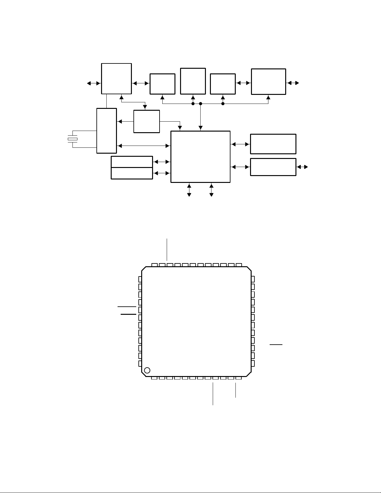
1.2 Functional Block Diagram
USB
6 MHz
USB Serial
SOF
OSC
PLL
ACG
Interface
Engine
8K ROM
6016 Byte RAM
UBM DMA
Suspend
/Resume
Logic
1520 Byte
SRAM
Port–3 Port–1
1.3 Terminal Assignments—Normal Mode
PFB PACKAGE (Normal Mode)
CDATI
CSYNC
(TOP VIEW)
DD
DV
CRESET
CSCHNE
8052 Core
P1.7
P1.6
P1.5
SS
DV
P1.4
P1.3
P1.2
CODEC
Interface
Global
Control/Status
Registers
2
I
C
Control
C–Port
I2C Bus
CSCLK
CDATO
MCLKO1
MCLKO2
RESET
VREN
SDA
SCL
AV
SS
XTALO
XTALI
PLLFILI
35 34 33 32 3136 30
37
38
39
40
41
42
43
44
45
46
47
48
23
1
DD
AV
PLLFILO
TAS1020A
5678
4
SS
DV
MCLKI
PUR
DP
DM
DD
DV
28 27 2629
9 10 11 12
TEST
EXTEN
MRESET
25
24
23
22
21
20
19
18
17
16
15
14
13
RSTO
P1.1
P1.0
NC
DV
DD
NC
P3.5
P3.4
P3.3
DV
SS
P3.2/XINT
P3.1
P3.0
1–3
Page 10
1.4 Terminal Assignments—External MCU Mode
CSCLK
CDATO
MCLKO1
MCLKO2
RESET
VREN
SDA
SCL
AV
SS
XTALO
XTALI
PLLFILI
PFB PACKAGE (External Mode)
(TOP VIEW)
DD
CDATI
CSYNC
35 34 33 32 3136 30
37
38
39
40
41
42
43
44
45
46
47
48
23
1
DD
AV
CRESET
4
MCLKI
MCUAD7
DV
CSCHNE
TAS1020A
5678
SS
DP
PUR
DV
PLLFILO
SS
MCUAD5
MCUAD6
DV
28 27 2629
9
DD
DM
DV
MRESET
MCUAD4
MCUAD3
10 11 12
TEST
EXTEN
MCUAD2
25
24
23
22
21
20
19
18
17
16
15
14
13
RSTO
MCUAD1
MCUAD0
MCURD
DV
DD
MCUWR
MCUINTO
MCUALE
MCUA10
DV
SS
XINT
MCUA9
MCUA8
1.5 Ordering Information
Texas Instruments
Audio Solutions
Peripheral Device
Package Type
TQFP
48 pins PFB
T PFB1020AAS
1–4
Page 11

1.6 Terminal Functions—Normal Mode
TERMINAL
NAME
AV
DD
AV
SS
CSCLK CMOS 37 I/O Codec port interface serial clock: CSCLK is the serial clock for the codec port interface used to clock
CSYNC CMOS 35 I/O Codec port interface frame sync: CSYNC is the frame synchronization signal for the codec port
CDATO CMOS 38 I/O Codec port interface serial data out
CDATI CMOS 36 I/O Codec port interface serial data in
CRESET CMOS 34 I/O Codec port interface reset output
CSCHNE CMOS 32 I/O Codec port interface secondary channel enable
DP CMOS 6 I/O USB differential pair data signal plus. DP is the positive signal of the bidirectional USB differential
DM CMOS 7 I/O USB differential pair data signal minus. DM is the negative signal of the bidirectional USB differential
DV
DD
DV
SS
EXTEN CMOS 11 I External MCU mode enable: Input used to enable the device for the external MCU mode
MCLKI CMOS 3 I Master clock input. An input that can be used as the master clock for the codec port interface or the
MCLKO1 CMOS 39 O Master clock output 1: The output of the ACG that can be used as the master clock for the codec port
MCLKO2 CMOS 40 O Master clock output 2: An output that can be used as the master clock for the codec port interface and
MRESET CMOS 9 I Master reset: An active low asynchronous reset for the device that resets all logic to the default state
NC 20,22 Not used
P1.[0:7] CMOS 23, 24,
P3.[0:6] CMOS 13, 14,
PLLFILI CMOS 48 I PLL loop filter input: Input to on-chip PLL from external filter components
PLLFILO CMOS 1 O PLL loop filter output: Output from on-chip PLL to external filter components
PUR CMOS 5 O USB data signal plus pullup resistor connect. PUR is used to connect the pullup resistor on the DP
RESET CMOS 41 O General-purpose active-low output which is memory mapped
RSTO CMOS 12 O Reset output: An output that is active while the master reset input or the USB reset is active
SCL CMOS 44 O I2C interface serial clock
SDA CMOS 43 I/O I2C interface serial data
TEST CMOS 10 I Test mode enable: Factory test mode
VREN CMOS 42 O General-purpose active-low output which is memory mapped
XINT CMOS 15 I External interrupt: An active low input used by external circuitry to interrupt the on-chip 8052 MCU
XTALI CMOS 47 I Crystal input: Input to the on-chip oscillator from an external 6-MHz crystal
XTALO CMOS 46 O Crystal Output: Output from the on-chip oscillator to an external 6-MHz crystal
PIN
TYPE
Power 2 3.3-V analog supply voltage
Power 45 Analog ground
Power 8, 21, 33 3.3-V digital supply voltage
Power 4, 16, 28 Digital ground
NO.
25, 26,
27, 29,
30, 31
15, 17,
18, 19
I/O DESCRIPTION
the CSYNC, CDATO, CDATI, CRESET,
interface.
pair used to connect the TAS1020A device to the universal serial bus.
pair used to connect the TAS1020A device to the universal serial bus.
source for MCLKO2.
interface and the codec.
the codec used in I2S modes for receive. This clock signal can also be used as a miscellaneous
clock.
I/O General-purpose I/O port [bits 0 through 1]: A bidirectional 8-bit I/O port with an internal 100 µA
active pullup
I/O General-purpose I/O port [bits 0 through 1]: A bidirectional I/O port with an internal 100 µA active
pullup
signal from a high-impedance state to 3.3 V . When the DP signal is connected to 3.3-V the host PC
detects the connection of the TAS1020A device to the universal serial bus.
AND CSCHNE signals.
1–5
Page 12

1.7 Terminal Functions—External MCU Mode
TERMINAL
NAME
AV
DD
AV
SS
CSCLK CMOS 37 I/O Codec port interface serial clock: CSCLK is the serial clock for the codec port interface used to
CSYNC CMOS 35 I/O Codec port interface frame sync: CSYNC is the frame synchronization signal for the codec port
CDATO CMOS 38 I/O Codec port interface serial data output
CDATI CMOS 36 I/O Codec port interface serial data input
CRESET CMOS 34 I/O Codec port interface reset output
CSCHNE CMOS 32 I/O Codec port interface secondary channel enable
DP CMOS 6 I/O USB differential pair data signal plus: DP is the positive signal of the bidirectional USB differential
DM CMOS 7 I/O USB differential pair data signal minus. DM is the negative signal of the bidirectional USB differen-
DV
DD
DV
SS
EXTEN CMOS 11 I External MCU mode enable: Input used to enable the device for the external MCU mode. This sig-
MCLKI CMOS 3 I Master clock input: An input that can be used as the master clock for the codec port interface or the
MCLKO1 CMOS 39 O Master clock output 1: The output of the ACG that can be used as the master clock for the codec
MCLKO2 CMOS 40 O Master clock output 2: An output that can be used as the master clock for the codec port interface
MRESET CMOS 9 I Master reset: An active low asynchronous reset for the device that resets all logic to the default
MCUAD
[0:7]
MCUA
[8:10]
MCUALE CMOS 18 I MCU address latch enable: Address latch enable for external MCU access to the TAS1020A exter-
MCUINTO CMOS 19 O MCU interrupt output: Interrupt output to be used for external MCU INTO input signal. All internal
MCUWR CMOS 20 I MCU write strobe: Write strobe for external MCU write access to the TAS1020A external data
MCURD CMOS 22 I MCU read strobe: Read strobe for external MCU read access to the TAS1020A external data
PLLFILI CMOS 48 I PLL loop filter input: Input to on-chip PLL from external filter components.
PLLFILO CMOS 1 O PLL loop filter output: Output to on-chip PLL from external filter components.
PUR CMOS 5 O USB data signal plus pullup resistor connect. PUR is used to connect the pullup resistor on the DP
RESET CMOS 41 O General-purpose active-low output which is memory mapped
RSTO CMOS 12 O Reset output: An output that is active while the master reset input or the USB reset is active.
SCL CMOS 44 O I2C interface serial clock
SDA CMOS 43 I/O I2C interface serial data input/output
TEST CMOS 10 I Test mode enable: Factory text mode
PIN
TYPE
Power 2 – 3.3-V Analog supply voltage
Power 45 – Analog ground
Power 8, 21, 33 – 3.3-V Digital supply voltage
Power 4, 16, 28 – Digital ground
CMOS 23, 24, 25,
CMOS 13, 14, 17 I/O MCU address bus: Multiplexed address bus bits[8:10] for external MCU access to the TAS1020A
NO.
26, 27, 29,
30, 31
I/O DESCRIPTION
clock the CSYNC, CDATO, CDATI, CRESET
interface.
pair used to connect the TAS1020A device to the universal serial bus.
tial pair used to connect the TAS1020A device to the universal serial bus.
nal uses a 3.3 V TTL/LVCMOS input buffer.
source for MCLKO2.
port interface and the codec.
and the codec. This clock signal can also be used as a miscellaneous clock.
state.
I/O MCU multiplexed address/data: Multiplexed address bits[0:7]/data bits[0:7] for external MCU ac-
cess to the TAS1020A external data memory space.
external data memory space.
nal data memory space.
TAS1020A interrupt sources are read together to generate this output signal.
memory space.
memory space.
signal to 3.3V from a high-impedance state. When the DP signal is connected in a 3.3-V state, the
host PC should detect the connection of the TAS1020A device to the universal serial bus.
AND CSCHNE signals.
1–6
Page 13
1.7 Terminal Functions—External MCU Mode (Continued)
GP
AIC
AC 97 v1.X
AC 97 v2.X
I2S
I2S
TERMINAL
NAME
VREN CMOS 42 O General-purpose active-low output which is memory mapped.
XINT CMOS 15 I External interrupt: An active low input used by external circuitry to interrupt the on-chip 8052 MCU.
XTALI CMOS 47 I Crystal input: Input to the on-chip oscillator from an external 6-MHz crystal.
XTALO CMOS 46 O Crystal output: Output from the on-chip oscillator to an external 6-MHz crystal.
PIN
TYPE
NO.
I/O DESCRIPTION
1.8 Device Operation Modes
The EXTEN and TEST pins define the mode that the TAS1020A is in after reset.
MODE EXTEN TEST
Normal mode – internal MCU 0 0
External MCU mode 1 0
Factory test 0 1
Factory test 1 1
1.9 Terminal Assignments for Codec Port Interface Modes
The codec port interface has five modes of operation that support AC97, I2S, and AIC codecs. There is also a
general-purpose mode that is not specific to a serial interface. The mode is programmed by writing to the mode select
field of the codec port interface configuration register 1 (CPTCNF1). The codec port interface terminals CSYNC,
CSCLK, CDATO, CDATI, CRESET
shown in the following table.
, and CSCHNE take on functionality appropriate to the mode programmed as
TERMINAL
NO. NAME
35 CSYNC CSYNC I/O FS O SYNC O SYNC O LRCK O LRCK1 O
37 CSCLK CSCLK I/O SCLK O BIT_CLK I BIT_CLK I SCLK O SCLK1 O
38 CDATO CDATO O DOUT O SD_OUT O SD_OUT O SDOUT1 O SDOUT1 O
36 CDATI CDATI I DIN I SD_IN I SD_IN1 I SDIN1 I SDIN2 I
34 CRESET CRESET O RESET O RESET O RESET O CRESET O SCLK2 O
32 CSCHNE NC O FC O NC O SD_IN2 I SDIN2 I LRCK2 O
NOTES: 1. Signal names and I/O direction are with respect to the TAS1020A device. The signal names used for the TAS1020A terminals for
the various codec port interface modes reflect the nomenclature used by the codec devices.
2. NC indicates no connection for the terminal in a particular mode. The TAS1020A device drives the signal as an output for these
cases.
3. The CSYNC and CSCLK signals can be programmed as either an input or an output in the general-purpose mode.
GP AIC AC ’97 v1.X AC ’97 v2.X
Mode 0
Mode 1
Mode 2
Mode 3
I2S I2S
Mode 4
Mode 5
1–7
Page 14

1–8
Page 15

2 Description
2.1 Architectural Overview
2.1.1 Oscillator and PLL
Using an external 6-MHz crystal, the TAS1020A derives the fundamental 48-MHz internal clock signal using an
on-chip oscillator and PLL. Using the PLL output, the other required clock signals are generated by the clock
generator and adaptive clock generator.
2.1.2 Clock Generator and Sequencer Logic
Utilizing the 48-MHz output from the PLL, the clock generator logic generates all internal clock signals, except for the
codec port interface master clock (MCLK) and serial clock (CSCLK) signals. The T AS1020A internal clocks include
the 48-MHz clock, a 24-MHz clock, and a 12-MHz clock. A 12 MHz USB clock is also generated. The USB clock is
the same as the internal 12-MHz clock when the T AS1020A is transmitting data, but is derived from the data when
the T AS1020A is receiving data. T o derive the USB clock when receiving USB data, the T AS1020A utilizes an internal
digital PLL (DPLL) driven from the 48-MHz clock.
The sequencer logic controls the access to the SRAM used for the USB endpoint configuration blocks and the USB
endpoint buffer space. The SRAM can be accessed by the MCU, the USB buffer manager (UBM), or the DMA
channels. The sequencer controls the access to the memory using a round-robin fixed priority arbitration scheme.
This means that the sequencer logic generates grant signals for the MCU, UBM, and DMA channels at a
predetermined fixed frequency.
2.1.3 Adaptive Clock Generator (ACG)
The adaptive clock generator is used to generate a master clock output signal (MCLKO) to be used by the codec port
interface and the codec device. To synchronize data sent to or received from the codec to the USB frame rate, the
MCLKO signal generated by the adaptive clock generator must be used. The synchronization of the MCLKO signal
to the USB frame rate is achieved by the ACG, which, in turn, is controlled by a soft PLL, implemented in the MCU.
One of the tasks performed by the ACG is to maintain count of the number of MCLKO clocks between USB Start of
Frame (SOF) events. This count is monitored by the soft PLL in the MCU. Based on this count, the soft PLL outputs
corrections to the ACG to adjust MCLKO to obtain the correct number of MCLKO clocks between USB SOF events.
MCLKI, the master clock input, can also be selected to source the clocks used by the codec port interface. When
MCLKI is selected, it is used to derive the TAS1020A-sourced versions of the clocks CSCLK and CSYNC. In this
scenario, the codec device would also use the same master clock signal (MCLKI).
2.1.4 USB Transceiver
The TAS1020A provides an integrated transceiver for the USB port. The transceiver includes a differential output
driver, a dif ferential input receiver , and two single ended input buf fers. The transceiver connects to the USB DP and
DM signal terminals.
2.1.5 USB Serial Interface Engine (SIE)
The serial interface engine logic manages the USB packet protocol for packets being received and transmitted by
the T AS1020A. For packets being received, the SIE decodes the packet identifier field (PID) to determine the type
of packet being received and to ensure the PID is valid. The SIE then calculates the cycle redundancy check (CRC)
of the received token and data packets and compares the value to the CRC contained in the packet to verify that the
packet was not corrupted during transmission. For transmitted token and data packets, the SIE generates the CRC
that is transmitted with the packet. The SIE also generates the synchronization field (SYNC) and the correct PID for
all transmitted packets. Another major function of the SIE is the serial-to-parallel conversion of received data packets
and the parallel-to-serial conversion of transmitted data packets.
2–1
Page 16

2.1.6 USB Buffer Manager (UBM)
The USB buffer manager provides the control logic that interfaces the SIE to the USB endpoint buffers. One of the
major functions of the UBM is to decode the USB function address to determine if the host PC is addressing the
T AS1020A device USB peripheral function. In addition, the endpoint address field and direction signal are decoded
to determine which particular USB endpoint is being addressed. Based on the direction of the USB transaction and
the endpoint number, the UBM will either write or read the data packet to or from the appropriate USB endpoint data
buffer.
2.1.7 USB Frame Timer
The USB frame timer logic receives the start of frame (SOF) packet from the host PC each USB frame. Each frame,
the logic stores the 1 1-bit frame number value from the SOF packet in a register and asserts the internal SOF signal.
The frame number register can be read by the MCU and the value can be used as a time stamp. For USB frames
in which the SOF packet is corrupted or not received, the frame timer logic will generate a pseudo start of frame
(PSOF) signal and increment the frame number register.
2.1.8 USB Suspend and Resume Logic
The USB suspend and resume logic detects suspend and resume conditions on the USB. This logic also provides
the internal signals used to control the TAS1020A device when these conditions occur. The capability to resume
operation from a suspend condition with a locally generated remote wake-up event is also provided.
2.1.9 MCU Core
The T AS1020A uses an 8-bit microcontroller core that is based on the industry standard 8052. The MCU is software
compatible with the 8052, 8032, 80C52, 80C53, and 87C52 MCUs. The 8052 MCU is the processing core of the
T AS1020A and handles all USB control, interrupt and bulk endpoint transfers. Bulk out end-point transfers can also
be handled by one of the two DMA channels.
2.1.10 MCU Memory
In accordance with the industry standard 8052, the TAS1020A MCU memory is organized into program memory,
external data memory and internal data memory . A boot ROM program is used to download the application code to
a 6K byte RAM that is mapped to the program memory space. The external data memory includes the USB endpoint
configuration blocks, USB data buffers, and memory mapped registers. The total external data memory space
available is 1.5K bytes. A total of 256 bytes are provided for the internal data memory.
2.1.11 USB Endpoint Configuration Blocks and Buffer Space
The USB endpoint configuration blocks are used by the MCU to configure and operate the required USB endpoints
for a particular application. In addition to the control end-point, the T AS1020A supports a total of seven IN endpoints
and seven OUT endpoints. A set of six bytes is provided for each endpoint to specify the endpoint type, buffer address,
buffer size, and data packet byte count.
The USB endpoint buffer configuration blocks and buffer space provided totals 1440 bytes. The buffer space to be
used by a particular endpoint is fully configurable by the MCU for a particular application. Therefore, the MCU can
configure each buffer based on the total number of endpoints to be used, the maximum packet size to be used for
each endpoint, and the selection of single or double buffering.
2.1.12 DMA Controller
Two DMA channels are provided to support the streaming of data for USB isochronous IN endpoints, isochronous
OUT endpoints, and bulk OUT endpoints. Each DMA channel can support one USB isochronous IN endpoint, or one
isochronous OUT endpoint, or one bulk OUT endpoint. The DMA channels are used to stream data between the USB
2–2
Page 17

endpoint data buffers and the codec port interface. The USB endpoint number and direction can be programmed for
each DMA channel. Also, the codec port interface time slots to be serviced by each DMA channel can be
programmed.
2.1.13 Codec Port Interface
The T AS1020A provides a configurable full duplex bidirectional serial interface that can be used to connect to a codec
or other external device types for streaming USB isochronous data. The interface can be configured to support
several different industry standard protocols, including AC ’97 1.X, AC ’97 2.X, AIC, and I
a general-purpose mode to support other protocols.
2
S. The T AS1020A also has
2.1.14 I2C Interface
The I2C interface logic provides a two-wire serial interface that the 8052 MCU can use to access other ICs. The
TAS1020A is an I
interface can be programmed to operate at either 100 kbps or 400 kbps. In addition, the protocol supports 8-bit or
16-bit addressing for accessing the I
means slaves can assert wait state on the I
2
C master device only and supports single byte or multiple byte read and write operations. The
2
C slave device memory locations. The T AS1020A supports I2C wait states. This
2
C bus by pulling the SCL line low.
2.1.15 General-Purpose IO Ports (GPIO)
The T AS1020A provides two general-purpose IO ports that are controlled by the internal 8052 MCU. The two ports
are port 1 and port 3. Port 1 provides true GPIO capability. Each bit of port 1 can be independently used as either
an input or output, and consists of an output buffer , an input buffer, and a pullup resistor. Some of the bits of port 3
also provide true GPIO capability , but, in addition, some of the bits of port 3 also provide alternate input and output
uses. An example of this is P3.2, which is used as the external interrupt (XINT
description of the alternate uses of some of the port 3 bits is presented in Section 2.2.11.
The pullup resistors for port 1 and port 3 can be disabled by bits P1PUDIS and P3PUDIS respectively in the on-chip
register GLOBCTL. In addition, any port 3 pin can be used to wake up the host PC from a low-power suspend mode.
) input to the TAS1020A. A detailed
2.1.16 Interrupt Logic
The interrupt logic monitors the various conditions that can cause an interrupt and asserts the interrupt 0 (INTO) input
on the 8052 MCU core accordingly . All of the TAS1020A internal interrupt sources and the external interrupt (XINT
input are ORed together to generate the INT0 signal. An interrupt vector register is used by the MCU to identify the
interrupt source.
2.1.17 Reset Logic
)
An external master reset (MRESET) input signal that is asynchronous to the internal clocks can be used to reset the
T AS1020A logic. In addition to this master reset, the T AS1020A logic can also be reset by a USB reset from the host
PC if bit FRSTE in the on-chip register USBCTL is set to 1. The T AS1020A also provides a reset output (RSTO
that can be used by external devices. This signal is asserted when either a master reset occurs or when a USB reset
occurs and FRSTE is set to 1.
) signal
2.2 Device Operation
The operation of the T AS1020A is explained in the following sections. For additional information on USB, refer to the
Universal Serial Bus Specification, Version 1.1.
2–3
Page 18

2.2.1 Clock Generation
The T AS1020A requires an external 6-MHz crystal with load capacitors and PLL loop filter components to derive all
the clocks needed for both USB and codec operation. Figure 4–1 shows the connection of these components to the
T AS1020A. Figure 4–1 also shows a ground shield residing on the top layer of the PCB and underneath the crystal
and its load capacitors and the PLL components. The PLL is an analog PLL, and noise pickup in these components
can translate to phase jitter at the output of the PLL, which in turn can translate to distortion at the codec. A ground
shield is recommended to attenuate the digital noise components on the board as seen at the PLL.
The A V
the digital noise residing on a board, A V
and A VDD pins on the T AS1020A are used exclusively to power the analog PLL. T o maintain isolation from
SS
should be a separate ground plane that connects to the primary ground
SS
plane (DGND) at a single point via a ferrite bead. The ferrite bead should exhibit around 9 Ω of impedance at 100 MHz.
AV
should also be distinct from DVDD. A recommended architecture is to generate DVDD and A VDD from the same
DD
regulator line, with each derived from a RC filter in series with the regulator output. It is finally recommended that the
ground shield for the crystal and its load capacitors and the PLL loop filter components be connected to A V
SS
at a
single point via a ferrite bead of the same type as above.
Using the low frequency 6-MHz crystal and generating the required higher frequency clocks internally in the
TAS1020A is a major advantage with regard to EMI.
2.2.2 Boot Process
The T AS1020A can boot from EEPROM or execute a host boot. Host boot will be used in the following circumstances:
• No EEPROM is present.
• An EEPROM is present, but does not contain a valid header.
• An EEPROM is present, but is a device EEPROM (contains header information only).
2.2.2.1 EEPROM Boot Process
If the target device has an application EEPROM (an EEPROM that contains both header and application data), and
if the header portion of the EEPROM content is valid, the EEPROM application code is downloaded to on-chip RAM.
During the download process, the RAM is mapped to data space, and the boot code that orchestrates the download
is part of the on-chip firmware housed in on-chip ROM. Also, while the application code is being downloaded, the
TAS1020A remains disconnected from the USB bus.
When the download is complete, the firmware sets the ROM disable bit SDW. The setting of this bit maps the RAM
from data space to program space, starting address 0x0000. Having set bit SDW, the firmware then branches to
address 0x0000, which is the reset entry point for the application code. The application code is now running.
The application code then switches on the PUR output. The PUR output pin is connected, through a resistor, to the
positive (DP) line of the differential USB bus. Switching PUR on informs the host that a full speed (12 Mb/s) device
is present on the bus. In the enumeration procedure that follows, the application code reports its run-time device
descriptor set. Following enumeration, the device is actively running its application.
2.2.2.2 Host Boot Process
The DFU code in the TAS1020A fully adheres to the USB Device Class Specification for DFU 1.0. In addition, the
T AS1020A utilizes the communication protocols from the DFU specification to implement a host boot capability for
those applications that do not have an EEPROM resource. In such cases, the TAS1020A, at power-up, reports its
DFU mode descriptor set rather than its run-time descriptor set and directly enters what the DFU specification terms
the DFU Program Mode. The host processor must be cognizant of the fact that the device under enumeration does
not have an EEPROM resource with valid code, and is already in the DFU mode awaiting a download per the DFU
protocol. All of this capability is provided by the ROM-based code (firmware) that resides on the TAS1020A.
Specifically, the host boot process addresses three cases—an EPROM is not present, an EEPROM is present but
the data in the EEPROM is invalid, or an EEPROM is present but the EEPROM is a device EEPROM (contains only
2–4
Page 19

header data). In all three of these cases, the T AS1020A firmware comes up in the DFU Program Mode. A host boot
ensues, but the final destination of the download depends on the status of the onboard EEPROM.
• If the firmware determines that no EEPROM is present (by noting, when addressing the EEPROM, the
absence of an acknowledge from the EEPROM), a Vendor ID of 0xFFFF and a Product ID of 0xFFFE is
reported during enumeration. The download that follows enumeration is written to the on-chip RAM. The
download from the host must include a header (see Section 2.2.2.3.1), and the header overwrite bit in the
header downloaded must be set to 0. (The header overwrite bit is used to instruct the T AS1020A firmware
as to whether or not the header portion of the download is to be written into the EEPROM. Since, in this case,
no EEPROM is present, this header overwrite bit must be set to 0). It is noted that the host must have prior
knowledge that the target will initialize in the DFU program mode and will require a download of application
code (and header) to RAM.
• If the firmware determines that an EEPROM is present (acknowledges are received from the EEPROM),
but that the header data in the EEPROM is invalid, a Vendor ID of 0xFFFF and a Product ID of 0xFFFE is
reported during enumeration. The download that follows enumeration is written to EEPROM. Since the
EEPROM data was invalid, the host has to set the header overwrite bit in the header portion of the download
to a 1 to ensure that the header is written to the EEPROM. It is noted that the host must have prior knowledge
that the target does have an EEPROM, but that the data in the EEPROM is invalid. This could be a situation
such as the initial download of the application on a production line.
• If the firmware determines that an EEPROM is present, that the header data in the EEPROM is valid, but
that the header data in the EEPROM indicates that the EEPROM is a device EEPROM, the Vendor ID and
Product ID settings in the EEPROM-resident header is reported during enumeration. In addition, the strings
in the header, if applicable, are reported. The EEPROM download that follows enumeration will be written
to the on-chip RAM facility . In addition to downloading the application code to RAM, an option also exists
to download the header portion of the download image to the EEPROM. If the host does not wish to
overwrite the valid header data in the EEPROM, it must set the header overwrite bit in its download header
to a 0. It is noted that the host must have knowledge that the target contains an EEPROM, and that the
EEPROM is a device EEPROM.
2.2.2.3 EEPROM Data Organization
Two types of data can be stored in the EEPROM—header data, which contains USB device information, and
application code. The presence of header data in the EEPROM is mandatory , but the presence of application code
is optional.
2–5
Page 20

2.2.2.3.1 EEPROM Header
Table 2–1 shows the format and information contained it the header data. As seen from Table 2–1, the header data
begins at address 0x0000 in the EEPROM and precedes the application code.
Table 2–1. EEPROM Header
OFFSET TYPE SIZE VALUE
0 headerChksum 1 Header check sum—derived by adding the header data, excluding the header checksum, in bytes, and
1 HeaderSize 1 Size, in units of bytes, of the header including strings if applied
2 Signature 2 Signature: 0x1234
4 VendorID 2 USB Vendor ID
6 ProductID 2 USB Product ID
8 ProductVersion 1 Product version
9 FirmwareVersion 1 Firmware version
10 UsbAttributes 1 USB attributes:
11 MaxPower 1 Maximum power the device needs in units of 2 mA.
12 Attributes 1 Device attributes:
13 WPageSize 1 Maximum I2C write page size, in units of bytes
14 DataType 1 This value defines if the device is an application EEPROM or a device EEPROM.
15 RpageSize 1 Maximum I2C read page size, in units of bytes. If the value is zero, the whole payLoadSize is read in one
16 payLoadSize 2 Size, in units of bytes, of the application, if using EEPROM as an application EEPROM, otherwise the
xxxx Language string 4 Language string in standard USB string format if applied. If this attribute is applied, the two attributes
xxxx Manufacture string ... Manufacture string in standard USB string format if applied.
xxxx Product string ... Product string in standard USB string format if applied.
xxxx Application Code ... Application code if applied
retaining the lower byte of the sum as the checksum.
Bit 0: If set to 1, the header includes all three strings: language, manufacture, and product strings, if set
to 0, the header does not include any string. The strings, if present, must conform to the USB
string format per USB spec 1.0 or later.
Bit 1 : Not used.
Bit 2: If set to 1, the device can be self powered, if set to 0, cannot be self powered.
Bit 3: If set to 1, the device can be bus powered, if set to 0, cannot be bus powered.
Bit 4 ... 7: Reserved
Bit 0: If set to 1, the CPU clock is 24 MHz, if set to 0, the CPU clock is 12 MHz.
Bit 1: If set to 1, the download version of the header will be written into the EEPROM (download target
has to be EEPROM). If the header is not to be overwritten, or if the target is RAM, this bit must be
cleared to 0.
Bit 2: Not used.
Bit 3: If set to 1, the EEPROM can support a 400 kHz I2C bus, if set to 0, the EEPROM cannot support
a 400 MHz I2C bus.
Bit 4 ... 7: Reserved
0x01: Application EEPROM—contains header and application code.
0x02: Device EEPROM—contains only header.
All other values are invalid.
I2C read setup.
value is 0.
that follow must also be applied. If this attribute is not applied, the following two attributes cannot be
applied.
The header checksum is used by the firmware to detect the presence of a valid header in the EEPROM. The header
size field supports future updates of the header.
2.2.2.3.2 Application Code
Application code is stored as a binary image in the EEPROM following the header information. The binary image must
always be mapped to MCU program space starting at address 0x0000, and must be stored in the EEPROM as a
continuous linear block of data.
2–6
Page 21

2.2.2.4 I2C Serial EEPROM
The TAS1020A accesses the EEPROM via an I2C serial bus. Thus the EEPROM must be an I2C serial EEPROM.
The ROM boot loader assumes the EEPROM device uses the full 7-bit I
of the address (control code) set to 1010 and the three least significant bits (chip select bits) set to 000.
2
C device address with the upper four bits
2.2.2.5 DFU Upgrade Process
DFU compliance provides a host the capability of upgrading application code currently residing in a target’s onboard
EEPROM memory. The DFU upgrade process provided by the TAS1020A fully conforms to the requirements
specified in USB Device Class Specification For DFU 1.0.
The download must consist of both header and application code. The destination of the download must be defined
by the on-chip application code (as opposed to the application code being downloaded). Under normal
circumstances, the download destination would be EEPROM, but it is possible for the application code to specify
on-chip RAM as the download destination.
If the download destination is to be EEPROM, bit 1 of the Attribute field in the header data being downloaded
determines whether or not the header data in the download image is to be written to the EEPROM. A bit value of 1
results in the header in the EEPROM being overwritten by the header content in the download image. It is important
to note that if the application code targets RAM as the download destination, bit 1 in the Attribute field of the download
image must be 0.
2.2.2.6 Download Error Recovery
Safeguards are incorporated on the T AS1020A ROM to allow recovery from a host download that does not complete
due to a loss of power. Before downloading the application code, the TAS1020A saves the value of the Data Type
field in the EEPROM header and modify the Data Type field to indicate that a download is in progress. After successful
completion of the download, the TAS1020A restores the saved value in the Data Type field. If the download is
terminated prior to successful completion, the Data Type field still indicates that a download is in progress. In the case
of an unsuccessful download the T AS1020A reboots as a DFU device in DFU Program mode and uses the Vendor
and Product ID from the EEPROM header as the vendor and product ID in its USB device descriptor.
The download process consists of the following task flow.
• Header portion of download is written to EEPROM, if applicable.
• Header Data Type is retrieved and stored in RAM.
• Head Data Type is overwritten with a value indicating that a download is in progress.
• Application portion of download is written to EEPROM (or to RAM).
• Header Data Type is overwritten with the previously recorded legal value.
If the download should terminate during the downloading of the header to EEPROM, the header checksum results
in the EEPROM being declared invalid on the next boot of the T AS1020A. If the download should terminate during
the downloading of the application code, the Data Type field indicates that a download was in progress and the
TAS1020A enters the DFU program mode on the next boot.
If the T AS1020A remains powered when a premature termination of a download occurs, the TAS1020A remains in
the DFU program mode. In this case, the host can again attempt a download; the TAS1020A does not have to be
rebooted.
2–7
Page 22

2.2.2.7 ROM Support Functions
In order to conserve RAM memory resources on the T AS1020A, several USB-specific routines have been included
in the firmware resident in the on-chip ROM. The inclusion of these routines frees the application code from having
to implement USB-specific code.
The tasks provided by the ROM code include:
• A USB engine for handling USB control endpoint data transactions and states
• USB protocol handlers to support USB Chapter 9
• USB protocol handlers to support USB HID Class
• USB protocol handlers to support USB DFU Class
• USB protocol handlers to support the common features of USB Audio Class commands
• Feature Unit:
– Set/get volume control
– Set/get mute control
– Set/get bass control
– Set/get treble control
• Mixer unit: set/get input/output gain control
• End point: set/get the audio streaming endpoint sampling frequency
• For unsupported case, the ROM code passes the requests to the application code for processing.
2.2.3 USB Enumeration
USB enumeration is accomplished by interaction between the host PC and the T AS1020A. As described in Section
2.2.2, the TAS1020A can identify itself as an application device by reporting its application Vendor ID and Product
ID, or it can identify itself as a DFU device by reporting a Vendor ID of 0xFFFF and a Product ID of 0xFFFE. If the
TAS1020A fails to detect the presence of an EEPROM, or if an EEPROM is present but does not contain a valid
header, the Vendor ID of 0xFFFF and Product ID of 0xFFFE are reported. If an EEPROM is present, but contains
only valid header data, the Vendor ID and Product ID settings in the EEPROM header are reported, but the T AS1020A
firmware comes up as a DFU device in the DFU program mode. If an EEPROM is present, and contains both a valid
header and application code, the TAS1020A comes up as an application specific device.
For all cases where the TAS1020A comes up in the DFU program mode, once application code has been
downloaded, the TAS1020A is reset by a host-issued USB reset. After this reset, the TAS1020A comes up as an
application device. When the T AS1020A comes up as an application device, the ROM-resident boot loader retrieves
the application code from the EEPROM, if the EEPROM is not a device EEPROM, and then runs the application code.
It is the application code that connects the TAS1020A to the USB. During the enumeration that follows connection
to the USB, the application code identifies the device as an application specific device and the host loads the
appropriate host driver(s).
The boot loader and application code both use the CONT , SDW and FRSTE bits to control the enumeration process.
• The function connect (CONT) bit is set to a 1 by the MCU to connect the T AS1020A device to the USB. When
this bit is set to a 1, the USB DP line pullup resistor (PUR) output signal is enabled. Enabling PUR connects
the pullup on the PCB to the T AS1020A 3.3-V digital supply voltage. (When the T AS1020A powers up, this
bit is cleared to a 0 and the PUR output is in the high-impedance state.) This bit is not affected by subsequent
USB resets.
• The shadow the boot ROM (SDW) bit is set to 1 by the MCU to switch the MCU memory configuration from
boot loader mode to normal operating mode. Once set to 1, this bit is not affected by subsequent USB resets.
• The function reset enable (FRSTE) bit is set to a 1 by the MCU to enable the USB reset to reset all internal
logic including the MCU. However, the shadow the ROM (SDW) and the USB function connect (CONT) bits
are not reset. In addition, when the FRSTE bit is set, the reset output (RSTO
device is active whenever a USB reset occurs. This bit, once set, is not affected by subsequent USB resets.
) signal from the TAS1020A
2–8
Page 23

2.2.4 TAS1020A USB Reset Logic
There are two mechanisms provided by the T AS1020A—an external reset MRESET and a USB reset. The reset logic
used in the TAS1020A is presented in Figure 2–2.
MRESET is a global reset that results in all the TAS1020A logic and the 8052 MCU core being reset. This input to
the TAS1020A is typically used to implement a power-on reset at the application of power, but it can also be used
with reset pushbutton switches and external circuits to implement global resets at any time. MRESET
asynchronous reset that must be active for a minimum time period of one microsecond.
The T AS1020A can also detect a USB reset condition. When this reset occurs, the TAS1020A responds by setting
the function reset (RSTR) bit in the USB status register (USBSTA). However, the extent to which the internal logic
is reset depends on the setting of the function reset enable bit (FRSTE) in the USB control register (USBCTL).
If the MCU has set FRSTE to 1, incoming USB resets are treated as global resets, with all T AS1020A logic and the
8052 MCU core being reset. However, the shadow the ROM (SDW) and the USB function connect (CONT) bits are
not reset. Also, if the USB reset results in a global reset being issued, an interrupt to the 8052 MCU is not generated.
But if the MCU has cleared FRSTE, incoming USB resets is treated as interrupts to the MCU (via INT0
corresponding function reset bit RSTR in the USB interrupt mask register USBMSK has been set by the MCU. If
neither FRSTE or RSTR has been set by the MCU, USB resets have no effect on the T AS1020A, other than resetting
the USB serial interface engine (SIE) and the USB buffer manager (UBM) in the TAS1020A.
Regardless of the status of FRSTE and bit RSTR in the USB interrupt mask register USBMSK, the function reset bit
RSTR in the USB status register USBST A is always set whenever a USB reset condition is detected. If the USB reset
results in the generation of a global reset, the global reset clears the function reset bit RSTR in USBST A. If, instead,
the USB reset results in an interrupt being generated, RSTR in register USBST A is cleared when the MCU writes to
the interrupt vector register VECINT while in the USB reset interrupt service routine (VECINT = 0x17).
is an
) if the
The TAS1020A has two reset outputs—RSTO
every time a USB reset occurs and bit FRSTE in the USB control register USBCTL is set. CRESET
as a codec reset. Although labeled a reset line, it has no direct relationship to MRESET
and CRESET. RSTO is activated every time MRESET is active, and
is typically used
or detected USB resets.
Instead, it is activated and deactivated when the on-chip 8052 MCU core writes a 0 and a 1, respectively , to the CRST
bit in the codec port interface control and status register CPTCTL.
2–9
Page 24

2.2.5 USB Suspend and Resume Modes
The TAS1020A can recognize a suspend state. Figure 2–2 shows the logical implementation of the suspend and
resume modes in the T AS1020A. The T AS1020A enters a suspend mode if a constant idle state (j state) is observed
on the USB bus for a period of 5 ms. USB compliance also requires that a device enter a suspend state, drawing only
suspend current from the bus, after no more than 10 ms of bus inactivity , The TAS1020A supports this requirement
by creating a suspend interrupt to the on-chip MCU after a suspend condition has been present for 5 ms. Upon
receiving this interrupt, the MCU firmware can then take the steps necessary to assure that the device enters a
suspend state within the next 5 ms.
There are two ways for the T AS1020A device to exit the suspend mode: 1) detection of USB resume signaling and
2) proactively performing a local remote wake-up event.
2.2.5.1 USB Suspend Mode
When a suspend condition is detected on the USB, the suspend/resume logic sets the function suspend request bit
(SUSR) in the USB status register, resulting in the generation of the function suspend request interrupt SUSR. To
enter the low-power suspend state and disable all T AS1020A device clocks, the MCU firmware, upon receiving the
SUSR interrupt, must set the idle mode bit (IDL), which is bit 0 in the MCU power control (PCON) register. Setting
the IDL bit results in the T AS1020A suspending all internal clocks, including the clocks to the MCU. The MCU thus
suspends instruction execution while in the idle mode.
The MCU must not set the IDL bit while in the SUSR interrupt service routine (ISR), or while in any other ISR. As
described in Section 2.2.5.3, it is intended that the receipt of an INT0
state. But if the MCU has suspended instruction execution while in an ISR, subsequent INT0
as the MCU is still servicing an interrupt. For this reason then, it is necessary that IDL not be set while processing
an ISR. (As described in Section 2.2.5.3, an external wake-up event will resume clocks within the TAS1020A. But
even if the clocks to the MCU resume, if the MCU does not recognize INT0
core itself remains in the suspend state).
interrupt at the MCU result in exiting the suspend
activity is not recognized,
, the IDL bit remains set and thus the MCU
The SUSR bit is cleared while in the SUSR ISR by writing to the interrupt vector register VECINT . While servicing the
SUSR ISR, the VECINT output is 0x16 – the USB function suspend interrupt vector. As shown in Figure 2–2, the
occurrence of a write to VECINT, while the USB function suspend interrupt vector is being output, results in clearing
bit SUSR of the USB status register. (The data written to VECINT is of no consequence; the clearing action takes place
upon decoding the write transaction to VECINT).
2.2.5.2 USB Resume Mode
When the TAS1020A is in a suspend state, any non-idle signaling on the USB is detected by the suspend/resume
logic and device operation resumes. When the resume signal is detected, the T AS1020A clocks are enabled and the
function resume request bit (RESR) is set, resulting in the generation of the function resume request interrupt. The
function resume request interrupt to the MCU automatically clears the idle mode bit IDL in the PCON register, and
as a result the MCU exits the suspend state and becomes fully functional, with all internal clocks active. After the RETI
from the ISR, the next instruction to be executed is the one following the instruction that set the IDL bit. The RESR
bit is cleared while in the RESR ISR by writing to the interrupt vector register VECINT.
2.2.5.3 USB Remote Wake-Up Mode
The TAS1020A device has the capability to remotely wake up the USB by generating resume signaling upstream,
providing the host has granted permission to generate remote wake-ups via a SET_FEATURE
DEVICE_REMOTE_W AKEUP control transaction. If remote wakeup capability has been granted, the MCU firmware,
upon awakening from a suspend state, has to activate the remote wake-up request bit RWUP in the USB control
register USBCTL. Activation of RWUP consists of the MCU firmware writing a 1 followed by a 0 to RWUP. This action
creates a pulse, which results in the T AS1020A generating resume signaling upstream by driving a k state (non-idle)
onto the USB bus. The USB specification requires that remote wake-up resume signaling not be generated until the
2–10
Page 25

suspend state has been active for at least 5 ms. In addition, the specification requires that the remote wake-up resume
signaling be generated for at least 1ms but for no more than 15 ms. The 5 ms requirement is met by not entering the
suspend mode until an idle state, or j state, is detected, uninterrupted, for 5 ms. The RWUP pulse results in driving
a k state onto the USB bus for 1 to 2 ms, and thus the 15 ms requirement is also met. Moreover, if an application wishes
to extend the duration of the k state on the USB bus, it need only extend the pulse width of RWUP. The resulting
duration of the resume signaling is the duration of the RWUP pulse plus 1 to 2 ms.
The condition that activates a remote wake-up is a transition from 1 to 0 on one of the P3 port bits whose
corresponding mask bit has been set to zero. (When in the suspend mode, the XINT
input is treated as port bit P3.2).
As seen in Figure 2–2, the P3 mask register bits are gated with the P3 port input lines from the I/O port cells. The
gated P3 port bits are then all ORed together and the output is ANDed with the suspend signal. The output of this
logic drives the clock input of a flip-flop, and when the output of this logic transitions from 0 to 1, the flip-flop is set
to 1. The setting of this flip-flop to 1 results in the TAS1020A exiting the suspend state and resuming all clocks,
including those to the MCU core. The output of this flip-flop is also gated with bit XINTEN in the global control register
GLOBCTL, and the output of this gate drives the INT0
an INT0
interrupt to the MCU only if bit XINTEN has been set. Therefore, before entering a suspend state, the firmware
interrupt logic. This means that a remote wake-up generates
must set XINTEN if remote wake-up capability is to be enabled.
The wake-up interrupt is seen by the firmware as an XINT
an output value of 0x1F. If the XINT
pin is to be used as an event marker during normal operation, and if one of the
interrupt; that is, the interrupt vector register VECINT has
P3 port bits is to be used for a wake-up interrupt, the firmware must be able to distinguish between a wake-up interrupt
and a normal XINT
register. If this bit is set, the interrupt event is a wake-up interrupt; otherwise, the interrupt is a normal XINT
If an XINT
event should occur during a suspend mode, the event is ignored if the mask bit for P3.2 is set. (During a
suspend mode the TAS1020A clocks are disabled, and thus an incoming XINT
through the synchronization logic and activate the MCU INT0
interrupt. One technique would be to examine the state of the IDL bit in the MCU power control
interrupt.
interrupt event does not propagate
input).
2.2.6 Adaptive Clock Generator (ACG)
The adaptive clock generator is used to generate two programmable master clock output signals (MCLKO and
MCLKO2) that can be used by the codec port interface and the codec device. Two separate and programmable
frequency synthesizers provide the two master clocks. This allows the TAS1020A to support different record and
playback rates for those devices that require separate master clocks to implement different rates. For isochronous
transactions, the ACG can also support USB asynchronous, synchronous, and adaptive modes of operation. The
ACG keeps count of the number of master clock events between USB SOF time marks, and the DCNTX/Y field of
the endpoint register IEPDCNTX/Y keeps track of the number of samples received between USB SOF time marks.
Synchronous isochronous operation can be accomplished by adjusting one of the two frequency synthesizers until
the correct number of master clock events is obtained between USB SOF time marks. Similarly, monitoring the
number of samples received between USB SOF events can accommodate adaptive isochronous operation. Here the
frequency synthesizer is adjusted to obtain the proper codec output rate for the number of samples received. The
TAS1020A can also accommodate asynchronous isochronous operation, and the input MCLKI is provided for this
case. For asynchronous isochronous operation, the external clock pin MCLKI is used to derive the data and sync
signal to the codec. However, the external clock that provides the input to pin MCLKI, instead of the master clock
output (MCLKO or MCLKO2) from the ACG, must also source the codec’s MCLK.
A block diagram of the adaptive clock generator is shown in Figure 2–1. Each frequency synthesizer circuit generates
a programmable clock with a frequency range of 12–25 MHz, and each frequency synthesizer output feeds a
divide-by-M-circuit, which can be programmed to divide by 1 to 16. As a result, the frequency range of each master
clock is 750 kHz to 25 MHz. Also, the duty cycle of each master clock is 50% for all programmable frequencies.
As indicated in Figure 2–1, multiplexers precede the master clocks MCLKO and MCLKO2. These multiplexers
provide the option of using the output of either frequency synthesizer (after division by the divide-by-M circuit) or the
MCLKI input (after division by the divide-by-I circuit) to source each master clock. Each master clock is also assigned
its own divide circuit to generate its associated CSCLK. The C-port serial clock (CSCLK) is derived by setting the
divide by B value in codec port interface configuration register CPTNCF4 [2:0] and the C-port serial clock2 (CSCLK2)
is derived by setting the divide by B2 value in codec port receive interface configuration register 4 CPTRXCNF4 [2:0].
2–11
Page 26
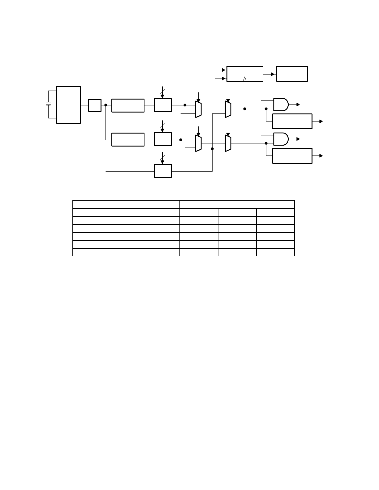
In addition, although not shown in Figure 2–1, each master clock is assigned its own CSYNC generator, with the
length and polarity of each CSYNC separately programmable.
6 MHz
Oscillator
PLL
MCLKI
Frequency
Synthesizer
Frequency
Synthesizer
ACG1DCTL[7:4]
Divide
1
by M1
ACG2DCTL[7:4]
Divide
2
by M2
ACG1DCTL[2:0]
Divide
by I
SOF
PSOF
4
4
3
ACGCTL[4]
ACGCTL[1]
16-Bit Counter
ACGCTL[3]
ACGCTL[6]
ACGCTL[0]
ACGCTL[7]
Figure 2–1. Adaptive Clock Generator
The ACG is controlled by the following registers. Refer to section A.5.3 for details.
FUNCTIONAL REGISTER ACTUAL BYTE-WIDE REGISTERS
24-bit frequency register #1 ACG1FRQ2 ACG1FRQ1 ACG1FRQ0
16-bit capture register ACGCAPH ACGCAPL
8-bit synthesizer 1 divider control register ACG1DCTL
8-bit ACG control register ACGCTL
24-bit frequency register #2 ACG2FRQ2 ACG2FRQ1 ACG2FRQ0
8-bit synthesizer 2 divider control register ACG2DCTL
ACGCAPH
ACGCAPL
MCLK0
Divide by B
CPTCNF4 [2:0]
MCLK02
Divide by B2
CPTRXCNF4 [2:0]
CSCLK
CSCLK2
The main functional modules of the ACG are described in the following sections.
2.2.6.1 Programmable Frequency Synthesizer
The 24-bit ACG frequency register value is used to program the frequency synthesizer, and the value of the frequency
register can be updated by the MCU while the ACG is running. The high resolution of each frequency value
programmed allows the firmware to adjust the frequency value by +LSB or more to lock onto the USB start-of-frame
(SOF) signal and achieve a synchronous mode of operation, a necessity for streaming audio applications. The 24-bit
frequency register value is updated and used by the frequency synthesizer only when MCU writes to the ACGFRQ0
register. The proper way to update a frequency value then is to write the least significant byte (ACGFRQ0) last.
The frequency resolution of the output master clock depends on the actual frequency being output. In general, the
frequency resolution decreases with increasing output frequencies. The clock frequency of the MCLKO output signal
is calculated by using the formula:
For N q 24 and N < 50, MCLKO frequency = 600/N MHz
For N = 50, MCLKO frequency = 12 MHz
where N is the value in the 24-bit frequency register (ACGFRQ). The value of N can range from 24 to 50. The six most
significant bits of the 24-bit frequency register are used to represent the integer portion of N, and the remaining 18
bits of the frequency register are used to represent the fractional portion of N. An example is shown below.
Example Frequency Register Calculation
Suppose the desired MCLKO frequency is 24.576 MHz. Using the above formula, N = 24.4140625 decimal. To
determine the binary value to be written to the ACGFRQ register, separately convert the integer value (24) to 6-bit
binary and the fractional value (4140625) to 18-bit binary. As a result, the 24-bit binary value is
011000.011010100000000000.
2–12
Page 27

The corresponding values to program into the ACGFRQ registers are:
ACGFRQ2 = 01100001b = 61h
ACGFRQ1 = 10101000b = A8h
ACGFRQ0 = 00000000b = 00h
Keep in mind that writing to register ACGFRQ0 loads the frequency synthesizer with the new 24-bit value in registers
ACGFRQ2, ACGFRQ1, and ACGFRQ0.
Example Frequency Resolution Calculation
To illustrate the frequency resolution capabilities of the ACG, the next possible higher and lower frequencies for
MCLKO can be calculated.
To get the next possible higher frequency of MCLKO (24.57600384 MHz), decrease the value of N by 1 LSB. Thus,
N = 011000.01 – 10100111 – 11111111 binary.
To get the next possible lower frequency of MCLKO (24.57599600 MHz), increase the value of N by 1 LSB. Thus,
N = 011000.01 – 10101000 – 00000001 binary.
For this example with a nominal MCLKO frequency of 24.576 MHz, the frequency resolution is approximately 4 Hz.
Table 2-2 lists typically used frequencies and the corresponding ACG frequency register values.
Table 2–2. ACG Frequency Registers
SYNTHESIZED CLOCK OUTPUT ACG1FRQ2/ACG2FRQ2 ACG1FRQ1/ACG2FRQ1 ACG1FRQ0/ACG2FRQ0
25 MHz 0x60 0 0
24.576 MHz 0x61 0×A8 0x0F
22.579 MHz 0x6A 0x4B 0x20
18.432 MHz 0x82 0x35 0x55
16.934 MHz 0x8D 0xBA 0x09
16.384 MHz 0x92 0x7C 0x00
12.288 MHz 0xC3 0x50 0x00
12 MHz 0xC8 0 0
2.2.6.2 Capture Counter and Register
The capture counter and register circuit consists of a 16-bit free running counter which runs at the capture clock
frequency. The capture clock source can be selected by programming bits MCLK01S0 and MCLK01S1 in the
ACGCTL register. The options are the divided output of frequency synthesizer no. 1, the divided output of frequency
synthesizer no. 2, or the divided input clock MCLKI. At each USB start-of-frame (SOF) event or pseudo-start-of-frame
(PSOF) event, the capture counter value is stored into the 16-bit capture register. This value is valid until the next
SOF or PSOF signal occurs (~1 ms). The MCU can read the 16-bit capture register value by reading the ACGCAPH
and ACGCAPL registers. Because the counter is a free running counter, and because the count range of the counter
extends over several frames before rolling over and beginning the count anew, the capture count values obtained
are correlated over several SOF cycles. This attribute is useful should a case ever arise when the MCU fails to read
the capture counter after a SOF event, and thus skips an SOF cycle.
As shown in Figure 2–1, there is only one capture counter and register, and its capture clock frequency is always the
clock selection for MCLKO. This means that MCLKO2 cannot be synchronized to the incoming USB data stream.
However, MCLKO2 is intended to support record capability for those cases where record and playback are conducted
at different master clock frequencies. Synchronization to the USB bus for record is handled by the handshaking
protocol established between the assigned DMA channel and the USB buffer manager (UBM) (see Section 2.2.7.4.1,
Subsection Circular Buffer Operation for Isochronous IN Transactions for more detail). Thus it is not necessary that
MCLKO2 itself be synchronized to the USB bus.
2–13
Page 28

2.2.7 USB Transfers
The T AS1020A device supports all USB data transfer types: control, bulk, interrupt, and isochronous. In accordance
with the USB specification, endpoint zero is reserved for the control endpoint and is bidirectional. In addition to the
control endpoint, the T AS1020A is capable of supporting up to 7 IN endpoints and 7 OUT endpoints. These additional
endpoints can be configured as bulk, interrupt, or isochronous endpoints.
2.2.7.1 Control Transfers
Control transfers are used for configuration, command, and status communication between the host PC and the
T AS1020A device. Control transfers to the T AS1020A device use IN endpoint 0 and OUT endpoint 0. The three types
of control transfers are control write, control write with no data stage, and control reads.
2.2.7.1.1 Control Write Transfer (Out Transfer)
The host PC uses a control write transfer to write data to the USB function. A control write transfer always consists
of a setup stage transaction and an IN status stage, and can optionally contain one or more data stage transactions
between the setup and status transactions. If the data to be transferred can be contained in the two byte value field
of the setup transaction data packet, no data stage transaction is required. If the control information requires the
transfer of more than two bytes of data, a control write transfer with data stage transactions will be required. The steps
followed for a control write transfer are:
Initialization Stage:
1. MCU initializes IN endpoint 0 and OUT endpoint 0 by programming the appropriate USB endpoint
configuration blocks. This entails programming the buffer size and buffer base address, selecting the buffer
mode, enabling the endpoint interrupt, initializing the TOGGLE bit, enabling the endpoint, and clearing the
NACK bit for both IN endpoint 0 and OUT endpoint 0.
Setup Stage Transaction:
1. The host PC sends a setup token followed by the setup data packet addressed to OUT endpoint 0. If the
data is received without an error, the USB Buffer Manager (UBM) writes the data to the setup data packet
buffer, sets the setup stage transaction (SETUP) bit to a 1 in the USB status register, returns an ACK
handshake to the host PC, and asserts the setup stage transaction interrupt. Note that as long as the setup
stage transaction (SETUP) bit is set to a 1, the UBM returns a NACK handshake for any data stage or status
stage transactions regardless of the endpoint 0 NACK or STALL bit values.
2. The MCU services the interrupt, reads the setup data packet from the buf fer, and decodes the command.
If the command is not supported or valid, the MCU should set the STALL bit in the OUT endpoint 0
configuration byte and the IN endpoint 0 configuration byte before clearing the setup stage transaction
(SETUP) bit. This causes the device to return a STALL handshake for any data stage or status stage
transactions. If the command decoded is supported, the MCU clears the interrupt, which automatically
clears the setup stage transaction bit. The MCU also sets the TOGGLE bit in the OUT endpoint 0
configuration byte to a 1. For control write transfers, the PID used by the host for the first OUT data packet
is a DATA1 PID and the TOGGLE bit must match.
Optional Data Stage Transaction:
1. The host PC sends an out token packet followed by a data packet addressed to OUT endpoint 0. If the data
packet is received without errors the UBM writes the data to the endpoint buffer, updates the data count
value, toggles the TOGGLE bit, sets the NACK bit to a 1, returns an ACK handshake to the host PC, and
asserts the endpoint interrupt.
2. The MCU services the interrupt and reads the data packet from the buf fer. T o read the data packet, the MCU
first must obtain the data count value. After reading the data packet, the MCU must clear the interrupt and
clear the NACK bit to allow the reception of the next data packet from the host PC.
2–14
Page 29

3. If the NACK bit is set to 1 when the in token packet is received, the UBM simply returns a NAK handshake
to the host PC. If the ST ALL bit is set to 1 when the in token packet is received, the UBM simply returns a
ST ALL handshake to the host PC. If a CRC or bit stuff error occurs when the data packet is received, then
no handshake is returned to the host PC.
Status Stage Transaction:
1. For IN endpoint 0, the MCU clears the data count value to zero, sets the T OGGLE bit to 1, and clears the
NACK bit to 0 to enable the data packet to be sent to the host PC. Note that for a status stage transaction
a null data packet with a DATA1 PID is sent to the host PC.
2. The host PC sends an IN token packet addressed to IN endpoint 0. After receiving the IN token, the UBM
transmits the null data packet to the host PC. If the data packet is received without errors by the host PC,
an ACK handshake is returned. Upon receiving the ACK handshake, the UBM toggles the TOGGLE bit, sets
the NACK bit to 1, and asserts the endpoint interrupt.
3. If the NACK bit is set to 1 when the IN token packet is received, the UBM simply returns a NAK handshake
to the host PC. If the STALL bit is set to 1 when the IN token packet is received, the UBM simply returns
a STALL handshake to the host PC. If no handshake packet is received from the host PC then the UBM
prepares to retransmit the same data packet again.
2.2.7.1.2 Control Read Transfer (In Transfer)
The host PC uses a control read transfer to read data from the USB function. A control read transfer consists of a
setup stage transaction, at least one in data stage transaction, and an out status stage transaction.
The steps followed for a control read transfer are:
Initialization Stage:
1. MCU initializes IN endpoint 0 and OUT endpoint 0 by programming the appropriate USB endpoint
configuration blocks. This entails programming the buffer size and buffer base address, selecting the buffer
mode, enabling the endpoint interrupt, initializing the TOGGLE bit, enabling the endpoint, and clearing the
NACK bit for both IN endpoint 0 and OUT endpoint 0.
Setup Stage Transaction:
1. The host PC sends a setup token followed by the setup data packet addressed to OUT endpoint 0. If the
data is received without an error, the UBM writes the data to the setup data packet buffer, sets the setup
stage transaction (SETUP) bit to a 1 in the USB status register, returns an ACK handshake to the host PC,
and asserts the setup stage transaction interrupt. Note that as long as the setup stage transaction (SETUP)
bit is set to a 1, the UBM returns a NACK handshake for any data stage or status stage transactions
regardless of the endpoint 0 NACK or STALL bit values.
2. The MCU services the interrupt, reads the setup data packet from the buf fer, and decodes the command.
If the command is not supported or is not valid, the MCU sets the STALL bit in the OUT endpoint 0
configuration byte and the IN endpoint 0 configuration byte before clearing the setup stage transaction
(SETUP) bit. This causes the device to return a STALL handshake for any data stage or status stage
transactions. If the command decoded is valid and is supported, the MCU clears the interrupt, which
automatically clears the setup stage transaction bit. The MCU also sets the TOGGLE bit in the IN endpoint
0 configuration byte to a 1. For control read transfers, the PID used by the host for the first IN data packet
is a DATA1 PID.
2–15
Page 30

Data Stage Transaction:
1. The data packet to be sent to the host PC is written to the IN endpoint 0 buf fer by the MCU. The MCU also
updates the data count value then clears the IN endpoint 0 NACK bit to a 0 to enable the data packet to be
sent to the host PC.
2. The host PC sends an IN token packet addressed to IN endpoint 0. After receiving the IN token, the UBM
transmits the data packet to the host PC. If the data packet is received without an error by the host PC, then
an ACK handshake is returned. The UBM then toggles the TOGGLE bit, sets the NACK bit to 1, and asserts
the endpoint interrupt.
3. The MCU services the interrupt and prepares to send the next data packet to the host PC.
4. If the NACK bit is set to 1 when the IN token packet is received, the UBM simply returns a NAK handshake
to the host PC. If the STALL bit is set to 1 when the IN token packet is received, the UBM simply returns
a STALL handshake to the host PC. If no handshake packet is received from the host PC, then the UBM
prepares to retransmit the same data packet again.
5. MCU continues to send data packets until all data has been sent to the host PC.
Status Stage Transaction:
1. For OUT endpoint 0, the MCU sets the T OGGLE bit to 1, then clears the NACK bit to a 0 to enable a data
packet to be sent by the host PC. Note that for a status stage transaction a null data packet with the DA T A1
PID is sent by the host PC.
2. The host PC sends an OUT token packet and the null data packet to OUT endpoint 0. If the data packet
is received without an error the UBM updates the data count value, toggles to the TOGGLE bit, sets the
NACK bit to a 1, returns an ACK handshake to the host PC, and asserts the endpoint interrupt.
3. The MCU services the interrupt. If the status transaction completed successfully, then the MCU clears the
interrupt and clears the NACK bit.
4. If the NACK bit is set to 1 when the OUT token packet is received, the UBM simply returns a NAK handshake
to the host PC. If the ST ALL bit is set to 1 when the OUT token packet is received, the UBM simply returns
a ST ALL handshake to the host PC. If a CRC or bit stuff error occurs when the data packet is received, no
handshake is returned to the host PC.
2.2.7.2 Interrupt Transfers
The T AS1020A supports interrupt data transfers both to and from the host PC. Devices that need to send or receive
a small amount of data with a specified service period should use the interrupt transfer type. IN endpoints 1 through
7 and OUT endpoints 1 through 7 can all be configured as interrupt endpoints.
2.2.7.2.1 Interrupt Out Transaction
The steps followed for an interrupt out transaction are:
1. MCU initializes one of the OUT endpoints as an out interrupt endpoint by programming the appropriate USB
endpoint configuration block. This entails programming the buffer size and buffer base address, selecting
the buffer mode, enabling the endpoint interrupt, initializing the toggle bit, enabling the endpoint, and
clearing the NACK bit.
2. The host PC sends an OUT token packet followed by a data packet addressed to the OUT endpoint. If the
data is received without an error then the UBM writes the data to the endpoint buffer , updates the data count
value, toggles the toggle bit, sets the NACK bit to a 1, returns an ACK handshake to the host PC, and asserts
the endpoint interrupt.
2–16
3. The MCU services the interrupt and reads the data packet from the buf fer. T o read the data packet, the MCU
must first obtain the data count value. After reading the data packet, the MCU clears the interrupt and clears
the NACK bit to allow the reception of the next data packet from the host PC.
Page 31

4. If the NACK bit is set to a 1 when the data packet is received, the UBM simply returns a NACK handshake
to the host PC. If the ST ALL bit is set to 1 when the data packet is received, the UBM simply returns a STALL
handshake to the host PC. If a CRC or bit stuff error occurs when the data packet is received, no handshake
is returned to the host PC.
NOTE: In double buffer mode for interrupt out transactions, the UBM selects between the X
and Y buffer based on the value of the toggle bit. If the toggle bit is a 0, the UBM writes the data
packet to the X buffer. If the toggle bit is a 1, the UBM writes the data packet to the Y buffer.
When a data packet is received, the MCU determines which buffer contains the data packet
by reading the toggle bit. However, when using double buffer mode, the possibility exists for
data packets to be received and written to both the X and Y buffer before the MCU responds
to the endpoint interrupt. In this case, simply use the toggle bit to determine which buffer
contains the data packet does not work. Hence, in double buffer mode, the MCU reads the X
buffer NACK bit, the Y buffer NACK bit, and the toggle bit to determine the status of the buffers.
2.2.7.2.2 Interrupt In Transaction
The steps followed for an interrupt in transaction are:
1. MCU initializes one of the IN endpoints as an in interrupt endpoint by programming the appropriate USB
endpoint configuration block. This entails programming the buffer size and buffer base address, selecting
the buffer mode, enabling the endpoint interrupt, initializing the toggle bit, enabling the endpoint, and setting
the NACK bit.
2. The data packet to be sent to the host PC is written to the buf fer by the MCU. The MCU also updates the
data count value and clears the NACK bit to 0 to enable the data packet to be sent to the host PC.
3. The host PC sends an IN token packet addressed to the IN endpoint. After receiving the IN token, the UBM
transmits the data packet to the host PC. If the data packet is received without errors by the host PC, an
ACK handshake is returned. The UBM then toggles the toggle bit, sets the NACK bit to a 1, and asserts the
endpoint interrupt.
4. The MCU services the interrupt and prepares to send the next data packet to the host PC.
5. If the NACK bit is set to a 1 when the in token packet is received, the UBM simply returns a NACK handshake
to the host PC. If the ST ALL bit is set to a 1 when the IN token packet is received, the UBM simply returns
a STALL handshake to the host PC. If no handshake packet is received from the host PC, then the UBM
prepares to retransmit the same data packet.
NOTE: In double buffer mode for interrupt IN transactions, the UBM selects between the X and
Y buffer based on the value of the toggle bit. If the toggle bit is a 0, the UBM reads the data
packet from the X buffer . If the toggle bit is 1, the UBM reads the data packet from the Y buffer .
2.2.7.3 Bulk Transfers
The TAS1020A supports bulk data transfers both to and from the host PC. Devices that need to send or receive a
large amount of non time-critical data should use the bulk transfer type. IN endpoints 1 through 7 and OUT endpoints
1 through 7 can be configured as bulk endpoints. T AS1020A supports single and double buffering for bulk transfers.
2.2.7.3.1 Bulk Out Transaction Using MCU
The steps for a bulk out transaction are as follows:
1. MCU initializes one of the OUT endpoints as an OUT bulk endpoint by programming the appropriate USB
endpoint configuration block. This entails programming the buffer size and buffer base address, selecting
the buffer mode, enabling the endpoint interrupt, initializing the toggle bit, enabling the endpoint, and
clearing the NACK bit.
2–17
Page 32

2. The host PC sends an OUT token packet followed by a data packet addressed to the OUT endpoint. If the
data is received without an error, the UBM writes the data to the endpoint buffer, updates the data count
value, toggles the toggle bit, sets the NACK bit to a 1, returns an ACK handshake to the host PC, and asserts
the endpoint interrupt.
3. The MCU services the interrupt and reads the data packet from the buf fer. T o read the data packet, the MCU
must first retrieve the data count value. After reading the data packet, the MCU clears the interrupt and
clears the NACK bit to allow the reception of the next data packet from the host PC.
4. If the NACK bit is set to 1 when the data packet is received, the UBM simply returns a NACK handshake
to the host PC. If the ST ALL bit is set to 1 when the data packet is received, the UBM simply returns a STALL
handshake to the host PC. If a CRC or bit stuff error occurs when the data packet is received, no handshake
is returned to the host PC.
NOTE: In double buffer mode for bulk OUT transactions, the UBM selects between the X and
Y buffer based on the value of the toggle bit. If the toggle bit is a 0, the UBM writes the data
packet to the X buffer. If the toggle bit is a 1, the UBM writes the data packet to the Y buffer.
When a data packet is received, the MCU determines which buffer contains the data packet
by reading the toggle bit. However, when using double buffer mode, data packets may be
received and written to both the X and Y buffer before the MCU responds to the endpoint
interrupt. In this case, simply using the toggle bit to determine which buffer contains the data
packet does not work. Hence, in double buffer mode, the MCU reads the X buffer NACK bit,
the Y buffer NACK bit, and the toggle bit to determine the status of the buffers.
2.2.7.3.2 Bulk In Transaction Using MCU
The steps followed for a bulk in transaction are:
1. MCU initializes one of the IN endpoints as an IN bulk endpoint by programming the appropriate USB
endpoint configuration block. This entails programming the buffer size and buffer base address, selecting
the buffer mode, enabling the endpoint interrupt, initializing the toggle bit, enabling the endpoint and setting
the NACK bit.
2. The data packet to be sent to the host PC is written to the buf fer by the MCU. The MCU also updates the
data count value then clears the NACK bit to a 0 to enable the data packet to be sent to the host PC.
3. The host PC sends an IN token packet addressed to the IN endpoint. After receiving the IN token, the UBM
transmits the data packet to the host PC. If the data packet is received without errors by the host PC, an
ACK handshake is returned. The UBM then toggles the toggle bit, sets the NACK bit to a 1, and asserts the
endpoint interrupt.
4. The MCU services the interrupt and prepares to send the next data packet to the host PC.
5. If the NACK bit is set to 1 when the in token packet is received, the UBM simply returns a NAK handshake
to the host PC. If the STALL bit is set to 1 when the IN token packet is received, the UBM simply returns
a ST ALL handshake to the host PC. If no handshake packet is received from the host PC, the UBM prepares
to retransmit the same data packet again.
NOTE: In double buffer mode for bulk IN transactions, the UBM selects between the X and Y
buffer based on the value of the toggle bit. If the toggle bit is a 0, the UBM reads the data packet
from the X buffer. If the toggle bit is a 1, the UBM reads the data packet from the Y buffer.
2.2.7.3.3 Bulk Out Transaction Through DMA
This transaction is used by mass storage class USB applications to move bulk data to an external device via the
TAS1020A DMA resources. The difference between MCU-supported bulk transactions and DMA-supported bulk
transactions lies in how the data in the assigned out endpoint buffer is distributed to its final destination. T wo modes
of DMA operation are possible. One mode is a software handshake mode utilizing synchronization communication
between the MCU, the USB Buffer Manager (UBM), and an external device. The second mode is a direct exchange
mode that bypasses communication with the MCU and directly outputs USB packets to an external device via the
DMA resources. Higher bandwidth transactions can be achieved in the direct exchange mode.
2–18
Page 33

In both modes, the on-chip C-port is used to output the received bulk data to an external device. To implement
DMA-supported transactions, the C-port must be programmed to operate in either a general-purpose (GP) mode or
an Audio Codec ’97 (AC97) mode. When in the general-purpose mode, SYNC is disabled when there is no valid data
in the buffer to be output; in the AC97 mode, the time slot valid bits in the tag field are disabled when there is no valid
data in the buffer to be output.
Software Handshake Using MCU, UBM, and External Device
Bulk data has the lowest priority of all transfers on the USB bus. But when there is little other activity on the USB bus,
bulk transfers can achieve significant transfer rates. Bulk transfer rates then can fluctuate greatly , and for this reason
it is sometimes necessary to monitor the transfer rate of bulk transfers in order to throttle back the transfer rate when
the rate exceeds the bandwidth of the target device. The software handshake mode is provided to enable the
implementation of just such a throttling of data.
The following steps explain the operation of the software handshake mode.
1. The MCU initializes one of the OUT endpoints as a bulk OUT endpoint by programming the appropriate USB
endpoint configuration block. This entails programming the buffer size and buffer base address, selecting
the buffer mode, enabling the endpoint interrupt, initializing the toggle bit, enabling the endpoint, and
clearing the NACK bit.
2. To configure a given DMA channel to process a given endpoint in a software handshake mode, the MCU
must
• Enable the handshake mode by setting the HSKEN bit in the DMA channel control register (DMACTL0
and DMACTL1) to 1. In this same register the MCU must also program the USB endpoint direction and
endpoint number fields.
• Program the DMA current buffer content register (DMABPCT0 and DMABPCT1) with the number of
bulk out packets to be handled by the DMA process without MCU intervention once the MCU has
invoked the DMA process.
• Program the DMA channel time slot assignment register (DMA TSH0 and DMA TSH1) with the time slot
assignments to be supported by the DMA channel and the number of bytes to be transferred for each
supported time slot.
3. The MCU must also appropriately configure the C-port. (See Section 2.2.7.4 for more detail on initializing
the C-port). Note that if the C-port is placed in mode 0 (general-purpose mode) the CPTBLK bit in the codec
port interface configuration register 4 must be set to 1 to assure that SYNC is disabled when there is no valid
data in the buffer to be output.
4. Data is now ready to be received. The UBM, after receiving the bulk out packet and placing it in the
appropriate buffer , toggles the toggle bit if the double-buffer mode is set, sets the NACK bit to 1, stores the
packet data count in the data count register, and issues an interrupt to the MCU.
5. If the external device indicates that it is ready to receive data, the MCU enables the DMA process by setting
the DMAEN bit the DMA channel control register (DMACTL0 and DMACTL1). (Handshaking between the
MCU and external device will have to have taken place earlier to determine the status of the external
device).
6. Once enabled, the DMA engine proceeds to transfer the contents of the buf fer(s) to the C-port for transmittal
to the external device. Data availability in the buffer(s) is determined by examining the NACK flags – which
are set to 1 when data has been received. For the double buffer case, the buffer to be used to retrieve data
for the C-port is determined by not only examining the NACK flags but also by monitoring the state of the
toggle bit. The NACK bit is cleared by the DMA logic (as opposed to the MCU) each time an entire buffer
content has been transferred to the C-port via DMA.
7. If the number of bulk out packets to be handled by the DMA process without MCU intervention is greater
than one (the number can be as high as 64K packets), multiple buffer writes take place before the DMA
process completes. Every time a data packet is written to a given buffer, the UBM generates the MCU
2–19
Page 34

endpoint interrupt. If the MCU wishes to remain autonomous to the DMA process, the MCU must mask off
the MCU endpoint interrupt (by clearing the OEPIE bit in the USB out configuration register OEPCNFx)
before enabling the DMA process.
8. When the DMA process completes, the DMA channel disables itself and issues a DMA0 or a DMA1 interrupt
to the MCU. Upon receiving the interrupt, the MCU knows that DMABPCT packets have been sent out to
the C-port. The MCU then enables the appropriate endpoint interrupt (if it had been previously masked off).
The process is now complete.
Direct Exchange Mode
This mode offers the highest bandwidth for bulk OUT transactions. The process is almost identical to the software
handshake mode, the only difference being that the Direct Exchange mode, once enabled, runs continuously until
disabled; whereas the Software handshake mode only remains active for the processing of DMABPCT packets. The
Direct Exchange mode is selected by clearing the bit HSKEN in the DMA channel control register (DMACTL0 and
DMACTL1). When the MCU enables the DMA process, after appropriately setting up the endpoint configuration
registers, the C-port configuration registers, and the DMA channel, the DMA process remains active until disabled
by the MCU. While the DMA channel is active, received packets continue to be retrieved from the appropriate endpoint
buffer and transferred to the C-port for transmission to the external device.
2.2.7.3.4 Bulk IN Transaction Using DMA
The T AS1020A does not support BULK IN using the DMA resources.
2.2.7.4 Isochronous Transfers
The TAS1020A supports isochronous data transfers both to and from the host PC. Devices that need to send or
receive data at a constant rate must use the isochronous transfer type rate if the bandwidth of the data exceeds the
USB bandwidth allotted to interrupt type transactions. IN endpoints 1 through 7 and OUT endpoints 1 through 7 can
all be configured as isochronous endpoints.
Isochronous transfers must include the use of a DMA channel; MCU-supported isochronous transfers are not
allowed. Since the TAS1020A has only two DMA channels, at any point in time only two isochronous transactions
can be concurrently supported by the TAS1020A.
To setup an isochronous IN or an isochronous OUT transaction, the MCU must initialize the appropriate IN or OUT
USB endpoint configuration block. For isochronous transactions, this entails programming the buffer size and buffer
base address, enabling the endpoint interrupt, setting the ISO bit (to flag that the endpoint is an isochronous
endpoint), clearing the NACK bit, and enabling the endpoint. When the ISO bit is set, the hardware configures the
buffer to be a single circular buffer (see Section 2.2.7.4.1), using the endpoint buffer size register I/OEPBSIZx and
buffer base address register I/O EPBBAXx. The size of the circular buffer is the size specified in I/OEPSIZx. (This
is not to be confused with the same value in I/OEPSIZx yielding two buffers of that size when the double buffer mode
is selected for control, interrupt, and bulk transactions.)
The T AS1020A DMA engine has two DMA channels. Each channel can be assigned to any IN or OUT endpoint that
has been configured as an isochronous endpoint. (As previously discussed, DMA channels can also be assigned to
bulk out endpoints). If an isochronous OUT endpoint receives data, the DMA channel assigned to the endpoint will
retrieve the data from the endpoint buffer and transfer it to the C-port for outputting to the external device. If a DMA
channel is assigned to an isochronous IN endpoint, the DMA channel transfers external device data received on the
C-port to the IN endpoint buffer.
Each DMA channel can only implement data flow between endpoint buffers and the C-port. The configuration of each
DMA channel includes a 14-bit field that defines which of the up to 14 time slots in the C-port audio frame the DMA
channel supports. Both DMA channels could thus service OUT endpoints, or IN endpoints, with each DMA channel
supporting different time slots in the audio frame.
Each DMA channel also provides a current buffer count register (DMABCNT0/1). For isochronous OUT transactions,
the count in the register represents the number of bytes being transferred from the OUT endpoint buffer to the C-port
2–20
Page 35

during the current USB frame. A new count is derived at each USB SOF event, and is the value of the write pointer
address setting minus the read pointer address setting at the time of the USB SOF event. The MCU can read the
content of this register.
The steps required to service DMA-supported isochronous transfers are:
1. The MCU initializes an IN or OUT USB endpoint configuration block. This entails programming the buf fer
size and buffer base address, setting the ISO bit, setting the number of bytes per isochronous channel,
clearing the NACK bit, and enabling the endpoint. Because the endpoint is configured as an isochronous
endpoint, the buffer configuration parameters are used to implement a circular buffer rather than one or two
linear buffers, and the size specified is the size of the single circular buffer.
2. The MCU configures the selected DMA channel. This entails:
• Programming registers DMA TSH0/1 and DMA TSL0/1, which consists of assigning the time slots to be
used and the number of bytes to be transferred per time slot.
• Programming register DMACTL0/1, which consists of setting the USB endpoint direction, selecting the
endpoint number, and setting the DMA channel enable bit DMAEN.
3. The MCU configures the C-port. This entails:
• Programming register CPTCNF1, which consists of setting the number of time slots per audio frame
and selecting the C-port interface mode (general purpose mode, AIC mode, etc.).
• Programming register CPTCNF2, which consists of setting the length of time slot 0 (number of CSCLK
serial clock cycles), setting the length of the remaining time slots (which are all the same in length), and
setting the number of data bits per time slot.
• Programming register CPTCNF3, which consists of:
• Setting the state of DDL Y . A 1 programs a one CSCLK clock delay on the data output and data input
signals with reference to the leading edge of CSYNC. A 0 removes the delay.
• Setting the state of TRSEN. A 1 sets the C-port output to the high-impedance state for those time
slots that have no valid data.
• Setting the state of CSCLKP . A 1 programs the C-port to be CSCLK falling edge active (CDA TO and
CSYNC transition on falling edge of CSCLK and DATI is sampled on rising edge of CSCLK). A 0
results in activity on the opposite edges of CSCLK.
• Setting the state of CSYNCP. A 1 programs CSYNC to be active high. A 0 programs CSYNC to be
active low.
• Setting the state of CSYNCL. A 1 programs the length of CSYNC to be the same number of CSCLK
cycles as time slot 0. A 0 programs CSYNC to be one CSCLK cycle in length.
• Setting the state of BYOR. A 1 results in the DMA reversing the byte order in moving data to/from the
endpoint buffer.
• Setting the state of CSCLKD. A 1 sets the CSCLK port as an input port (TAS1020A receives
CSCLK). A 0 sets the CSCLK port as an output port (TAS1020A sources CSCLK).
• Setting the state of CSYNCD. A 1 sets the CSYNC port as an input port (TAS1020A receives
CSYNC). A 0 sets the CSYNC port as an output port (TAS1020A sources CSYNC).
• Programming register CPTCNF4, which consists of:
• Specifying the 4-Bit field ATSL. This field defines which time slot is to be used for secondary
communication (command/status) address and data.
• Setting the state of CPTBLK. When DMA is to be used to transport USB bulk transfers to external
devices via the C-port, the C-port must be placed in either a general-purpose mode or an AC97
mode, and CPTBLK must be set to one. When the C-port is placed in the general-purpose mode, a
state of 1 for CPTBLK results in CSYNC only being present when valid data is present in the current
2–21
Page 36

frame. When the C-port is placed in the AC97 mode, a state of 1 for CPTBLK results in CSYNC
always being present, but the tag bits in time slot 0 being set to indicate the presence or absence of
data. When CPTBLK is set to 0, CSYNC and CSCLK are free running once the C-port is enabled.
• Specifying the 3-Bit field DIVB. This defines the divide ratio of MCLK to CSCLK.
• Programming bits 4–7 of register CPTCTL to enable or disable the C-port transmit and receive
interrupts. Bits 1–2 of register CPTCTL are used to select between primary and secondary codecs
when using two codecs in the AC97 mode. Bit 0 of register CPTCTL (CRST), when cleared to 0, is used
to issue resets to external devices via the CRESET
output pin.
NOTE: C-port registers CPTADR, CPTDATL and CPTDATH are accessed during run time
operation to set the address, the data, and the mode (receive (status) or command (write)) for
secondary communications. Registers CPTVSLL and CPTVSLH are only used when the AC97
mode is selected and are used to specify which time slots in the audio frame contain valid data.
Registers CPTRXCNF2, CPTRXCNF3, and CPTRXCNF4 must be initialized when the C-port
is used in the I
2
S mode (mode 5) to support an ADC and a DAC running at different frequencies.
2.2.7.4.1 Circular Memory Buffer Implementation
A significant feature of DMA-supported isochronous transfers is the circular memory structure used to buffer the
incoming data. In most applications, the C-port timing is derived from the USB frame rate using a soft-PLL provided
in the T AS1020A firmware. However , the USB frame rate can vary within specified boundaries, and the output phase
of the PLL can lag (or lead) the input during such variations. If a linear ping pong buffer implementation is used,
tolerance must be built into switching between buffers to accommodate all possible magnitudes of variation in the
relative timing between the input and output time references. A circular buffer topology greatly simplifies the
implementation of the buffer as the need for decision points on when to switch buffers is eliminated.
The circular buffer implementation used in TAS1020A utilizes the same endpoint start (I/OEPBBAXx) and size
(I/OEPBSIZx) assignment used by the linear buffer implementation, and the size of the circular buffer is the size
specified in I/OEPBSIZx. The circular buffer implementation does require the use of two additional registers – a read
pointer and a write pointer. These two registers are controlled by hardware, but are made available to the MCU for
debug purposes.
Circular Buffer Operation for Isochronous OUT Transactions
The operation of the circular buffer for isochronous OUT transactions is as follows.
• Initially, the read and write pointers are set in hardware to the OUT endpoint start address.
• As the first packet of isochronous data addressed to the endpoint is received, the UBM stores the data into
the circular buffer and updates the value of the write pointer by a count of one for each byte written into the
buffer.
• As soon as the DMA channel detects that the read and write pointers are not the same value (data is
available), the DMA channel could begin immediately retrieving data and outputting it to the C-port.
However, the DMA channel waits until the next USB SOF is received.
• Once the DMA channel has waited until the next SOF is received, the buffer contains a full packet of data.
Upon receiving SOF , the DMA channel further waits until the start of the next C-port frame and then begins
transferring the buffered data to the C-port, updating the read pointer by one count for each byte of data
transferred. At the C-port the data is output to the external device in accordance with the timing
requirements of the external device (8 frames for 8 kHz audio sampling, 48 frames for 48 kHz audio
sampling, etc.). The DMA channel continues to retrieve data from the buffer and output it to the C-port,
update the read pointer, and check the value of the write pointer. Should the DMA-controlled read pointer
value ever equal the value of the UBM-controlled write pointer, the process goes on hold and awaits the
next USB SOF, where the process again resumes.
2–22
When the UBM completes writing a packet of data into the endpoint buffer , it loads the data count value of
that packer (number of data samples, not bytes) into field DCNTX/Y of register OEPDCNTX/Yx. The register
chosen, OEPDCNTX or OEPDCNTY, is determined by the LSB of the frame count register USBFNL. An
Page 37

LSB value of 1 chooses OEPDCNTY ; a value of 0 chooses OEPDCNTX. This count value does not play a
role in implementing the data flow for isochronous out transactions, but is provided for and can be accessed
by the MCU. As is discussed in the next section, the counts do play a role in implementing the data flow for
isochronous in transactions.
• The streaming of audio data via the DMA channel continues indefinitely until the DMA engine is halted by
the MCU.
Circular Buffer Operation for Isochronous IN Transactions
For isochronous out transactions, the handshake implemented between the USB bus and the output device ensures
that at each USB SOF event, the output has access to a complete USB frame of data. For isochronous in transactions,
the mirror condition must be true: the handshake implemented between the USB bus and the input device must
ensure that at each USB SOF event, the UBM has access to one or more complete frames of device data.
Isochronous out transactions also ensure, by definition, that a complete USB frame of data is transmitted between
USB SOF events. But the mirror condition here is not true, there may not be an integer number of device frames
received between USB SOF events.
If, at each USB SOF event, the UBM is to have access to one or more complete frames of data from the input device,
the latest codec frame available to the UBM has to have completed prior to the USB SOF event. But it is not known
when the last input device frame to complete prior to the USB SOF event occurs. Thus a timing mark must be set
up to mark the worse case arrival time of the last complete input device frame prior to the USB SOF event. The slowest
sampling rate supported for an input device is set at 8 kHz (8 kHz audio sampling). At 8 kHz, a frame arrives from
the input device every 0.125 milliseconds, which is 1500 12 MHz USB clock periods. Thus a time mark can be set
to occur 1500 clock periods before the next USB SOF event. When this time mark occurs, the DMA completes the
current input device frame, if a frame is currently being received, and then sets a handshake flag. The DMA also
updates the content of register IEPDCNTX/Y with the total number of samples collected since the previous
handshake flag was set. When the USB SOF event occurs, the UBM looks at the flag to see if data is available. If
data is available, the UBM refers to the count in the register to determine how much data is to be output on the next
isochronous in transaction.
T o accommodate variations in the number of clocks at the output of the soft PLL, with respect to the incoming 12 MHz
USB data rate, the time mark count is actually set to 151 1, rather than 1500. The extra 1 1 clock periods assures that
the last frame prior to the USB SOF event will have completed. The flag used is the NACK bit in the IEPDCNTX/Y
register, and the data count is the 7-bit DCNTX/Y field in the same register. For isochronous in transactions, the
register chosen, IEPDCNTX or IEPDCNTY, is also determined by the LSB of the frame count register USBFNL. But
in the case of isochronous in transactions, an LSB value of 1 chooses IEPDCNTX and a value of 0 chooses
IEPDCNTY. The selection logic for isochronous in transactions then is the reverse of that used for isochronous out
transactions.
The operation of the circular buffer for isochronous in transactions is as follows.
• Initially , the read and write pointers are set in hardware to the IN endpoint start address. At the same time
the NACK flags in the IEPDCNTX and IEPDCNTY registers are set to logic 1 and the DCNTX and DCNTY
counts are cleared.
• As the input device frames are received, they are stored in the circular buffer by the DMA engine. As each
byte is stored in the buffer , the DMA engine updates the write pointer by one count, and also keeps count
of the number of samples being stored.
• When the time mark occurs, marking that there are 1511 USB clock periods remaining until the next USB
SOF event occurs, the DMA engine awaits the completion of the current incoming input device frame (if one
is currently being received). When the incoming input device frame completes, the DMA engine sets the
NACK flag in IEPDCNTX/Y to logic 0 and loads the number of samples received into the DCNTX/Y field
of IEPDCNTX/Y.
• At this time, the DMA engine zeroes its running count of data samples and awaits the next input device
frame. For the DMA engine, the process repeats, and at the next time mark, the DMA engine sets the NACK
flag in IEPDCNTX/Y to logic 0 and loads the number of samples received into the DCNTX/Y field of
IEPDCNTXY.
2–23
Page 38

• At the same time that the DMA engine reinitializes itself to receive the next input device frame, the UBM
has noted the clearing of the NACK flag in IEPDCNTX/Y . When this occurs, the UBM knows that one or more
complete frames reside in the circular buffer , starting at the address pointed to by the read buffer, and that
the integer number of frames comprise a total of DCNTX/Y samples. When the USB SOF event occurs, the
UBM is thus prepared and can respond to the USB isochronous in transaction when it occurs. As the UBM
retrieves data during the isochronous in transaction, it updates the read pointer by one count for each byte
retrieved. When DCNTX/Y samples have been output, the NACK bit in IEPDCNTX/Y is set back to logic
1 and the isochronous transaction is terminated. The UBM now awaits the clearing of the NACK bit in
IEPDCNTX/Y and the occurrence of the next USB SOF event, at which time the process repeats. The UBM
now continues to alternate (ping pong) between the data count and NACK flag value in register IEPDCNTX
and the data count and NACK flag value in register IEPDCNTY until the DMA process is terminated by the
MCU.
• If an isochronous in token is received when there is no new data to be output (the NACK flag bits in both
IEPDCNTX and IEPDCNTY registers are at logic 1), the UBM will respond to the isochronous in request
with a NULL packet.
2.2.8 Microcontroller Unit
The T AS1020A chip contains an 8-bit microcontroller core for control and supervisory functions. The microcontroller
core used is based on the industry standard 8052. It is software compatible (including instruction execution times)
with the industry standard 8052AH and 8052BH discrete devices, having all their core features plus the additional
features corresponding to standard 8052 / 8032 / 80C52BH / 80C32BH / 87C52 parts – except the ONCE mode and
program lock are not supported.
The MCU core has three 16-bit timer/counter units and a full-duplex serial port (UART). The timer/counter units and
the UART are made available via the port 3 bits; thus some of the port 3 bits have dual functionality assignments in
accordance with the 80C51 family of microcontrollers (see Section 2.2.1 1 for more detail on the dual functionality of
port 3).
2.2.9 External MCU Mode Operation
An external MCU mode of operation is provided for firmware development using an in-circuit emulator (ICE). The
external MCU mode is selected by setting pin EXTEN on the TAS1020A high. When the external MCU mode is
selected, the internal 8052 MCU core of the T AS1020A is disabled. Also in the external MCU mode, the GPIO ports
are used for the external MCU data, address, and control signals. Refer to section 1.7, T erminal Functions – External
MCU Mode, for details. When in the external mode of operation, the external MCU or ICE is able to access the memory
mapped IO registers, the USB configuration blocks and the USB buffer space in the TAS1020A.
Texas Instruments has developed a T AS1020A evaluation module (EVM) to allow customers to develop application
firmware and to evaluate device performance. The EVM board provides a 40-pin dip socket for an ICE and headers
to allow expansion of the system in a variety of ways.
2.2.10 Interrupt Logic
The 8052 MCU core used in the TAS1020A supports the five standard 8052 MCU interrupt sources. These five
standard MCU interrupt sources are timer 0, timer 1, serial port, external 1 (INT1
0, timer 1, and serial port interrupts are MCU-internal interrupts, but INT0
and INT1 are external to the MCU core.
Figure 2–2 shows the associated interrupt circuitry external to the MCU core, but within the TAS1020A chip. INT0
is input into the MCU core via port 3 bit P3.2, and INT1 is input into the MCU core via port 3 bit P3.3. P3.3 can also
be configured, under firmware control, to serve as a general-purpose IO (GPIO) port bit. But the input side of P3.2
must be dedicated to servicing the INT0
are ORed together to generate the INT0
function, as all additional interrupt sources from within the T AS1020A device
signal into port 3, bit P3.2. The other interrupt sources are: the eight USB
IN endpoints, the eight USB OUT endpoints, USB function reset, USB function suspend, USB function resume, USB
start-of-frame, USB pseudo start-of-frame, USB setup stage transaction, USB setup stage transaction over-write,
codec port interface transmit data register empty , codec port interface receive data register full, I
data register empty , I
.
XINT
2
C interface receive data register full, DMA channel 0, DMA channel 1, and the external interrupt
), and external 0 (INT0).The timer
2
C interface transmit
2–24
Page 39

P3.7–IN
P3.6–IN
P3.5–IN
P3.4–IN
P3.3–IN
P3.1–IN
P3.0–IN
XINT
(P3.2–IN)
P3MSK0
P3MSK2
P3 Mask Register
(P3MSK)
7 6 3 2 1 0
P3MSK7
48 MHz
Clk
D
Q
Set
Set
RESR SUSR RSTR
Cl Cl Cl
Set
0 4 5 6 7
USB Status
Register (USBSTA)
Decode
Resume Int
Decode
Suspend Int
Decode USB
Reset Int
Turn
’1’
Suspend
Off
Turn
Q
D
On
CL
Suspend
Remote ”Wake–Up Interrupt
USB Reset Interrupt
Function Suspend
Request Interrupt
D
CL
Q
XINT
Synchronized
Function Resume
Request Interrupt
IDL
7 1 0
Q
Q
Q
Q
24 MHz Clk
P3.7–IN
D
D
D
24 MHz Clk
D
XINTEN
7 6 5 0
Global Control Register
(GLOBCTL)
SUSR RSTR
RESR
0 4 5 6 7
USB Interrupt Mask Register
(USBMSK)
Internal Interrupts
(After Masks Applied)
Must be programmed to be
low level triggered (ITO bit
in MCU’s TCON control
register = 0), as multiple
internal TAS1020A events
can occur concurrently. The
internal hardware assures that
each interrupt remains low until
the MCU signals that the interrupt
has been serviced.
P3.2–IN
P3.0–IN
Clear USB Serial Interface Engine (SIE)
and USB Buffer Manager (UBM)
Interrupts
clk
Reset
Decode
> 5 ms
Suspend
Counter
En
Figure 2–2. TAS1020A Interrupt, Reset, Suspend, and Resume Logic
DP
USB Bus
Logic
Suspend
DM
clk
Reset
En
Counter
Interrupt Vector Reg
(VECINT)
MCU write to Interrupt
Decode
> 2.5 us
Decode
/XINT Int
Vector Register ”clears”
current vector to next
vector, or to 24h if no
other interrupt pending
FRSTE
0 3 4 5 7
USB Control Register
(USBCTL)
PLL
SubSystem
MRESET
TAS1020A
Clocks
Power Control
Register (PCON)
WE D[0:7] NX2 NX1
RST
Global Reset
RSTO
8052 MCU
CORE
0 1 7
CRST
CRESET
Codec Port Interface Control
and Status Register (CPTCTL)
configured as an input, or if the device driving the pin cannot guarantee the proper polarity of the input during Suspend, the mask bit P3MSKn must be set to a logic 1 to mask off the pin’s ability to
awaken the TAS1020A.
When in Suspend mode, and when the firmware has set the IDL bit in the MCU’s PCON register, the clock to the MCU is suspended.Activity on /XINT or one of the enabled P3 Port lines
cancels the Suspend mode and resumes the clock.
Logic diagrams represent fuctional operation only. They do not necessarily represent implementation.
NOTES: /MRESET will always reset MCU and TAS1020A logic. USB reset will reset MCU and TAS1020A logic only if the control bit FRSTE is set.
Port 3 GPIO pins can be used to wake up the TAS1020A from the Suspend mode. A high to low transition of duration 2.0 ns or greater during Suspend awakens the TAS1020. However, if the pin is not
For simplicity, I/O Ports are not shown. P3.x–IN pins represent the input lines from the I/O Port that interfaces the internal input and output lineswith the single external bi–directional line. (See Figure 2–4)
2–25
Page 40

The events that trigger the interrupt sources are:
• USB OUT endpoint interrupts: these interrupts are issued by the USB Buffer Manager (UBM) whenever a
complete data packet has been received and stored in an endpoint buffer. Each endpoint is assigned a
dedicated OUT endpoint interrupt. For isochronous transactions, however, OUT endpoint interrupts are not
issued. The firmware must clear OUT endpoint interrupts by writing to the interrupt vector register.
• USB IN endpoint interrupts: these interrupts are issued by the USB buffer manager (UBM) whenever it
receives an ACK handshake packet from the host PC indicating that a data packet sent by the UBM was
received without error. Each endpoint is assigned a dedicated IN endpoint interrupt. For isochronous
transactions, however, IN endpoint interrupts are not issued. The firmware must clear IN endpoint interrupts
by writing to the interrupt vector register.
• USB function reset interrupt: whenever the host PC issues a USB reset, the bit RSTR in the USB status
register USBST A is set. The setting of this bit causes all of the USB-related logic blocks in the TAS1020A
to be reset. If the function reset enable (FRSTE) bit in the USB control register USBCTL is set, the setting
of bit RSTR in the USB status register results in a global reset being issued – which resets the MCU core
and activates the reset output RSTO
. If bit FRSTE is not set, the setting of bit RSTR results in the USB
function reset interrupt being issued. If a global reset is issued, it clears the USB status register USBSTA,
and thus clears bit RSTR. If a USB function reset interrupt is issued, the interrupt and bit RSTR must be
cleared in firmware by writing to the interrupt vector register.
• USB function suspend interrupt: whenever the host PC keeps the USB bus in the idle or j state for more
than 5 ms, bit SUSR in the USB status register USBST A is set. This, in turn, results in the activation of the
USB function suspend interrupt. The interrupt and bit SUSR must be cleared in firmware by writing to the
interrupt vector register.
• USB function resume interrupt: whenever a suspend state is active and the host PC resumes activity on
the USB bus, bit RESR in the USB status register USBST A is set. This, in turn, results in the activation of
the USB function resume interrupt. The interrupt and bit RESR must be cleared in firmware by writing to
the interrupt vector register.
• USB start-of-frame interrupt: whenever the TAS1020A detects the reception of a start-of-frame (SOF)
packet from the host PC, bit SOF in the USB status register USBSTA is set. This, in turn, results in the
activation of the USB start-of-frame interrupt. The interrupt and bit SOF must be cleared in firmware by
writing to the interrupt vector register.
• USB pseudo start-of-frame interrupt: the TAS1020A employs a counter that runs between USB
start-of-frame events, and is cleared upon every reception of a USB SOF event. This counter is included
in the TAS1020A to generate pseudo start-of-frame interrupt in case the SOF packet on the USB bus is
corrupted. This is done to maintain synchronization to the USB bus and maintain the fidelity any on going
streaming audio application. If this count ever reaches a value representative of a time span longer than
the 1 ms period of a USB frame, a USB SOF was not received. In such an event, bit PSOF in the USB status
register USBSTA is set. This, in turn, results in the activation of the USB pseudo start-of-frame interrupt.
The interrupt and bit PSOF must be cleared in firmware by writing to the interrupt vector register.
• USB setup stage transaction interrupt: whenever a control transaction is initiated by the host PC, and the
setup data packet following the setup token packet is received without error, bit SETUP in the USB status
register USBST A is set. This, in turn, results in the activation of the USB setup stage transaction interrupt.
The interrupt and bit SETUP must be cleared in firmware by writing to the interrupt vector register.
• USB setup stage transaction overwrite interrupt: the USB1.1 specification states that should a setup
transaction be received before a previously initiated control transaction is complete, the current control
transaction must be aborted and the new transaction processed. The USB setup stage transaction interrupt
addresses this requirement. The timing conditions under which this interrupt is issued are shown in
Figure 2–3.
In Figure 2–3, the host has sent two control transactions. Having received the setup data packet of the first
2–26
Page 41

transaction without error, the SETUP bit in the USB status register USBST A is set and the USB setup stage
transaction interrupt issued. While the MCU core is still processing the USB setup stage transaction
interrupt (as indicated by the set state of the SETUP bit, which the MCU does not clear until exiting the USB
setup stage transaction interrupt service routine), the host issues another control transaction. Issuing
another USB setup stage transaction interrupt would not be of value, as the MCU is still in the USB setup
stage transaction interrupt service routine processing the first control transaction. Thus the USB setup
stage transaction overwrite interrupt is used to indicate that a second control transaction has been received
while still processing the first control transaction. If a setup data packet is received without error while the
SETUP bit is set, the STPOW bit in the USB status register USBSTA is set and the USB setup stage
transaction overwrite interrupt is issued. The interrupt and STPOW bit must be cleared in firmware by writing
to the interrupt vector register.
USB Setup Stage
Transaction Overwrite Interrupt
USB Setup Stage
Transaction Interrupt
USB Bus Traffic
SETUP Bit In
USB Status Register
STPOW Bit In
USB Status Register
SETUP
TOKEN PACKET
CONTROL TRANSACTION #1
SETUP
DATA PACKET
ACK
PACKET
SETUP
TOKEN PACKET
CONTROL TRANSACTION #2
MCU CORE PROCESSING INTERRUPT
SETUP
DATA PACKET
ACK
PACKET
Figure 2–3. Activation of Setup Stage Transaction Overwrite Interrupt
• Codec port interface transmit data register empty interrupt: codec port modes AC ’97 and AIC, and the
general-purpose codec port mode, all support secondary communication. Both secondary read and
secondary write modes are supported. For the write mode (R/W bit in the codec port interface address
register CPTADR cleared to logic 0), command/status can be sent to the codec port by the MCU for
transmission to the codec. The codec hardware inserts the data into the proper time slot in the codec frame
and transmit the data. The MCU writes the command/status data to the codec port interface data register
CPTDATL (and register CPTDATH for 16-bit data). The data written by the MCU is not output until the
address is written to the codec port interface address register CPTADR. Upon writing the address to
CPT ADR (and clearing bit R/W), the codec clears the transmit data register empty bit TXE in the codec port
interface control and status register CPTCTL to logic 0. The clearing of this bit flags the hardware that new
command/status data has been output. When the command/status data is taken by the codec, bit TXE is
set to 1, and the codec port interface transmit data register empty interrupt is issued. The firmware must
clear this interrupt by writing to the interrupt vector register, but this action does not clear the TXE bit.
• Codec port interface receive data register full interrupt: codec port modes AC ’97 and AIC, and the
general-purpose codec port mode, all support secondary communication. Both secondary read and
secondary write modes are supported. For the read mode (R/W bit in the codec port interface address
register CPT ADR set to logic 1), command/status data received by the codec can be retrieved by the MCU.
Upon receiving secondary command/status data, the codec hardware transfers the data to the codec port
interface data register CPTDA TL (and CPTDATH if 16-bit data is being transferred), sets the receive data
register full bit RXF in codec port interface control and status register CPTCTL to logic 1, and issues the
codec port interface receive data register full interrupt. When the MCU reads the command/status data,
RXF is cleared to 0. The firmware must clear this interrupt by writing to the interrupt vector register, but this
action does not clear bit RXF . (Note that all secondary command/status receive transactions take two codec
frames to complete. First the MCU writes the address of the command/status data to be read to CPT ADR
and sets the R/W bit in register CPTADR to logic 1. On the next codec frame, the address is sent to the
codec. On the following codec frame, the requested data is output by the codec and received at the
TAS1020A codec port.)
2–27
Page 42

• I2C interface transmit data register empty interrupt: whenever the MCU writes to the I2C interface transmit
data register I2CDATO, it results in the hardware clearing the transmit data register empty bit TXE in the
2
I
C interface control and status register I2CCTL. When the data byte is output onto the I2C bus, the
hardware sets TXE back to logic 1 and the I
2
C interface transmit data register empty interrupt is issued. The
firmware must clear this interrupt by writing to the interrupt vector register, but this action does not clear the
TXE bit.
2
• I
C interface receive data register full interrupt: whenever the I2C interface receive data register I2CDA TI
receives a byte of data off the I
interface control and status register I2CCTL and issues the I
2
C bus, the hardware sets the receive data register full bit RXF in the I2C
2
C interface receive data register full interrupt.
The firmware must clear this interrupt by writing to the interrupt vector register, but this action does not clear
the RXF bit. The RXF bit in the I
MCU reads the contents of the I
2
C interface control and status register I2CCTL is cleared whenever the
2
C interface receive data register I2CDATI.
• External interrupt XINT: this interrupt is provided to give a user the ability to issue interrupts from external
sources. XINT
as shown in Figure 2–2. As Figure 2–2 shows, XINT
period of the 24 MHz clock to assure that the interrupt is recognized. Also, XINT
state (logic 1) and then transition back to the active state (logic 0) if another XINT
recognized. If XINT
is logic 0 active. The interrupt is sampled by synchronization logic internal to the T AS1020A,
must be remain in an active-low state for at least one
must transition to an inactive
interrupt is to be
remains in the active low state, it does not result in issuing multiple XINT interrupts. The
firmware must clear this interrupt by writing to the interrupt vector register.
• DMA channel 0 interrupt: this interrupt becomes active only during bulk OUT transactions utilizing DMA
channel 0 when the software handshake mode is selected (see Section 2.2.7.3.3). In this mode of operation
the programmable variable DMABPCT – registers DMABPCT0 and DMABPCT1 – instructs DMA channel
0 as to how many bulk OUT packets it must handle before ceasing operation and issuing the DMA channel
0 interrupt. The firmware must clear this interrupt by writing to the interrupt vector register.
• DMA channel 1 interrupt: this interrupt is identical in operation to the DMA channel 0 interrupt. Note that
the same count variable DMABPCT is used for both DMA interrupts. In fact, as described in Section 2.2.12,
only one of the two DMA channels can be active when supporting a bulk OUT transaction. – thus the need
for only one count variable DMABPCT.
The interrupts for the USB IN endpoints and USB OUT endpoints can be masked. An interrupt for a particular endpoint
occurs at the end of a successful transaction to that endpoint. A status bit for each IN and OUT endpoint also exists.
However, these status bits are read only, and therefore, these bits are intended to be used for diagnostic purposes
only . After a successful transaction to an endpoint, both the interrupt and status bit for an endpoint are asserted until
the interrupt is cleared by the MCU.
The USB function reset, USB function suspend, USB function resume, USB start-of-frame, USB pseudo start-offrame, USB setup stage transaction, and USB setup stage transaction over-write interrupts can all be masked. A
status bit for each of these interrupts also exists. Refer to the USB interrupt mask register and the USB status register
for more details. Note that the status bits for these interrupts are read only. For these interrupts, both the interrupt
and status bit are asserted until the interrupt is cleared by the MCU.
The codec port interface transmit data register empty, codec port interface receive data register full, I
transmit data register empty , and I
2
C interface receive data register full interrupts can all be masked. A status bit for
2
C interface
each of these interrupts also exists. Note that the status bits for these interrupts are read only. However, for these
interrupts, the status bits are not cleared automatically when the interrupt is cleared by the MCU. Refer to the codec
port interface control and status register CPTCTL and the I
2
C interface control and status register I2CCTL for more
details.
The external interrupt input (XINT
) is logically ORed with the on-chip interrupt sources. An enable bit exists for this
interrupt in the global control register GLOBCTL. This interrupt does not have a status bit.
2–28
Page 43

2.2.11 General-Purpose I/O (GPIO) Ports
Figure 2–4 shows the architecture of the MCU port bits in the T AS1020A. There are two GPIO ports visible to external
devices – port 1 and port 3. In examining the functionality of these ports two interfaces must be examined – the I/O
driver interface provided at the I/O pads of the TAS1020A and the interface provided at the M8052 MCU core.
At each I/O pad servicing the GPIO ports, the individual data input (DI) and data output (DO) lines into the pads are
combined into one bidirectional external line. Each I/O pad is also assigned a separate enable line EN. When EN is
a logic 0 the output driver is enabled, and when EN is a logic 1 the input buffer is enabled. This implementation means
that as an output the GPIO pin actively sinks current in the logic 0 state, but drives the logic 1 state through the 100-µa
pullup. However, to obtain an acceptable rise time when the output transitions from a logic 0 to a logic 1, the EN signal
remains active for two clock periods after the output data transitions from a logic 0 to a logic 1. For two clock periods
then the output buffer actively drives the logic 1 output level before yielding to the 100 µa pullup. This implementation
also means that to use a GPIO pin as an input, the DO line for that pin must be set to a logic 1 and the external source
driving the pin must be able of sinking the 100 µa pullup when driving a logic 0. (Some port 3 bits also require that
the alternate output data source be at logic 1 to use the pin as a GPIO input).
The T AS1020A global control register has two bits – P1PUDIS and P3PUDIS – that control the enabling and disabling
of the 100 µa pullups for port 1 and port 3 respectively. If firmware disables the 100-µΑ pullups in one of the ports
– by setting P1PUDIS or P3PUDIS to logic 1 – then when a port bit is configured as an output, a logic 1 output will
transition to a high-impedance state after the two clock delay period has expired. At power-up, and after a global reset,
all GPIO pins are configured as input ports with all 100 µΑ pullups enabled.
The MCU core implements each GPIO bit using three signals – DI, DO, and EN. For both port 1 and port 3, EN is
derived from DO by ANDing DO with a two clock delayed version of DO. This provides a two-clock delay in
transitioning EN from a logic 0 to a logic 1 after DO transitions from a logic 0 to a logic 1. It is this circuitry that results
in the output buffer in the I/O pad actively driving a logic 1 output for two clock periods before yielding to the 100-µA
pullup or transitioning to a high-impedance state.
2–29
Page 44

UART Rx Data
I/O
TAS1020A
Q
D
Delay
Q
D
P3.0
MCU
Bus
Drivers
MCU Clk
100 ua
EN
Alternate
Data Out
ADO
UART
UART Tx Data
(Mode 0)
P3.0
DI
DO
Q
MCU
Data Out
MCU
Data In
MCUDI
MCUDO
Tx Data (Mode 0)
Mode 0
Tx Data
100 ua
MCU Read
Alternate
ADI
Tx Data (Mode 0)
Send
UART Tx Data
Data In
Tx Clk
(Mode 0)
UART Tx Clk
P3.1
ADO
Tx Clk (mode 0)
(Mode 0)
ENDODI
P3.1
MCUDO
100 ua
MCUDI
Rx Data
P3.2 (output only) / XINT
On–Chip
Interrupts
ENDODI
P3.2
ADO
MCUDO
ADI
Not Used
Not Used
TAS1020A
MCUDI
100 ua
Interrupt
Logic
ADI
INT0
ENDODI
P3.3
ADO
Not Used
MCUDO
/ Timer 1 Gate
P3.3 / INT1
MCUDI
ADI
INT1
100 ua
ENDODI
P3.4
ADO
Not Used
MCUDO
P3.4 / Timer 0 Event
MCUDI
ADI
Timer 0 Event Clk
Timer Logic
100 ua
P3.5
ADO
Not Used
Timer 2 Event Clk
ENDODI
MCUDO
MCUDI
Timer 2 Ext. Trigger
P3.5 / Timer 1 Event
ADI
100 ua
TAS1020A
Write Pulse
Mux
P3.6
ADO
WR
Timer 1 Event Clk
Timer 1 Gate
(input only, external MCU mode only)
WRD
WR (output only, internal MCU mode only/
100 ua
TAS1020A
Read Pulse
Not
Used
ENDODI
MCUDO
MCUDI
ADI
Not Used
RD (output only, internal MCU mode only/
Mux
ENDODI
P3.7
ADO
MCUDO
MCUDI
RD
EXTEN
RRD (input only, external MCU mode only)
Not
Used
ADI
Not Used
M8052 MCU CORE
0
1234567
VREN Reset P3PUDIS
GLOBCTL Reg
P1PUDIS
D
Q
D
MCU Clk
Q
Delay
P1.0
Q
EN
DO
100 ua
I/O
Drivers
P1.1
Q
Delay
MCU Read
DI
EN
DO
100 ua
P1.0
P1.1
DI
MCU Read
100 ua
P1.2
Q
Delay
EN
DO
P1.2
DI
P1.3
MCU Read
100 ua
P1.4
Q
Delay
DI
EN
DO
MCU Read
100 ua
Q
Delay
EN
DO
P1.3
P1.4
DI
MCU Read
100 ua
P1.5
Q
Delay
EN
DO
P1.5
DI
MCU Read
100 ua
P1.6
Q
Delay
EN
DO
P1.6
DI
MCU Read
100 ua
P1.7
Q
Delay
MCU Read
DI
EN
DO
P1.7
VREN
RESET
Figure 2–4. GPIO Port 1 and Port 3 Functionality
Also, as shown in Figure 2–4, both ports can service logical units internal to the MCU core, as well as service the
memory-mapped discrete input and output lines assigned to each port.
2.2.11.1 Port 3 GPIO Bits
As illustrated in Figure 2–4, alternative inputs on port 3 are routed directly from the DI input at the MCU core interface
to their destination within the MCU core. It is also noted that when the port bit is used as an alternative input, the value
2–30
Page 45

of the input can still be read by the MCU. If the port bit is to be used as a general-purpose input, the firmware must
make the proper settings so that the alternative logic unit that receives the general-purpose input does not
erroneously respond to the input.
Each alternative output on port 3 is ANDed with the memory-mapped latch (Special Function Register – SFR)
assigned to that port bit, and the result is DO. This means that if the alternate output is to be used, the latch must be
set to logic 1. Similarly, if the latch is to be the source for DO, the alternate output must be logic 1. (The MCU core
assures that if the logical unit supplying the alternate output is not used, its default state is logic 1).
2.2.11.1.1 UART Alternative Functions
Port 3 GPIO bits P3.0 and P3.1, in addition to being able to serve as general-purpose I/O bits, can also serve to
implement UART functionality . The UART implemented offers four modes of operation. In mode 0, UAR T output data
is output on port bit P3.0 and the transmit clock (MCU clock/12) is output on port bit P3.1. In modes 1, 2, and 3 UART
receive data is input on P3.0 and UART transmit data is output on P3.1. Modes 1, 2, and 3 are then full duplex modes;
serial data can be transmitted and received simultaneously.
In all four UART modes, transmission is initiated by any instruction that accesses the MCU-core register SBUF . If this
register is not written to, the alternate output lines for P3.0 and P3.1 are at their default logic 1 state. P3.0 and P3.1
can then be used as general-purpose outputs if no instructions access register SBUF.
The REN bit in the MCU serial port control register SCON enables UART reception if set to logic 1. If REN is cleared
to logic 0, using P3.0 as a general-purpose input does not result in erroneous behavior in the UART logic block. P3.1
has no alternative input function, and thus it can be used as a general-purpose input if the latch assigned to that bit
is set to logic 1 and no instructions access register SBUF. (P3.0 also requires that its latch be set to logic 1 and that
no instructions access register SBUF if it is to be used as a general-purpose input).
2.2.11.1.2 External Interrupts XINT and INT1
The MCU core provides ports for two external interrupts (external to the MCU core) – INT0 and INT1. INT0 is an
alternate input for port 3 bit P3.2 and INT1
Figure 2–4, INT0
services GPIO pin P3.3, and thus can be used as a dedicated interrupt line.
Because INT0
INT0
. Thus P3.2 cannot be used as a general-purpose input. However, if the external interrupt XINT is not required,
P3.2 can be used as a general-purpose output.
Port 3 bit P3.3 can be used as a general-purpose output, a general-purpose input, or as INT1
as a gate for timer 1 (see Section 2.2.11.1.3).
is used to service all T AS1020A internal interrupts as well as the external interrupt XINT. INT1 only
services all internal interrupts, the input DI for P3.2 must be dedicated to its alternative input function
is an alternate input for port 3 bit P3.3. As seen from both Figure 2–2 and
. This bit can also serve
2.2.11.1.3 Timer Alternative Functions
The MCU core has three 26-bit timer/counter registers: timer 0, timer 1, and timer 2. In the timer mode, the
timer/counter register is incremented every MCU machine cycle (MCU clock/12). In the counter mode, the
timer/counter register is incremented in response to a falling edge (logic 1 to logic 0 transition) at its assigned port
bit input – P3.4 for timer 0, P3.5 for timer 1, and P1.0 for timer 2. To qualify as an event clock in the counter mode,
the external source must hold each logic state – logic 1 and logic 0 – for a period of time greater than 12 MCU clock
periods. This means that the maximum count rate in the counter mode is MCU clock/24.
Timer 1 can be gated on and off under external control to facilitate pulse width measurements. The external control
is brought in on port 3 bit P3.3, which is the same input that sources the alternate input function INT1
be thought of as having two alternate input functions.
The MCU core also provides gating for timer 0 via P3.2. However, the input DI for P3.2 must be dedicated to INT0
so that the internal TAS1020A interrupts can be serviced. As a result, gated timing is not allowed on timer 0.
In addition to the external event clock on port 1 bit P1.0, timer 2 has an external trigger input on port 1 bit P1.1 which
can be used to either capture the value in the counter when in the counter mode or reload the timer when in the timer
mode.
. Thus P3.3 can
2–31
Page 46

If the C/NT bit in the appropriate MCU special function register (SFR) for a given timer is cleared to enable a timer
function, or if the timer/counter interrupt is masked off by clearing the appropriate ET bit in the MCU interrupt enable
register IE, the corresponding port bit input providing the external event clock can be used as a general-purpose input.
For the external trigger input for timer 2, it is necessary to clear bit EXEN2 in the MCU timer/counter 2 control register
T2CON if this input is to be used as a general-purpose input.
2.2.11.1.4 MCU Read/Write Pulse Alternate Function
The T AS1020A provides the capability of replacing the internal MCU core with an in-circuit emulator (ICE) for firmware
development. When in the external MCU mode of operation (EXTEN = 1), port 3 bits P3.7 and P3.6 respectively are
used to input the ICE-generated memory read and write pulses so that the ICE can access the memory-mapped
resources internal to the TAS1020A (but not those resources internal to the MCU core itself). When in the internal
MCU mode, P3.6 and P3.7 output the external memory write and read pulses respectively from the MCU core, and
can be used as troubleshooting aids. P3.6 and P3.7 cannot be used as GPIO resources.
2.2.11.2 Port 1 GPIO Bits
Port 1 has two bits that have alternate input functionality – P1.0 and P1.1. The alternate function serviced by these
inputs is timer 2. P1.0 provides the external event clock for timer 2 and P1.1 provides the external trigger. These
alternate functions and the conditions under which these two bits can be used as GPIO bits are discussed in Section
2.2.11.1.3.
Port 1 provides no alternate output functionality.
2.2.12 DMA Controller
The T AS1020A provides two DMA channels for transferring data between the USB endpoint buffers and the codec
port interface. The DMA channels are provided to support the streaming of data for USB isochronous or bulk OUT
endpoints only . Each DMA channel can be programmed to service one isochronous endpoint. The endpoint number
and direction are programmable using the DMA channel control register provided for each DMA channel.
For the two AC ’97 modes supported by the TAS020A, one DMA channel can be assigned to support bulk OUT
transactions and the second DMA channel assigned to support isochronous IN transactions. An example would be
downloading an AC3 file for storage via a bulk OUT transaction while, at the same time, supporting an isochronous
recording session. For all formats and protocols other than AC ’97, however, if a DMA channel is assigned to support
bulk OUT transactions, it can be the only DMA channel active. If, for example, DMA channel 0 is assigned to support
bulk OUT transactions in the General Purpose mode, then DMA channel 1 cannot be assigned to support bulk OUT
or isochronous transactions.
Section 2.2.7.3.3 provides more detail on DMA-supported bulk OUT transactions
The codec port interface time slots to be serviced by a particular DMA channel must also be programmed. For
example, an AC ’97 mode stereo speaker application uses time slots 3 and 4 for audio playback. Therefore, the DMA
channel used to move the audio data to the codec port interface must set time slot assignment bits 3 and 4 to a 1.
Each DMA channel is capable of being programmed to transfer data for time slots 0 through 13 using the two DMA
channel time slot assignment registers provided for each DMA channel.
The number of bytes to be transferred for each time slot is also programmable. The number of bytes used must be
set based on the desired audio data format.
.
2.2.13 Codec Port Interface
The codec port interface is a configurable serial interface used to transfer data between the T AS1020A IC and a codec
device. The serial protocol and formats supported include AC ’97 1.0, AC ’97 2.0, and several I
a general-purpose mode is provided that can be configured to various user defined serial interface formats.
Configuration of the interface is accomplished using the four codec port interface configuration registers: CPTCNF1,
2
S modes. In addition,
2–32
Page 47

CPTCNF2, CPTCNF3, and CPTCNF4. In I2S mode 5, CPTRXCNF2, CPTRXCNF3, and CPTRXCNF4 are used to
configure the C-port in the receive direction. Refer to section A.5.4 for more details on these registers.
The serial interface is a time division multiplexed (TDM) time slot based scheme. The basic format of the serial
interface is determined by setting the number of time slots per codec frame and the number of serial clock cycles (or
2
bits) per time slot. The interface in all modes is bidirectional and full duplex. For all modes except the I
S modes,
command/status data as well as audio data can be transferred via the serial interface. Transfer of the audio data
packets between the USB endpoint data buffers and the codec port interface is controlled by the DMA channels. The
source and/or the destination of the command/status address and data values is controlled by the MCU.
The features of the codec port interface that can be configured are:
• The mode of operation
• The number of time slots per codec frame
• The number of serial clock cycles for slot 0
• The number of serial clock cycles for all slots other than slot 0
• The number of data bits per audio data time slot
• The time slots to be used for command/status address and data
• The serial clock (CSCLK) frequency in relation to the codec master clock (MCLK) frequency
• The source of the serial clock signal (internally generated or an input from the codec device)
• The source of the codec master clock signal used to generate the internal serial clock signal (internally
generated by the ACG or an input to the TAS1020A device)
• The polarity, duration, and direction of the codec frame sync signal
• The relationship between the codec frame sync signal and the serial clock signal
• The relationship between the codec frame sync signal and the serial data signals
• The relationship between the serial clock signal and the serial data signals
• The use of zero padding or a high-impedance state for unused time slots and/or bits
• The byte ordering to be used
2.2.13.1General-Purpose Mode of Operation
In the general-purpose mode the codec port interface can be configured to various user-defined serial interface
formats using the pin assignments shown in T able 2–3. This mode gives the user flexibility to configure the T AS1020A
to connect to various codecs and DSPs that do not use a standard serial interface format.
Table 2–3. Terminal Assignments for Codec Port Interface General-Purpose Mode
TERMINAL
NO. NAME
35 CSYNC CSYNC I/O
37 CSCLK CSCLK I/O
38 CDATO CDATA0 O
36 CDATI CDATA1 I
34 CRESET CRESET O
32 CSCHNE NC O
Serial bus protocols AC ’97, AIC and I2S are specific settings of the programmable parameters offered in the
general-purpose mode. The general-purpose mode then can be thought of as the primary mode of the codec interface
port, with all other modes being special cases of the general-purpose mode.
Figures 2–5, 2–6, and 2–7 show three general-purpose mode codec configuration examples. Figure 2–5 gives the
settings required to implement AC ’97 1.0, Figure 2–6 gives the settings required to implement AIC, and Figure 2–7
gives the settings required to implement I
2
S. In all three cases the parameters that define these modes are included
AC ’97 VERSION 1.0 MODE 2
2–33
Page 48

in the figures. It should be noted the MODE bits in codec port interface configuration register 1 (CPTCNF1) can be
used to specifically select either AC ’97 1.0, AIC, or I
2
S. However, when using the specific mode selections, the
firmware still must set all parameters in the codec port interface configuration registers. The MODE bits are used
simply to implement mode-specific behavior not covered by the programmable parameters. An example of this would
be setting, when in one of the two AC ’97 modes, those time slot tag bits in the time slot 0 tag word that correspond
to the time slots that have valid data.
2–34
Page 49

CSYNC
Figure 2–5. Codec Port Interface Parameters – AC ’97 1.0
CDATI
CDATO
0
Tag
1
Status Addr
2
Status Data
PCM Left
VTSL(3:7) = 11011b
Tag
Cmd Addr
Cmd Data
PCM Left
Cmd Time Slot = ATSL = 0001b
CSYNCP = 1
CSYNC
CSYNCL = 1
CSCLK
CDATO
DDLY = 1
0
Rdy
TS11TS2
2
TS1212013ID114ID0
CSCLKP = 0
Time Slot 0 Length = TSL0L = 10b (16 CSCLK Periods)
Time Slot Length = TSLL = 011b (20 CSCLK Periods)
Data Bits Per Time Slot = BPTSL = 001b (16)
Number Of Time Slots = NTSL = 01100b (13)
Mode = MODE = 010b (AC’97 1.0 Mode)
3
4
PCM Rt
5
6
PCM Mike
9
10
11
12
VTSL(8:12) = 11000b
PCM Rt
0 . . . 0
PCM Cen
PCM L Surr7PCM R Surr8LFE
0 . . . 0
0 . . . 0
0 . . . 0
TRSEN = 0
CSCLK
15
CDATO
D15
0
D141D13
2
D0150160170180
19
BYOR = 0
MCLKO (XTL_IN)
CSCLK
DIVB = 001b
2–35
Page 50

2–36
Number of Time Slots = NTSL = 011 11b (16)
Figure 2–6. Codec Port Interface Parameters – AIC
FC
CSYNC
CDATO
CDATI
CSCLK
CSYNC
CDATO
or
CDATI
FC
Time Slot 0 Time Slot 1
DAC Data
ADC Data
Data Bits / Time Slot = BPTSL = 001b (16)
Time Slot 0 Length = TSL0L = 10b (16)
CSYNCL = 0, CSYNCP = 1
CSCLKP = 0
D15
D14 D13 D12 D2 D1 D0 DA2
BYOR = 0
DDLY = 1
Time Slot 7 Time Slot 8 Time Slot 9 Time Slot 14
TRSEN = 1
Register W. Data
/Register R. Addr
Cmd Time Slot = ATSL = 1000b (8)
Register Read
Data
Data Bits / Time Slot = BPTSL = 001b (16)
Time Slot Length = TSLL = 001b (16)
CSCLK
CSYNCL = 0, CSYNCP = 1
CSYNC
CDATO
or
CDATI
CSCLKP = 0
DA1 DA0 RW D2 D1 D0
DDLY = 1
FC
Time Slot 15
Mode = MODE = 001b (AIC Mode)
NOTE: DA = Device Address
MCLKO
CSCLK
1
2345678
DIVB = 111b
Page 51

2.2.13.1.1Parameter Assignments – AC ’97 1.0
In Figure 2–5, the codec port interface is configured for 13 time slots. The word size for time slot 0 is 16 bits, whereas
the word size for all other time slots is 20 bits. Time slots 1 and 2 are used for secondary communication, and, in the
example of figure 2–5, time slots 3, 4, 6, 7, 8, and 9 have valid audio data. The sync line CSYNC is programmed to
be logic 1 active for the duration of time slot 0. CSYNC and CDA TO are programmed to transition on the rising edge
of CSCLK, which means that CDA TI will be sampled on the falling edge of CSCLK. For the example of Figure 2 –5,
each audio data word is only 16 bits in length, and the 4 LSBs of the 20-bit data word slot are set to logic 0. Byte order
reversal (BYOR) is not set, so the byte ordering of the data as received is preserved – both from the USB bus (OUT
transactions) and from the external codec (IN transactions). To conform with AC ’97 timing requirements, it is
necessary that both transmit and receive data be delayed by one CSCLK clock period with respect to the rising edge
of CSYNC. This is accomplished by setting DDL Y to logic 1. Lastly , DIVB is programmed to set CSCLK to MSCLK/2.
This allows MSCLK to be set at 24.576 MHz and source the oscillator input XTRL_IN on AC ’97 compliant codecs.
Figure 2–5 also points out that time slot assignments in AC ’97 modes need not be the same for input data frames
and output data frames. For output data frames (CDA TO), the settings in bit fields VTSL(3:7) and VTSL(8:12) define
which time slots have valid data. For input data frames (CDA TI) the valid time slots are determined from the settings
of the time slot valid tag bits in the 16-bit tag word received in time slot 0. The hardware uses these bit settings to
extract the valid data from the input data frame and output it, via a DMA channel, to an endpoint buffer resource.
2.2.13.1.2Parameter Assignments – AIC
Figure 2–6 shows the parametric settings for the AIC mode. In Figure 2–6, the codec port interface is configured for
16 time slots. The word size for all time slots, including time slot 0, is 16 bits. Time slot 0 is the only active audio time
slot and time slot 8 is assigned to handle secondary communications. The sync line CSYNC is programmed to be
logic 1 active for one CSCLK period. DDL Y is set to logic 1, and thus transmit data (CDATO) and receive data (CDA TI)
are both delayed by one CSCLK period with respect to the rising edge of CSYNC. CSYNC and CDATO are
programmed to transition on the rising edge of CSCLK, and consequently CDATI is sampled on the falling edge of
CSCLK. Byte order reversal (BYOR) is not set, so the byte ordering of the data as received is preserved – both from
the USB bus (OUT transactions) and from the external codec (IN transactions). The 3-state enable (TRSEN) is set,
and thus CDA T O goes to a high-impedance state during the outputting of non-valid time slots. Lastly, CSCLK is set
to MSCLK/8. (This parameter selection is not part of the AIC standard.)
AIC requires both input (CDA TI) and output (CDA TO) audio data reside in time slot 0 and secondary communication
information reside in time slot 8. Thus, unlike AC ’97, AIC does not require the use of the valid time slot tag bits VTSL
as there is no tag word needed to identify which time slots are valid. A unique feature of AIC is the generation of a
second CSYNC frame sync pulse within a given frame if a secondary transaction is taking place. If the MCU has not
output data requesting a secondary transaction, the second frame sync pulse shown in Figure 2–6 is not generated.
Thus without secondary communication there are 256 CSCLK periods between frame sync pulses, and with
secondary communication there are 128 CSCLK periods between frame sync pulses.
2.2.13.1.3Parameter Assignments – I2S
Figure 2–7 shows the parameter settings for I2S. I2S only uses two time slots. Time slot 0 is used for left channel audio
data and time slot 1 is used for right channel audio data. Secondary communication is not allowed in I
line CSYNC is programmed to be logic 0 active for the duration of time slot 0. CSYNC and CDA TO are programmed
to transition on the falling edge of CSCLK, which means that CDATI will be sampled on the rising edge of CSCLK.
DDL Y is set to logic 1, and thus transmit data (CDAT O) and receive data (CDATI) are both delayed one CSCLK period
with respect to the falling edge of CSYNC.
The time slot length for both time slots is programmed to be 32 bits. I
2
S does allow the use of different word size
lengths, and a word size length of 24 bits is selected for the example in Figure 2–7. Byte order reversal (BYOR) is
not set, so the byte ordering of the data as received is preserved.
CSCLK is set to MSCLK/4, which is a common ratio for I
2
S. For example, if 48 kHz audio sampling is used, CSCLK
would be 64 × 48 kHz = 3.072 MHz. MCLK then would be 4 × 3.072 MHz 12.288 MHz, which is a standard master
clock frequency used by I
2
S codecs for 48-kHz audio data.
2
S. The sync
2–37
Page 52

2–38
NTSL = 00001b (2)
Figure 2–7. Codec Port Interface Parameters – I
CSYNC
CSCLK
DDLY = 1
Time Slot 0 Time Slot 1 Time Slot 0
TSL0L = 1 1b (32 CSCLK Periods)
CSYNCL = 1, CSYNCP = 0
CSCLKP = 1
TSLL = 101b (32 CSCLK Periods)
CDATO
or
CADTI
2
S
0
0 L23 L22 L21 L20 L1 L0 0 0 0 0 0 0 R23 R22 R21 R20 0R1 R0 0 0 0 0 0 0 L23 L22
BPTSL = 100b (24)
BYOR = 0
Mode = MODE = 100b or 101b (I2S)
MCLKO
CSCLK
DIVB = 011b
Page 53

2.2.13.1.4Byte Reversal Ordering
For all data transactions managed under DMA control, the T AS1020A provides an option to reverse the ordering of
the bytes within a data word as received. Byte order reversal, if selected, applies to both DMA channels. If, for
example, one DMA channel is used to output audio to a codec and the second DMA channel is used to retrieve record
data from a codec, byte reversal is applied to both audio streams.
When re-ordering the bytes within an audio data word, both time slot length (TSLL/TSL0L) and data bits per time slot
(BPTSL) must be taken into account. As an example consider Figure 2–8. In Figure 2–8 (a) 20-bit data in a 3-byte
word is received either over the USB bus (OUT transaction) or from a codec (IN transaction). The byte order of the
data as received is little endian, where the least significant byte is placed in the right-most byte position of the word.
If BYOR = 1, byte reversal will be performed to yield an output that is big endian in byte order, where the least
significant byte is placed in the left-most byte position of the word. However, in examining the byte-order reversed
data in Figure 2–8 (b), it is noted that the two nibbles of the most significant byte are switched to prevent a gap in the
serial data when output. The TAS1020A automatically performs this nibble reversal based on BPTSL being one nibble
less than the time slot in length.
a. Audio Word Received By TAS1020A
24 0
0 0 0 0 B19 B16
b. Received Audio Word After Byte Reversal
24 0
B7 B1 B0
B15 B9 B8 B7 B1 B0
B15 B9 B8 B19 B16 0 0 0 0
Figure 2–8. Byte Reversal Example
2.2.13.2Audio Codec (AC) ’97 1.0 Mode of Operation
In AC ’97 1.0 mode, the codec port interface can be configured as an AC link serial interface to the AC ’97 codec
device. Refer to the audio codec ’97 specification revision 2.2 for additional information. The AC link serial interface
is a time division multiplexed (TDM) slot based serial interface that is used to transfer both audio data and
command/status data between the T AS1020A IC and the codec device. Figure 2–5 shows the structure of the codec
port interface signals for AC ’97 1.0.
Table 2–4. Terminal Assignments for Codec Port Interface AC ’97 1.0 Mode
TERMINAL
NO. NAME
35 CSYNC SYNC O
37 CSCLK BIT_CLK I
38 CDATO SDATA_OUT O
36 CDATI SDATA_IN I
34 CRESET RESET O
32 CSCHNE NC O
In this mode, the codec port interface is configured as a bidirectional full duplex serial interface with a fixed rate of
48 kHz. Each 48-kHz frame is divided into 13 time slots, with the use of each time slot predefined by the audio codec
AC ’97 specification. Each time slot is 20 serial clock cycles in length except for time slot 0, which is only 16 serial
clock cycles. The serial clock, which is referred to as the BIT_CLK for AC ’97 modes, is set to 12.288 MHz. Based
on the length of each slot, there is a total of 256 serial clock cycles per frame at a frequency of 12.288 MHz. As a result
the frame frequency is 48 kHz. For the AC ’97 modes, the BIT_CLK is input to the T AS1020A device from the codec.
The BIT_CLK is generated by the codec from the master clock (MCLK) input. The codec MCLK input, which can be
generated by the TAS1020A device, must be a frequency of 24.576 MHz. The start of each 48-kHz frame is
AC ’97 VERSION 2.0 MODE 3
2–39
Page 54

synchronized to the rising edge of the SYNC signal, which is an output of the TAS1020A device. The SYNC signal
is driven high each frame for the duration of slot 0. See Figure 2–9 for details on connecting the T AS1020A to a codec
device in this mode.
TAS1020 AC’97 IC
MCLKO1
CSYNC
CSCLK
CDATO
CDATI
CRESET
CSCHNE
AC97CLK
SYNC
BIT_CLK
SD_IN
SD_OUT
CRESET
Figure 2–9. Connection of the TAS1020A to an AC ’97 Codec
The AC link protocol defines slot 0 as a special slot called the tag slot and defines slots 1 through 12 as data slots.
Slot 1 and slot 2 are used to transfer command and status information between the T AS1020A device and the codec.
Slot 1 and slot 2 of the outgoing serial data stream are defined as the command address and command data slots,
respectively. These slots are used for writing to the control registers in the codec. Slot 1 and slot 2 of the incoming
serial data stream are defined as the status address and status data slots, respectively. These slots are used for
reading from the control registers in the codec.
Unused or reserved time slots and unused bit locations within a valid time slot are filled with zeros. Since each data
time slot is 20 bits in length, the protocol supports 8-bit, 16-bit, 18-bit, or 20-bit data transfers.
2.2.13.3Audio Codec (AC) ’97 2.0 Mode of Operation
The basic serial protocol for the AC ’97 2.0 mode is the same as the AC ’97 1.0 mode. The AC ’97 2.0 mode, however,
offers some additional features. In this mode, the TAS1020A provides support for multiple codec devices and also
on-demand sampling.
Table 2–5. Terminal Assignments for Codec Port Interface AC ’97 2.0 Mode
TERMINAL
NO. NAME
35 CSYNC SYNC O
37 CSCLK BIT_CLK I
38 CDATO SDATA_OUT O
36 CDATI SDATA_IN I
34 CRESET RESET O
32 CSCHNE SD_IN2 I
AC ’97 VERSION 2.0 MODE 3
The T AS1020A can connect directly to two AC ’97 codecs. The interconnect for two codecs is shown in Figure 2–10.
As noted in Figure 2–10, the support for two codecs only requires the use of one additional pin – CSCHNE (codec
port interface secondary channel enable), and this additional pin allows record transactions to consist of data from
two codecs. The two serial data lines from the two codecs to the T AS1020A are ORed together inside the T AS1020A
to form one final serial digital data stream. This means that the data output from each codec must reside in different
time slots. This also explains why CSCHNE must be grounded when not used, as a floating input could result in
unpredictable behavior and corrupt the serial data coming in on the other input pin – SDATA_IN1.
AC ’97 mode 2.0 also supports on-demand sampling. On-demand sampling is a codec-to-controller signaling protocol
that is used to accommodate audio sampling rates that differ from the 48-kHz AC-link serial frame rate. An example
would be streaming 44.1 kHz audio across the AC-link. The signaling protocol is implemented using the data request
flags SLOTREQ[0–9] residing in SLOT1[2–11] of slot 1 of the AC ’97 input frame. An active request (bit request
flag = 0) results in data being sent to the codec on the next AC-link frame.
The TAS1020A does not support on-demand sampling when used with two codecs. Only one codec using on-demand
sampling can be supported by the TAS1020A.
2–40
Page 55

TAS1020A
I2S
I2S
Serial Input Data
MCLKO
CSYNC
CSCLK
CDATO
CDATI
CRESET
CSCHNE
Figure 2–10. Connection of the TAS1020A to Multiple AC ’97 Codecs
2.2.13.4Inter-IC Sound (I2S) Modes of Operation
AC’97 IC
AC97CLK
SYNC
BIT_CLK
SDATA_IN
SDATA_OUT
CRESET
Primary
AC97 or MC97
AC97CLK
SYNC
BIT_CLK
SDATA_IN
SDATA_OUT
CRESET
Secondary
The T AS1020A offers two I2S modes of operation, codec port interface mode 4 and codec port interface mode 5. The
difference in the I
2
S modes is the number of serial data outputs and/or serial data inputs supported. For codec port
interface mode 4, there is one serial data output (SDOUT1) and two serial data inputs (SDIN1, SDIN2). Hence, mode
4 can be used to connect the TAS1020A device to a codec with one stereo DAC and two ADCs. For codec port
interface mode 5, one serial data output (SDOUT1) and one serial data input (SDIN2) are supported, but these data
streams can be completely independent as each is assigned its separate sync pulse and bit clock. Mode 5 then can
service applications that require different sampling rates for record and playback. Table 2–6 shows the TAS1020A
codec terminal assignments and the respective signal names for each of the I
waveforms for I
2
S.
Table 2–6. Terminal Assignments for Codec Port Interface I
TERMINAL
NO. NAME
35 CSYNC LRCK O LRCK1 O
37 CSCLK SCLK O SCLK1 O
38 CDATO SDOUT1 O SDOUT1 O
36 CDATI SDIN1 I SDIN2 I
34 CRESET CRESET O SCLK2 O
32 CSCHNE SDIN2 I LRCK2 O
I2S I2S
MODE 4
2
S modes. Figure 2–7 shows the signal
2
S Modes
MODE 5
In all I2S modes, the codec port interface is configured as a bidirectional full duplex serial interface with two time slots
per frame. The frame sync signal is the left/right clock (LRCK) signal. Time slot 0 is used for the left channel audio
data, and time slot 1 is used for the right channel audio data. Both time slots must be set to 32 serial clock (SCLK)
cycles in length giving an SCLK-to-LRCK ratio of 64. The serial clock frequency is based on the audio sample rate.
For example, when using an audio sample rate (FS) of 48 kHz, the SCLK frequency must be set to 3.072 MHz
(64×FS). (Note that the terms codec frame sync, audio sample rate (FS), and LRCK all refer to the same signal.)
The LRCK signal has a 50% duty cycle. The LRCK signal is low for the left channel time slot and is high for the right
channel time slot. In addition, the LRCK signal is synchronous to the falling edge of the SCLK. Serial data is shifted
out on the falling edge of SCLK and shifted in on the rising edge of SCLK. Both for the left channel and the right
channel, there is a one-SCLK cycle delay from the edge of LRCK before the most significant bit of the data is shifted
out.
For the I
2
S modes of the codec port interface, there is a 24-bit transmit and 24-bit receive shift register for each
SDOUT and SDIN signal, respectively. As a result, the interface can actually support 16-bit, 18-bit, 20-bit or 24-bit
transfers. The interface pads the unused bits automatically with zeros.
2–41
Page 56

The I2S protocol does not provide for command/status data transfers. Therefore, when using the T AS1020A device
with a codec that uses an I
2
S serial interface for audio data transfers, the T AS1020A I2C serial interface can be used
for codec command/status data transfers.
2.2.13.4.1Mapping DMA Time Slots to Codec Port Interface Time Slots for I2S Modes
The I2S serial data format uses two time slots (left channel—slot 0, and right channel—slot 1) for each serial data
output or input. Because two serial data streams are input into the T AS1020A in I
2
S mode 4 operation, and since each
input stream has its own unique slot 0 and slot 1 assignments associated with its data, the T AS1020A must contend
with two slots arriving during time slot 0 and two slots arriving during time slot 1. Mapping is then required to transpose
these multiple time slot occurrences to single, unique slot assignments for the DMA channel. Table 2–7 shows the
mapping of the codec port interface time slots for each input to their corresponding DMA time slot assignments.
As an example, suppose that codec port interface mode 4 is to be used with one serial data output and two serial
data inputs. The DMA channel assigned to support the serial data output must have time slot assignment bits 0 and
1 set to 1. The DMA channel assigned to support the two serial data inputs must have time slot assignment bits 0,
1, 2, and 3 set to 1.
Table 2–7. SLOT Assignments for Codec Port Interface I
SERIAL DATA
SDOUT1 0 1 0 1
SDIN1 0 1 0 2
SDIN2 0 1 1 3
CODEC PORT INTERFACE TIME SLOT NUMBER DMA CHANNEL(S) TIME SLOT NUMBER
LEFT CHANNEL RIGHT CHANNEL LEFT CHANNEL RIGHT CHANNEL
2
S Mode 4
Table 2–8. SLOT Assignments for Codec Port Interface I2S Mode 5
SERIAL DATA
SDOUT1 0 1 0 1
SDIN2 0 1 0 1
CODEC PORT INTERFACE TIME SLOT NUMBER DMA CHANNEL(S) TIME SLOT NUMBER
LEFT CHANNEL RIGHT CHANNEL LEFT CHANNEL RIGHT CHANNEL
2.2.13.5AIC Mode of Operation
AIC – audio interface circuit – is a standard adopted by Texas Instruments for interfacing digitized analog data to a
TI DSP. The bus is specifically tailored to be compatible with the serial ports supplied with most TI DSP offerings. In
later DSP offerings, these ports are referred to as McBSP ports.
The AIC standard has four serial interface modes – pulse mode, SPI mode 0, SPI mode 1, and frame mode. The
TAS1020A only supports the pulse mode of operation. (The pulse mode is so named because of the one CSCLK
period duration of the sync signal). Three options exist for the pulse mode – master (frame sync is sourced by the
codec), slave (frame sync is sourced by the TAS1020A), and continuous-transfer master (data is transmitted and
received continuously, and frame sync is sourced by the codec). The TAS1020A directly supports the master and
slave options. The continuous-transfer master mode option does not allow secondary communication. The AIC
standard covers this case by specifying the use of a second data stream, synchronous with CSCLK, to directly
program the internal registers of the codec. The T AS1020A has no means of outputting such a second data stream.
The TAS1020A then can only support the continuous-transfer master mode option by the use of external logic,
whereby the CDA TO line can be multiplexed between the AIC data terminal and the direct configuration serial input
terminal. Such a solution for implementing the continuous-transfer master mode option does introduce the restriction
that audio data and control data cannot be transmitted concurrently.
The AIC standard provides two options for requesting secondary communication – asserting an active-high logic level
on a separate line (FC) or setting the LSB of the 16-bit data word high. The latter option is only available when the
audio consists of 15-bit data words. The TAS1020A only supports the FC option. When the codec port interface is
set to the AIC mode, the TAS1020A CSCHNE pin (pin 32) sources FC.
2–42
Page 57

Figure 2–6 shows the parameter settings for the AIC master or slave mode, and Section 2.2.13.1.2 provides detail
on these settings. T able 2–9 shows the TAS1020A codec terminal assignments and the respective signal names for
the AIC mode of operation.
Table 2–9. Terminal Assignments for Codec Port Interface AIC Mode
TERMINAL
NO. NAME
35 CSYNC FS O
37 CSCLK SCLK O
38 CDATO DOUT O
36 CDATI DIN I
34 CRESET RESET O
32 CSCHNE FC O
AIC
2.2.13.6Bulk Mode
The TAS1020A supports bulk OUT data transactions through the codec port using one of the two available DMA
channels, but the codec port needs to be configured in AC97 or general-purpose mode to support bulk OUT
transactions. AC ’97 and the general-purpose mode are the only two modes of operation that support bulk OUT
transactions, as these are the only two modes that have mechanisms in place to distinguish when valid data is or is
not being output. AC ’97 uses tag bits to indicate whether or not data is valid in any given time slot. In the
general-purpose mode, no sync pulse is output if no valid data is available to be output. (In both AC ’97 and the
general-purpose mode, CPTBLK must be set to logic 1 if tag bits or the sync pulse, respectively , are to indicate the
presence of valid data). See Section 2.2.7.3.3 for more detail on bulk OUT transactions using one of the two DMA
channels.
2.2.14 I2C Interface
The T AS1020A has a bidirectional two-wire serial interface that can be used to access other ICs. This serial interface
is compatible with the I
T AS1020A does not support all provisions of the
on the I
2
C bus, but as a master device, the TAS1020A does not support a multimaster bus environment (no bus
arbitration), but can recognize wait state insertions on the bus. The I
access to I
2
C slave devices, including EEPROMs and codecs. For example, if the application program code is stored
in an EEPROM on the PCB, then the MCU downloads the code from the EEPROM to the T AS1020A on-chip RAM
using the I
2
C interface. Another example is the control of a codec device that uses an I2S interface for audio data
transfers and an I
2
C (Inter IC) bus protocol and supports both 100-kbps and 400-kbps data transfer rates. The
2
C interface for control register read/write access.
2
I
C specification. The T AS1020A can only serve as a master device
2
C interface on the T AS1020A is provided to allow
2.2.14.1Data Transfers
The two-wire serial interface uses the serial clock signal, SCL, and the serial data signal, SDA. As stated above, the
T AS1020A is a master only device, and therefore, the SCL signal is an output only . The SDA signal is a bidirectional
signal that uses an open-drain output to allow the T AS1020A to be wire-ORed with other devices that use open-drain
or open-collector outputs.
All read and write data transfers on the serial bus are initiated by the T AS1020A. The T AS1020A is also responsible
for generating the clock signal used for all data transfers. The data is transferred on the bus serially one bit at a time.
However, the protocol requires that the address and data be transferred in byte (8-bit) format with the most-significant
bit (MSB) transferred first. In addition, each byte transferred on the bus is acknowledged by the receiving device with
an acknowledge bit. Each transfer operation begins with the master device driving a start condition on the bus and
ends with the master device driving a stop condition on the bus.
The timing relationship between the SCL and SDA signals for each bit transferred on the bus is shown in Figure 2–11.
As shown, the SDA signal must be stable while the SCL signal is high, which also means that the SDA signal can
only change states while the SCL signal is low.
2–43
Page 58

SDA
SCL
Data Line Stable:
Data Valid
Change of Data
Allowed
Figure 2–11. Bit Transfer on the I2C Bus
The timing relationship between the SCL and SDA signals for the start and stop conditions is shown in Figure 2–12.
As shown, the start condition is defined as a high-to-low transition of the SDA signal while the SCL signal is high. Also
as shown, the stop condition is defined as a low-to-high transition of the SDA signal while the SCL signal is high.
SDA
SCL
S
Start Condition
P
Stop Condition
Figure 2–12. I2C START and STOP Conditions
When the T AS1020A is the device receiving data information, the TAS1020A acknowledges each byte received by
driving the SDA signal low during the acknowledge SCL period. During the acknowledge SCL period, the slave device
must stop driving the SDA signal. If the T AS1020A is unable to receive a byte, the SDA signal is not driven low and
is pulled high external to the T AS1020A device. Also, if the TAS1020A has received the last byte of data, it signals
an end of transmission to the slave device by issuing a not acknowledge, rather than an acknowledge, following
reception of the last byte. A high during the SCL period indicates a not-acknowledge to the slave device. The
acknowledge timing is shown in Figure 2–13.
Read and write data transfers by the T AS1020A device can be done using single byte or multiple byte data transfers.
Therefore, the actual transfer type used depends on the protocol required by the I
2–44
2
C slave device being accessed.
Page 59

Data Output By
Slave Device
SDA
}
MSB
Not Acknowledge
Data Output By
TAS1020A
SDA
}
Acknowledge
SCL
S
Start Condition
1
2
8
Clock Pulse For
Acknowledge
9
Figure 2–13. TAS1020A Acknowledge on the I2C Bus
2.2.14.2Single Byte Write
As shown is Figure 2–14, a single byte data write transfer begins with the master device transmitting a start condition
followed by the I
transfer. For a write data transfer, the read/write bit must be a 0. After receiving the correct I
the read/write bit, the I
byte or bytes corresponding to the I
address byte, the I
the data byte to be written to the memory address being accessed. After receiving the data byte, the I
again responds with an acknowledge bit. Finally, the TAS1020A device transmits a stop condition to complete the
single byte data write transfer.
Start Condition
SDA
2
C device address and the read/write bit. The read/write bit determines the direction of the data
2
C slave device responds with an acknowledge bit. Next, the T AS1020A transmits the address
2
C slave device again responds with an acknowledge bit. Next, the T AS1020A device transmits
A6 A5 A4 A3 A2 A1 A0
2
C device address and
2
C slave device internal memory address being accessed. After receiving the
2
C slave device
Acknowledge Acknowledge Acknowledge
R/W
ACK A7 A6 A5 A4 A3 A2 A1 A0 ACK D7 D6 D5 D4 D3 D2 D1 D0 ACK
I2C Device Address and
Read/Write Bit
Memory or Register Address Data Byte
Stop
Condition
Figure 2–14. Single Byte Write Transfer
2.2.14.3Multiple Byte Write
A multiple byte data write transfer is identical to a single byte data write transfer except that multiple data bytes are
transmitted by the T AS1020A device to the I
2
the I
C slave device responds with an acknowledge bit.
Start Condition
SDA
A6 A5 A1 A0
I2C Device Address and
Read/Write Bit
Acknowledge Acknowledge Acknowledge
R/W
ACK A7 A5 A1 A0 ACK D7 D6 D1 D0 ACK
Figure 2–15. Multiple Byte Write Transfer
2
C slave device as shown in Figure 2–15. After receiving each data byte,
Acknowledge
A4 A3A6
Memory or Register Address Last Data Byte
First Data Byte
D7 D6 D1 D0 ACK
Other
Data Bytes
Stop
Condition
2–45
Page 60

2.2.14.4Single Byte Read
As shown in Figure 2–16, a single byte data read transfer begins with the TAS1020A device transmitting a start
2
condition followed by the I
C device address and the read/write bit. For the data read transfer, both a write followed
by a read are actually performed. Initially, a write is performed to transfer the address byte or bytes of the internal
memory address to be read. As a result, the read/write bit must be a 0. After receiving the I
the read/write bit, the I
2
C slave device responds with an acknowledge bit. Also, after sending the internal memory
address byte or bytes, the TAS1020A device transmits another start condition followed by the I
2
C device address and
2
C slave device
address and the read/write bit again. This time the read/write bit is a 1 indicating a read transfer. After receiving the
2
I
C device address and the read/write bit the I2C slave again responds with an acknowledge bit. Next, the I2C slave
device transmits the data byte from the memory address being read. After receiving the data byte, the TAS1020A
device transmits a not-acknowledge followed by a stop condition to complete the single byte data read transfer.
SDA
Start
Condition
Repeat Start Condition
Acknowledge Acknowledge Acknowledge
A6 A5 A0 R/W ACK A7 A6 A5 A4 A0 ACK A6 A5 A0 ACK
I2C Device Address and
Read/Write Bit
Memory or Register Address Data Byte
I2C Device Address and
Read/Write Bit
R/WA1 A1
D7 D6 D1 D0 ACK
Not
Acknowledge
Stop
Condition
Figure 2–16. Single Byte Read Transfer
2.2.14.5Multiple Byte Read
A multiple byte data read transfer is identical to a single byte data read transfer except that multiple data bytes are
transmitted by the I
the T AS1020A device responds with an acknowledge bit after receiving each data byte.
2
C slave device to the T AS1020A device as shown in Figure 2–17. Except for the last data byte,
SDA
Start
Condition
I2C Device Address and
Read/Write Bit
Repeat Start
Condition
Acknowledge Acknowledge Acknowledge
A7 A6 A7
Memory or Register Address Other
A6 A0 ACK
I2C Device Address and
Read/Write Bit
Acknowledge
R/WA6 A0 R/W ACK A4 A0 ACK D7 D0 ACK
First Data Byte
Data Bytes
Figure 2–17. Multiple Byte Read Transfer
Not
Acknowledge
D7 D6 D1 D0 ACK
Last Data Byte
Stop
Condition
2–46
Page 61

3 Electrical Specifications
Digital su ly voltage DV
DD
(3.3 V)
I
DD
3.1 Absolute Maximum Ratings Over Operating Temperature Ranges (unless
otherwise noted)
Supply voltage range, DVDD –0.5 to 3.6 V. . . . . . . . . . . . . . . . . . . . . . . . . . . . . . . . . . . . . . . . . . . . . . . . . . . . . . . .
Input voltage range, V
Continuous power dissipation See Dissipation Rating Table. . . . . . . . . . . . . . . . . . . . . . . . . . . . . . . . . . . . . . . . .
Operating free air temperature 0°C to 70°C. . . . . . . . . . . . . . . . . . . . . . . . . . . . . . . . . . . . . . . . . . . . . . . . . . . . . . . .
Storage temperature range –65°C to 150°C. . . . . . . . . . . . . . . . . . . . . . . . . . . . . . . . . . . . . . . . . . . . . . . . . . . . . . .
Lead temperature 1,6 mm (1/16 inch) from case for 10 seconds 300°C. . . . . . . . . . . . . . . . . . . . . . . . . . . . . . .
†
Stresses beyond those listed under “absolute maximum ratings” may cause permanent damage to the device. These are stress ratings only and
functional operation of the device at these or any other conditions beyond those indicated under “recommended operating conditions” is not
implied. Exposure to absolute-maximum-rated conditions for extended periods may affect device reliability.
†
: 3.3 V TTL/LVCMOS –0.5 V to DVDD + 0.5 V. . . . . . . . . . . . . . . . . . . . . . . . . . . . . . . .
I
DISSIPATION RATING TABLE
PACKAGE
TQFP 0.923 W 10.256 mW/°C 0.461 W
TA ≤ 25°C
POWER RATING
DERATING FACTOR
ABOVE TA = 25°C
TA = 70°C
POWER RATING
3.2 Recommended Operating Conditions
MIN NOM MAX UNIT
Digital supply voltage, DV
Analog supply voltage, AV
High-level input voltage, V
Low-level input voltage, V
Input voltage, V
Output voltage, V
I
O
DD
DD
CMOS inputs 0.7 DV
IH
CMOS inputs 0 0.2 DV
IL
CMOS inputs 0 DV
CMOS inputs 0 DV
3 3.3 3.6 V
3 3.3 3.6 V
DD
DD
DD
DD
V
V
V
V
3.3 Electrical Characteristics Over Recommended Operating Conditions (unless
otherwise noted)
PARAMETER TEST CONDITIONS MIN TYP MAX UNIT
V
High-level output voltage, GPIO port bits P3 [0-7] IOH = –4 mA DVDD–0.5 V
OH
V
Low-level output voltage, GPIO port bits P3 [0-7] IOL = 4 mA 0.5 V
OL
V
High-level output voltage, GPIO port bits P1 [0-7] IOH = –8 mA DVDD–0.5 V
OH
V
Low-level output voltage, GPIO port bits P1 [0-7] IOL = 8 mA 0.5 V
OL
I
High-impedance output current ±20 µA
OZ
I
Low-level input current
IL
I
High-level input current
IH
Digital supply voltage DVDD (3.3 V)
I
DD
Analog supply voltage AVDD (3.3 V)
†
In this 196 µA measurement, the bulk or suspend current (190 µA) is delivered to the USB cable through PUR pin. The remaining 6 µA is
consumed by the device. As described in section 7.2.3 of USB 1.1 specification, When computing suspend current, the current from VBus through
the pullup and pulldown resistors must be included.
p
p
Pullup disabled VI = V
Enabled
Pullup disabled VI = V
Enabled
IL
–100
IH
CPU clock 12 MHz 45.9
CPU clock 24 MHz 50.9
Suspend
Normal 14.7 mA
Suspend 24 nA
†
196 µA
20
–20
20
µA
µA
mA
3–1
Page 62

3.4 Timing Characteristics
3.4.1 Clock and Control Signals Over Recommended Operating Conditions
(unless otherwise noted)
PARAMETER TEST CONDITIONS MIN MAX UNIT
f
MCLKO1
f
MCLKO2
f
MCLKI
t
w(L)
NOTE 1: Worst case duty cycle is 45/55.
Clock frequency, MCLKO1
Clock frequency, MCLKO2
Clock frequency, MCLKI See Note 1 5 25 MHz
Pulse duration, XINT low CL = 50 pF 0.2 10 µs
XINT
Internal
MCLKI
Internal
MCLKI
CL = 50 pF, See Note 1
CL = 50 pF, See Note 1
t
w(L)
Figure 3–1. External Interrupt Timing Waveform
3.4.2 USB Signals When Sourced by TAS1020A Over Recommended Operating Conditions
(unless otherwise noted)
0.75 25
0.625 25
0.75 25
0.625 25
MHz
MHz
t
r
t
f
t
RFM
V
O(CRS)
PARAMETER TEST CONDITIONS MIN MAX UNIT
Transition rise time for DP or DM 4 20 ns
Transition fall time for DP or DM 4 20 ns
Rise/fall time matching (tr/tf) × 100 90% 110%
Voltage output signal crossover 1.3 2 V
DM
DP
V
O(CRS)
90%
10%
tr , t
f
V
OH
V
OL
Figure 3–2. USB Differential Driver Timing Waveform
3–2
Page 63

3.4.3 Codec Port Interface Signals (AC ’97 Modes), TA = 25°C, DVDD = 3.3 V, AVDD = 3.3 V
PARAMETER TEST CONDITIONS MIN TYP MAX UNIT
f
BIT_CLK
t
cyc1
t
w1(H)
t
w1(L)
f
SYNC
t
cyc2
t
w2(H)
t
w2(L)
t
pd1
t
su
t
h
NOTE 1: Worst case duty cycle is 45/55.
Frequency, BIT_CLK See Note 1 12.288 MHz
Cycle time, BIT_CLK See Note 1 81.4 ns
Pulse duration, BIT_CLK high See Note 1 36 40.7 45 ns
Pulse duration, BIT_CLK low See Note 1 36 40.7 45 ns
Frequency, SYNC CL = 50 pF 48 kHz
Cycle time, SYNC CL = 50 pF 20.8 µs
Pulse duration, SYNC high CL = 50 pF 1.3 µs
Pulse duration, SYNC low CL = 50 pF 19.5 µs
Propagation delay time, BIT_CLK rising edge to SYNC, SD_OUT CL = 50 pF 15 ns
Setup time, SD_IN to BIT_CLK falling edge 10 ns
Hold time, SD_IN from BIT_CLK falling edge 10 ns
BIT_CLK
SYNC
BIT_CLK
SYNC, SD_OUT
t
w2(H)
t
w1(H)
t
cyc1
t
cyc2
t
w1(L)
t
w2(L)
Figure 3–3. BIT_CLK and SYNC Timing Waveforms
t
pd1
t
su
t
h
SD_IN
Figure 3–4. SYNC, SD_IN, and SD_OUT Timing Waveforms
3–3
Page 64

3.4.4 Codec Port Interface Signals (I2S Modes) Over Recommended Operating Conditions
(unless otherwise noted)
TEST CONDITIONS MIN MAX UNIT
f
SCLK
t
cyc
t
pd
t
su
t
h
NOTE 1: Worst case duty cycle is 45/55.
Frequency, SCLK CL = 50 pF (32)F
Cycle time, SCLK CL = 50 pF, See Note 1 1/(64)FS1/(32)F
Propagation delay, SCLK falling edge to LRCLK and SDOUT CL = 50 pF 15 ns
Setup time, SDIN to SCLK rising edge 10 ns
Hold time, SDIN from SCLK rising edge 10 ns
SCLK
t
cyc
LRCLK, SD_OUT
t
pd
(64)FSMHz
S
S
ns
SD_IN
t
su
t
h
Figure 3–5. I2S Mode Timing Waveforms
3.4.5 Codec Port Interface Signals (General-Purpose Mode) Over Recommended Operating
Conditions (unless otherwise noted)
TEST CONDITIONS MIN MAX UNIT
f
CSCLK
t
cyc
t
pd
t
su
t
h
NOTE 2: The timing waveforms in Figure 3-6 show the CSYNC, CDATO, CSCHNE, and CRESET signals generated with the rising edge of the
Frequency, CSCLK CL = 50 pF 0.125 25 MHz
Cycle time, CSCLK CL = 50 pF, See Note 2 0.040 8 µs
Propagation delay, CSCLK to CSYNC, CDATO, CSCHNE and CRESET CL = 50 pF 15 ns
Setup time, CDATI to CSCLK 10 ns
Hold time, CDATI from CSCLK 10 ns
clock and the CDATI signal sampled with the falling edge of the clock. The edge of the clock used is programmable. However , the timing
characteristics are the same regardless of which edge of the clock is used.
CSCLK
t
t
pd
cyc
3–4
CSYNC, CDATO,
CSCHNE, CRESET
CDATI
t
su
t
h
Figure 3–6. General-Purpose Mode Timing Waveforms
Page 65

3.4.6 I2C Interface Signals Over Recommended Operating Conditions
PARAMETER
TEST CONDITIONS
UNIT
(unless otherwise noted)
f
SCL
t
w(H)
t
w(L)
t
r
t
f
t
su1
t
pd1
t
buf
t
su2
t
h2
t
su3
C
L
STANDARD
PARAMETER TEST CONDITIONS
Frequency, SCL 0 100 0 400 kHz
Pulse duration, SCL high 4 0.6 µs
Pulse duration, SCL low 4.7 1.3 µs
Rise time, SCL and SDA 1000 300 ns
Fall time, SCL and SDA 300 300 ns
Setup time, SDA to SCL 250 100 ns
Propagation delay, SCL to SDA (5-KΩ pullup resistor) 300 500 300 500 ns
Bus free time between stop and start condition 4.7 1.3 µs
Setup time, SCL to start condition 4.7 0.6 µs
Hold time, start condition to SCL 4 0.6 µs
Setup time, SCL to stop condition 4 0.6 µs
Load capacitance for each bus line 400 400 pF
SCL
t
w(H)
t
su1
t
w(L)
t
r
t
pd1
MODE
MIN MAX MIN MAX
t
f
FAST MODE
UNIT
SDA
SDA OUT
SDA IN
SCL
SDA
Figure 3–7. SCL and SDA Timing Waveforms
t
su2
Start Condition Stop Condition
t
h2
t
su3
t
buf
Figure 3–8. Start and Stop Conditions Timing Waveforms
12 89SCL
Figure 3–9. Acknowledge Timing Waveform
3–5
Page 66

3–6
Page 67

4 Application Information
Ferrite Bead
9 Ω at 100 MHz
AGND
V
CC
USB_CONN
1
V
4
5
6
27.4 Ω
47 pF
CC
GND
Shield
Shield
20 kΩ
D–
D+
27.4 Ω
47 pF
3.3 V
2
3
D
10 kΩ
1 µF
3.3 V
1.5 kΩ
+
A
Top Layer Ground Shield
27 pF
XTAL
27 pF
100 pF
1000 pF
3.09 kΩ
6 MHz
PLLFILI
48 47 46 45 44 43 42 41 40 39 38 37
PLLFILO
AV
MCLKI
DV
DV
MRESET
TEST
EXTEN
RSTO
DD
SS
PUR
DP
DM
DD
1
2
3
4
5
6
7
8
9
10
11
12
13 14 15 16 17 18 19 20 21 22 23 24
P3.0
XTALI
C1
P3.1
XTALO
AGND
SS
AV
SCL
C5
SS
DV
P3.2/XINT
SDA
VREN
TAS1020A
C2
P3.5
P3.4
P3.3
DGND
2 kΩ
2 kΩ
MCLKO2
RESET
DD
NC
DV
MCLKO1
CDATO
C3
NC
P1.0
SDA
SCL
WP
MCLKO
CSCLK
36
35
34
33
32
31
30
29
28
27
26
25
P1.1
V
CC
3.3 V
24C64
D
CDATI
CSYNC
CRESET
DV
CSCHNE
P1.7
P1.6
P1.5
DV
P1.4
P1.3
P1.2
DD
SS
C4
GND
A2
A1
A0
3.3 V
D
DGND
1.0 Ω
Voltage
Regulator
DGND
3.3 V
+
1.0 Ω
10 µF
16 V
AGND
+
1 µF
16 V
C1
0.1 µFC20.1 µF
DGND
3.3 VA (TAS1020A Only)
C5
0.1 µF
NOTES: A. If MCLKI and CSCHNE are not used, they must be connected to DGND.
B. Capacitors C1, C2, C3, C4, and C5 are as shown to indicate they must be mounted as close to the pins as possible.
C. NC on pins 20 and 22 means they must be left unconnected when running in normal mode.
D. Crystal load capacitors are shown as 27 pF, but recommendations of crystal manufactures should be followed.
Figure 4–1. Typical TAS1020A Device Connections
C3
0.1 µF
3.3 V
D
3.3 VD (TAS1020A Only)
C4
0.1 µF
4–1
Page 68

4–2
Page 69

Appendix A
MCU Memory and Memory-Mapped Registers
This section describes the TAS1020A MCU memory configurations and operation. In general, the MCU memory
operation is the same as the industry standard 8052 MCU.
A.1 MCU Memory Space
The T AS1020A MCU memory is organized into three individual spaces: program memory, external data memory , and
internal data memory. All memory resources reside within the TAS1020A; the terms internal and external refer to
memory resources internal to and external to the MCU core residing in the T AS1020A. The total address range for
the program memory and the external data memory spaces is 64K bytes each. The total address range for the internal
data memory is 256 bytes.
The actual mapping of physical memory resources into these three individual spaces is dependent on which operating
mode is active, boot loader mode or normal mode. The operating mode is determined by the setting of the SDW bit
in the MCU memory configuration register. At power turnon, or after a master reset, the SDW bit is reset and the boot
loader mode is active. In this mode, and 8K ROM resource within the TAS1020A is mapped to program space
beginning at address 0000h. This same 8K ROM is also mapped to program space beginning at address 8000h.
The TAS1020A uses the 8K boot ROM as the program memory when in the boot loader mode. The boot ROM
program code downloads the application program code from a nonvolatile memory (EEPROM) on the peripheral
PCB, and writes the code to a 6K RAM resource internal to the TAS1020A. In the boot loader mode, this 6K RAM
resource is mapped to the external data memory space starting at address 0000h. (If a valid EEPROM resource is
not available, the TAS1020A initializes in the DFU program mode and requires a download of application code to
RAM—see Section 2.2.2.2). After downloading the application program code to the 6K RAM resource, the boot ROM
enables the normal operating mode by setting the ROM disable (SDW) bit to enable program code execution from
the 6K RAM instead of the boot ROM. In the normal operating mode, the boot ROM is still mapped to program memory
space starting at address 8000h, but the 6K RAM resource is now mapped to program memory space beginning at
address 0000h. Also, in the normal operating mode, the RAM resource becomes a read-only memory resource that
cannot be written to. Refer to Figures A–1 and A–2 for details.
In the normal operating mode, the external data memory space contains the data buffers for the USB endpoints, the
configuration blocks for the USB endpoints, the setup data packet buffer for the USB control endpoint, and
memory-mapped registers. The data buffers for the USB endpoints, the configuration blocks for the USB endpoints
and the setup data packet buffer for the USB control endpoints are all implemented in RAM, and this RAM resource
is separate from the 6K RAM resource used to house the application code. The memory-mapped registers used for
control and status registers are implemented in hardware with flip-flops. The data buffers for the USB endpoints total
1304 bytes, the configuration blocks for the USB endpoints total 128 bytes, the setup packet buffer for the USB control
endpoint is 8 bytes, and the memory-mapped-register space is 80 bytes. The total external data memory space used
for these blocks of memory then is 1520 bytes.
A–1
Page 70

A.2 Internal Data Memory
The internal data memory space is a total of 256 bytes of RAM, which includes the 128 bytes of special function
registers (SFR) space. The internal data memory space is mapped in accordance with the industry standard 8052
MCU. The internal data memory space is mapped from 00h to FFh with the SFRs mapped from 80h to FFh. The lower
128 bytes are accessible with both direct and indirect addressing. However, the upper 128 bytes, which is the SFR
space, is only accessible with direct addressing. Note that the internal data memory space is separate and distinct
from the external data memory space, and although both spaces begin at address 0000h, there is no overlap.
FFFFh
A000h
9FFFh
8000h
7FFFh
Program Memory
24K – Reserved
Boot ROM (8K)
24K – Reserved
FFFFh
FFB0h
FFAFh
FA10h
FA0Fh
External Data Memory
Memory Mapped Registers
(80 Bytes)
USB End-Point Configuration
Blocks and Buffer Space
(1440 Bytes)
58,000 Bytes – Reserved
A–2
2000h
1FFFh
0000h
Boot ROM (8K)
Figure A–1. Boot Loader Mode Memory Map
1780h
177Fh
0000h
Code RAM
(6016 Bytes)
(Read/Write)
Page 71

FFFFh
A000h
9FFFh
8000h
7FFFh
Program Memory
24K – Reserved
Boot ROM (8K)
26752 Bytes
FFFFh
FFB0h
FFAFh
FA10h
FA0Fh
External Data Memory
Memory Mapped Registers
(80 Bytes)
USB End-Point Configuration
Blocks and Buffer Space
(1440 Bytes)
64016 Bytes – Reserved
1780h
177Fh
Code RAM
(6016 Bytes)
(Read/Write)
0000h
0000h
Figure A–2. Normal Operating Mode Memory Map
A.3 External MCU Mode Memory Space
When using an external MCU for firmware development, only the USB configuration blocks, the USB buffer space,
and the memory-mapped registers are accessible by the external MCU. See Section A.4 for details. In this mode,
only address lines A0 to A10 are input to the TAS1020A device from the external MCU. Therefore, the USB buffer
space and the memory-mapped registers in the external data memory space are not fully decoded since all sixteen
address lines are not available. Hence, the USB buffer space and the memory-mapped registers are actually
accessible at any 2K boundary within the total 64K external data memory space of the external MCU. As a result,
when using the T AS1020A in the external MCU mode, nothing can be mapped to the external data memory space
of the external MCU except the USB buffer space and the memory-mapped registers of the TAS1020A device.
A–3
Page 72

A.4 USB Endpoint Configuration Blocks and Data Buffer Space
A.4.1 USB Endpoint Configuration Blocks
The USB endpoint configuration space contains 16 8-byte blocks that define configuration, buffer location, buffer size,
and data count for the 16 (8 input and 8 output) USB endpoints. The MCU, UBM, and DMA all have access to these
configuration blocks.
Each of the 16 endpoints in the TAS1020A can be configured as a USB pipe endpoint by initializing the block
configuration register assigned to each endpoint. The location of the endpoint X and Y data buffers for each endpoint
is set by the value programmed into the X and Y buffer base address registers. Base addresses are octet (8-byte)
aligned. The size of the X and Y buffers is set by initializing the buffer size register. The size of the X and Y buffers
must be greater than or equal to the USB packet size associated with the endpoint. For Isochronous endpoints, the
buffer size defines the size of the single circular buffer . For IN transactions, the X and Y data count registers assigned
to each endpoint are set by the USB buffer manager (UBM) to register the size of the new data packet just received.
For OUT transactions, the X and Y data count registers assigned to each endpoint are set by the DMA logic or the
MCU to register the size of the data packet to be output. For control, interrupt, and bulk transactions, the data count
is the number of samples per transaction.
A.4.2 Data Buffer Space
The endpoint data buffer space (1304 bytes) provides rate buffering between the data traffic on the USB bus and data
traffic to and from the codecs attached to the T AS1020A. Buf fers are defined in this space by base address pointers
and size descriptors in the USB endpoint configuration blocks. The MCU also has access to this space.
In order to conserve RAM memory resources on the T AS1020A, several USB-specific routines have been included
in the firmware resident in the on-chip ROM. These ROM support functions are detailed in Section 2.2.2.7. T o provide
temporary variable storage for these ROM support functions, locations FA10h through F A63h (84 bytes) of the 1304
bytes of data buffer space are reserved for use by the ROM support functions. This then leaves 1220 bytes for the
endpoint buffer memories, which service applications up to 6 channels, 48 kHz sampling rate with 16 bits per sample
or 4 channels, 48-kHz sampling rate with 24 bits per sample. (If the ROM support functions are not used, the entire
block of 1304 bytes can be assigned to endpoint buffer memories.)
The values entered into the X and Y buffer base address registers are offset addresses. The lower memory address
(or Base address) of a given X (Y) buffer is determined by adding the value in the base address register (multiplied
by 8) to the base address of the block of memory assigned to the X and Y buffers. For the TAS1020A, this base
address is FA10h. However, the base address of the TUSB3200 members of the family of USB streaming audio
controllers, of which the TAS1020A is also a member, is F800h. To maintain software compatibility between family
members, the value entered into the base address register for the T AS1020A (as well as the other family members)
must be the offset from the base address F800h. For example, assume the X buffer for IN endpoint 3 is to be
established starting at address FA60h. For the TAS1020A, the offset of this address from the FA10h base address
of the block of memory assigned to the X and Y buffers is 50h. Nevertheless, the value entered into the X buffer base
address for IN endpoint 3 must be 4Ch, as F800h + 8 * 4Ch = FA60h.
A–4
Page 73

DMA Access
UBM Access
MCU Access
External Data Memory
FFFFh
Memory Mapped Registers
(80 Bytes)
FFB0h
FFAFh
Endpoint Configuration Blocks
(128 Bytes)
FF30h
FF2Fh
Setup Data Packet Buffer
(8 Bytes)
FF28h
FF27h
DMA Access
FA10h
Endpoint Data Buffers
(1304 Bytes)
Figure A–3. USB Endpoint Configuration Blocks and Buffer Space Memory Map
A–5
Page 74

T able A–1. USB Endpoint Configuration Blocks Address Map
ADDRESS MNEMONIC NAME
FFAFh OEPDCNTY0 OUT endpoint 0 - Y buffer data count byte
FFAEh Reserved Reserved for future use
FFADh OEPBBAY0 OUT endpoint 0 - Y buffer base address byte
FFACh Reserved Reserved for future use
FFABh OEPDCNTX0 OUT endpoint 0 - X buffer data count byte
FFAAh OEPBSIZ0 OUT endpoint 0 - X and Y buffer size byte
FFA9h OEPBBAX0 OUT endpoint 0 - X buffer base address byte
FFA8h OEPCNF0 OUT endpoint 0 – configuration byte
FFA7h OEPDCNTY1 OUT endpoint 1 - Y buffer data count byte
FFA6h Reserved Reserved for future use
FFA5h OEPBBAY1 OUT endpoint 1 - Y buffer base address byte
FFA4h Reserved Reserved for future use
FFA3h OEPDCNTX1 OUT endpoint 1 - X buffer data count byte
FFA2h OEPBSIZ1 OUT endpoint 1 - X and Y buffer size byte
FFA1h OEPBBAX1 OUT endpoint 1 - X buffer base address byte
FFA0h OEPCNF1 OUT endpoint 1 – configuration byte
FF9Fh OEPDCNTY2 OUT endpoint 2 - Y buffer data count byte
FF9Eh Reserved Reserved for future use
FF9Dh OEPBBAY2 OUT endpoint 2 - Y buffer base address byte
FF9Ch Reserved Reserved for future use
FF9Bh OEPDCNTX2 OUT endpoint 2 - X buffer data count byte
FF9Ah OEPBSIZ2 OUT endpoint 2 - X and Y buffer size byte
FF99h OEPBBAX2 OUT endpoint 2 - X buffer base address byte
FF98h OEPCNF2 OUT endpoint 2 – configuration byte
FF97h OEPDCNTY3 OUT endpoint 3 - Y buffer data count byte
FF96h Reserved Reserved for future use
FF95h OEPBBAY3 OUT endpoint 3 - Y buffer base address byte
FF94h Reserved Reserved for future use
FF93h OEPDCNTX3 OUT endpoint 3 - X buffer data count byte
FF92h OEPBSIZ3 OUT endpoint 3 - X and Y buffer size byte
FF91h OEPBBAX3 OUT endpoint 3 - X buffer base address byte
FF90h OEPCNF3 OUT endpoint 3 – configuration byte
FF8Fh OEPDCNTY4 OUT endpoint 4 - Y buffer data count byte
FF8Eh Reserved Reserved for future use
FF8Dh OEPBBAY4 OUT endpoint 4 - Y buffer base address byte
FF8Ch Reserved Reserved for future use
FF8Bh OEPDCNTX4 OUT endpoint 4 - X buffer data count byte
FF8Ah OEPBSIZ4 OUT endpoint 4 - X and Y buffer size byte
FF89h OEPBBAX4 OUT endpoint 4 - X buffer base address byte
FF88h OEPCNF4 OUT endpoint 4 – configuration byte
FF87h OEPDCNTY5 OUT endpoint 5 - Y buffer data count byte
FF86h Reserved Reserved for future use
FF85h OEPBBAY5 OUT endpoint 5 - Y buffer base address byte
FF84h Reserved Reserved for future use
FF83h OEPDCNTX5 OUT endpoint 5 - X buffer data count byte
FF82h OEPBSIZ5 OUT endpoint 5 - X and Y buffer size byte
FF81h OEPBBAX5 OUT endpoint 5 - X Buffer Base Address Byte
FF80h OEPCNF5 OUT endpoint 5 – configuration byte
A–6
Page 75

Table A–1. USB Endpoint Configuration Blocks Address Map (Continued)
ADDRESS MNEMONIC NAME
FF7Fh OEPDCNTY6 OUT endpoint 6 - Y buffer data count byte
FF7Eh Reserved Reserved for future use
FF7Dh OEPBBAY6 OUT endpoint 6 - Y buffer base address byte
FF7Ch Reserved Reserved for future use
FF7Bh OEPDCNTX6 OUT endpoint 6 - X buffer data count byte
FF7Ah OEPBSIZ6 OUT endpoint 6 - X and Y buffer size byte
FF79h OEPBBAX6 OUT endpoint 6 - X buffer base address byte
FF78h OEPCNF6 OUT endpoint 6 – configuration byte
FF77h OEPDCNTY7 OUT endpoint 7 - Y buffer data count byte
FF76h Reserved Reserved for future use
FF75h OEPBBAY7 OUT endpoint 7 - Y buffer base address byte
FF74h Reserved Reserved for future use
FF73h OEPDCNTX7 OUT endpoint 7 - X buffer data count byte
FF72h OEPBSIZ7 OUT endpoint 7 - X and Y buffer size byte
FF71h OEPBBAX7 OUT endpoint 7 - X buffer base address byte
FF70h OEPCNF7 OUT endpoint 7 – configuration byte
FF6Fh IEPDCNTY0 IN endpoint 0 - Y buffer data count byte
FF6Eh Reserved Reserved for future use
FF6Dh IEPBBAY0 IN endpoint 0 - Y buffer base address byte
FF6Ch Reserved Reserved for future use
FF6Bh IEPDCNTX0 IN endpoint 0 - X buffer data count byte
FF6Ah IEPBSIZ0 IN endpoint 0 - X and Y buffer size byte
FF69h IEPBBAX0 IN endpoint 0 - X buffer base address byte
FF68h IEPCNF0 IN endpoint 0 – configuration byte
FF67h IEPDCNTY1 IN endpoint 1 - Y buffer data count byte
FF66h Reserved Reserved for future use
FF65h IEPBBAY1 IN endpoint 1 - Y buffer base address byte
FF64h Reserved Reserved for future use
FF63h IEPDCNTX1 IN endpoint 1 - X buffer data count byte
FF62h IEPBSIZ1 IN endpoint 1 - X and Y buffer size byte
FF61h IEPBBAX1 IN endpoint 1 - X buffer base address byte
FF60h IEPCNF1 IN endpoint 1 – configuration byte
FF5Fh IEPDCNTY2 IN endpoint 2 - Y buffer data count byte
FF5Eh Reserved Reserved for future use
FF5Dh IEPBBAY2 IN endpoint 2 - Y buffer base address byte
FF5Ch Reserved Reserved for future use
FF5Bh IEPDCNTX2 IN endpoint 2 - X buffer data count byte
FF5Ah IEPBSIZ2 IN endpoint 2 - X and Y buffer size byte
FF59h IEPBBAX2 IN endpoint 2 - X buffer base address byte
FF58h IEPCNF2 IN endpoint 2 – configuration byte
FF57h IEPDCNTY3 IN endpoint 3 - Y buffer data count byte
FF56h Reserved Reserved for future use
FF55h IEPBBAY3 IN endpoint 3 - Y buffer base address byte
FF54h Reserved Reserved for future use
FF53h IEPDCNTX3 IN endpoint 3 - X buffer data count byte
FF52h IEPBSIZ3 IN endpoint 3 - X and Y buffer size byte
FF51h IEPBBAX3 IN endpoint 3 - X buffer base address byte
FF50h IEPCNF3 IN endpoint 3 – configuration byte
A–7
Page 76

Table A–1. USB Endpoint Configuration Blocks Address Map (Continued)
ADDRESS MNEMONIC NAME
FF4Fh IEPDCNTY4 IN endpoint 4 - Y buffer data count byte
FF4Eh Reserved Reserved for future use
FF4Dh IEPBBAY4 IN endpoint 4 - Y buffer base address byte
FF4Ch Reserved Reserved for future use
FF4Bh IEPDCNTX4 IN endpoint 4 - X buffer data count byte
FF4Ah IEPBSIZ4 IN endpoint 4 - X and Y buffer size byte
FF49h IEPBBAX4 IN endpoint 4 - X buffer base address byte
FF48h IEPCNF4 IN endpoint 4 – configuration byte
FF47h IEPDCNTY5 IN endpoint 5 - Y buffer data count byte
FF46h Reserved Reserved for future use
FF45h IEPBBAY5 IN endpoint 5 - Y buffer base address byte
FF44h Reserved Reserved for future use
FF43h IEPDCNTX5 IN endpoint 5 - X buffer data count byte
FF42h IEPBSIZ5 IN endpoint 5 - X and Y buffer size byte
FF41h IEPBBAX5 IN endpoint 5 - X buffer base address byte
FF40h IEPCNF5 IN endpoint 5 – configuration byte
FF3Fh IEPDCNTY6 IN endpoint 6 - Y buffer data count byte
FF3Eh Reserved Reserved for future use
FF3Dh IEPBBAY6 IN endpoint 6 - Y buffer base address byte
FF3Ch Reserved Reserved for future use
FF3Bh IEPDCNTX6 IN endpoint 6 - X buffer data count byte
FF3Ah IEPBSIZ6 IN endpoint 6 - X and Y buffer size byte
FF39h IEPBBAX6 IN endpoint 6 - X buffer base address byte
FF38h IEPCNF6 IN endpoint 6 – configuration byte
FF37h IEPDCNTY7 IN endpoint 7 - Y buffer data count byte
FF36h Reserved Reserved for future use
FF35h IEPBBAY7 IN endpoint 7 - Y buffer base address byte
FF34h Reserved Reserved for future use
FF33h IEPDCNTX7 IN endpoint 7 - X buffer data count byte
FF32h IEPBSIZ7 IN endpoint 7 - X and Y buffer size byte
FF31h IEPBBAX7 IN endpoint 7 - X buffer base address byte
FF30h IEPCNF7 IN endpoint 7 – configuration byte
A–8
Page 77

A.4.3 USB OUT Endpoint Configuration Bytes
This section describes the individual bytes in the USB endpoint configuration blocks for the OUT endpoints. A set
of 8 bytes is used for the control and operation of each USB OUT endpoint. In addition to the USB control endpoint,
the TAS1020A supports up to a total of seven OUT endpoints.
A.4.3.1 USB OUT Endpoint – Y Buffer Data Count Byte (OEPDCNTYx)
The USB OUT endpoint Y buffer data count byte contains the 7-bit value used to specify the amount of data received
in a data packet from the host PC. The no acknowledge status bit is also contained in this byte.
Bit 7 6 5 4 3 2 1 0
Mnemonic NACK DCNTY6 DCNTY5 DCNTY4 DCNTY3 DCNTY2 DCNTY1 DCNTY0
Type R/W R/W R/W R/W R/W R/W R/W R/W
BIT MNEMONIC NAME DESCRIPTION
7 NACK No acknowledge The no acknowledge status bit is set to a 1 by the UBM at the end of a successful USB OUT
6:0 DCNTY(6:0) Y Buffer data count The Y buffer data count value is set by the UBM when a new data packet is written to the Y buf fer
transaction to this endpoint to indicate that the USB endpoint Y buffer contains a valid data
packet and that the Y buffer data count value is valid. For control, interrupt, or bulk endpoints,
when this bit is set to a 1, all subsequent transactions to the endpoint result in a NACK
handshake response to the host PC. Also for control, interrupt, and bulk endpoints to enable this
endpoint to receive another data packet from the host PC, this bit must be cleared to a 0 by the
MCU. For isochronous endpoints, a NACK handshake response to the host PC is not allowed.
Therefore, the UBM ignores this bit in reference to receiving the next data packet. However, the
MCU or DMA must clear this bit before reading the data packet from the buffer.
for the OUT endpoint. The 7-bit value is set to the number of bytes in the data packet for control,
interrupt or bulk endpoint transfers and is set to the number of samples in the data packet for
isochronous endpoint transfers. To determine the number of samples in the data packet for
isochronous transfers, the bytes per sample value in the configuration byte is used. The data
count value is read by the MCU or DMA to obtain the data packet size.
A.4.3.2 USB OUT Endpoint – Y Buffer Base Address Byte (OEPBBAYx)
The USB OUT endpoint Y buffer base address byte contains the 8-bit value used to specify the base memory location
for the Y data buffer for a particular USB OUT endpoint.
Bit 7 6 5 4 3 2 1 0
Mnemonic BBAY10 BBAY9 BBAY8 BBAY7 BBAY6 BBAY5 BBAY4 BBAY3
Type R/W R/W R/W R/W R/W R/W R/W R/W
BIT MNEMONIC NAME DESCRIPTION
7:0 BBAY(10:3) Y Buffer base address The Y buffer base address value is set by the MCU to program the base address location in
memory to be used for the Y data buffer . A total of 11 bits is used to specify the base address
location. This byte specifies the most significant 8 bits of the address. All 0s are used by the
hardware for the three least significant bits.
A–9
Page 78

A.4.3.3 USB OUT Endpoint – X Buffer Data Count Byte (OEPDCNTXx)
The USB OUT endpoint X buffer data count byte contains the 7-bit value used to specify the amount of data received
in a data packet from the host PC. The no acknowledge status bit is also contained in this byte.
Bit 7 6 5 4 3 2 1 0
Mnemonic NACK DCNTX6 DCNTX5 DCNTX4 DCNTX3 DCNTX2 DCNTX1 DCNTX0
Type R/W R/W R/W R/W R/W R/W R/W R/W
BIT MNEMONIC NAME DESCRIPTION
7 NACK No acknowledge The no acknowledge status bit is set to a 1 by the UBM at the end of a successful USB OUT
6:0 DCNTX(6:0) X Buffer data count The X buffer data count value is set by the UBM when a new data packet is written to the X
transaction to this endpoint to indicate that the USB endpoint X buffer contains a valid data
packet and that the X buffer data count value is valid. For control, interrupt, or bulk endpoints,
when this bit is set to a 1, all subsequent transactions to the endpoint result in a NACK
handshake response to the host PC. Also for control, interrupt, and bulk endpoints to enable
this endpoint to receive another data packet from the host PC, this bit must be cleared to a 0
by the MCU. For isochronous endpoints, a NACK handshake response to the host PC is not
allowed. Therefore, the UBM ignores this bit in reference to receiving the next data packet.
However, the MCU or DMA must clear this bit before reading the data packet from the buffer .
buffer for the OUT endpoint. The 7-bit value is set to the number of bytes in the data packet for
control, interrupt, or bulk endpoint transfers and is set to the number of samples in the data
packet for isochronous endpoint transfers. T o determine the number of samples in the data
packet for isochronous transfers, the bytes per sample value in the configuration byte is
used. The data count value is read by the MCU or DMA to obtain the data packet size.
A.4.3.4 USB OUT Endpoint – X and Y Buffer Size Byte (OEPBSIZx)
The USB OUT endpoint X and Y buffer size byte contains the 8-bit value used to specify the size of the two data buffers
to be used for this endpoint.
Bit 7 6 5 4 3 2 1 0
Mnemonic BSIZ7 BSIZ6 BSIZ5 BSIZ4 BSIZ3 BSIZ2 BSIZ1 BSIZ0
Type R/W R/W R/W R/W R/W R/W R/W R/W
BIT MNEMONIC NAME DESCRIPTION
7:0 BSIZ(7:0) Buffer size For control, interrupt, and bulk transactions, the X and Y buffer size value is set by the MCU to
program the size of the X and Y data packet buffers. Both buffers are programmed to the
same size based on this value. This value is in 8-byte units. For example, a value of 18h results in the size of the X and Y buffers each being set to 192 bytes. For isochronous transactions, the buffer size sets the size of the single circular buffer.
A.4.3.5 USB OUT Endpoint – X Buffer Base Address Byte (OEPBBAXx)
The USB OUT endpoint X buffer base address byte contains the 8-bit value used to specify the base memory location
for the X data buffer for a particular USB OUT endpoint.
Bit 7 6 5 4 3 2 1 0
Mnemonic BBAX10 BBAX9 BBAX8 BBAX7 BBAX6 BBAX5 BBAX4 BBAX3
Type R/W R/W R/W R/W R/W R/W R/W R/W
BIT MNEMONIC NAME DESCRIPTION
7:0 BBAX(10:3) X Buffer base address The X buffer base address value is set by the MCU to program the base address location in
memory to be used for the X data buffer . A total of 11 bits is used to specify the base address
location. This byte specifies the most significant 8 bits of the address. All 0s are used by the
hardware for the three least significant bits.
A–10
Page 79

A.4.3.6 USB OUT Endpoint – Configuration Byte (OEPCNFx)
The USB OUT endpoint configuration byte contains the various bits used to configure and control the endpoint. Note
that the bits in this byte take on different functionality based on the type of endpoint defined. The control, interrupt,
and bulk endpoints function differently than the isochronous endpoints.
A.4.3.6.1 USB OUT Endpoint Configuration Byte Settings—Control, interrupt, or Bulk Transactions
This section defines the functionality of the bits in the USB OUT endpoint configuration byte for control, interrupt, and
bulk endpoints.
Bit 7 6 5 4 3 2 1 0
Mnemonic OEPEN ISO TOGGLE DBUF STALL OEPIE — —
Type R/W R/W R/W R/W R/W R/W R/W R/W
BIT MNEMONIC NAME DESCRIPTION
7 OEPEN Endpoint enable The endpoint enable bit is set to 1 by the MCU to enable the OUT endpoint.
6 ISO Isochronous endpoint The isochronous endpoint bit is set to a 1 by the MCU to specify the use of a particular OUT
5 TOGGLE Toggle The toggle bit is controlled by the UBM and is toggled at the end of a successful out data
4 DBUF Double buffer mode The double buffer mode bit is set to 1 by the MCU to enable the use of both the X and Y data
3 STALL Stall The stall bit is set to 1 by the MCU to stall endpoint transactions. When this bit is set, the
2 OEPIE Interrupt enable The interrupt enable bit is set to a 1 by the MCU to enable the OUT endpoint interrupt. See
1:0 — Reserved Reserved for future use
endpoint for isochronous transactions. This bit must be cleared to a 0 by the MCU to use a
particular OUT endpoint for control, interrupt, or bulk transactions.
stage transaction if a valid data packet is received and the data packet PID matches the
expected PID.
packet buffers for USB transactions to a particular OUT endpoint. This bit must be cleared
to a 0 by the MCU to use the single buffer mode. In the single buffer mode, only the X buffer
is used.
hardware automatically returns a stall handshake to the host PC for any transaction
received for the endpoint. An exception is the control endpoint setup stage transaction,
which must always received. This requirement allows a Clear_Feature_Stall request to be
received from the host PC. Control endpoint data and status stage transactions however
can be stalled. The stall bit is cleared to a 0 by the MCU if a Clear_Feature_Stall request or a
USB reset is received from the host PC. For a control write transaction, if the amount of data
received is greater than expected, the UBM sets the stall bit to a 1 to stall the endpoint.
When the stall bit is set to a 1 by the UBM, the USB OUT endpoint 0 interrupt is generated.
Section A.5.7.1 for details on the OUT endpoint interrupts.
A–11
Page 80

A.4.3.6.2 USB OUT Endpoint Configuration Byte Settings—Isochronous Transactions
This section defines the functionality of the bits in the USB OUT endpoint configuration byte for isochronous
endpoints.
Bit 7 6 5 4 3 2 1 0
Mnemonic OEPEN ISO OVF BPS4 BPS3 BPS2 BPS1 BPS0
Type R/W R/W R/W R/W R/W R/W R/W R/W
BIT MNEMONIC NAME DESCRIPTION
7 OEPEN Endpoint enable The endpoint enable bit is set to a 1 by the MCU to enable the OUT endpoint.
6 ISO Isochronous endpoint The isochronous endpoint bit is set to a 1 by the MCU to specify the use of a particular OUT
5 OVF Overflow The overflow bit is set to a 1 by the UBM to indicate a buffer overflow condition has occurred.
4:0 BPS(4:0) Bytes per sample The bytes per sample bits are used to define the number of bytes per isochronous data
endpoint for isochronous transactions. This bit must be cleared to a 0 by the MCU for a
particular OUT endpoint to be used for control, interrupt, or bulk transactions.
This bit is used for diagnostic purposes only and is not used for normal operation. This bit
can only be cleared to a 0 by the MCU.
sample. In other words, the total number of bytes in an entire audio codec frame. For
example, a PCM 16-bit stereo audio data sample consists of 4 bytes. There are two bytes of
left channel data and two bytes of right channel data. For a four channel system using 16-bit
data, the total number of bytes is 8, which is the isochronous data sample size.
00h = 1 byte, 01h = 2 bytes, …, 1Fh = 32 bytes
A.4.4 USB IN Endpoint Configuration Bytes
This section describes the individual bytes in the USB endpoint configuration blocks for the IN endpoints. A set of
8 bytes is used for the control and operation of each USB IN endpoint. In addition to the USB control endpoint, the
TAS1020A supports up to a total of seven IN endpoints.
A.4.4.1 USB IN Endpoint – Y Buffer Data Count Byte (IEPDCNTYx)
The USB IN endpoint Y buffer data count byte contains the 7-bit value used to specify the amount of data to be
transmitted in a data packet to the host PC. The no acknowledge status bit is also contained in this byte.
Bit 7 6 5 4 3 2 1 0
Mnemonic NACK DCNTY6 DCNTY5 DCNTY4 DCNTY3 DCNTY2 DCNTY1 DCNTY0
Type R/W R/W R/W R/W R/W R/W R/W R/W
BIT MNEMONIC NAME DESCRIPTION
7 NACK No acknowledge The no acknowledge status bit is set to a 1 by the UBM at the end of a successful USB IN
6:0 DCNTY(6:0) Y Buffer data count The Y buffer data count value is set by the MCU or DMA when a new data packet is written
transaction to this endpoint to indicate that the USB endpoint Y buffer is empty . For control,
interrupt, or bulk endpoints, when this bit is set to a 1, all subsequent transactions to the
endpoint result in a NACK handshake response to the host PC. Also for control, interrupt,
and bulk endpoints to enable this endpoint to transmit another data packet to the Host PC,
this bit must be cleared to a 0 by the MCU. For isochronous endpoints, a NACK handshake
response to the host PC is not allowed. Therefore, the UBM ignores this bit in reference to
sending the next data packet. However, the MCU or DMA must clear this bit after writing a
data packet to the buffer.
to the Y buffer for the IN endpoint. The 7-bit value is set to the number of bytes in the data
packet for control, interrupt, or bulk endpoint transfers and is set to the number of samples
in the data packet for isochronous endpoint transfers. T o determine the number of samples
in the data packet for isochronous transfers, the bytes per sample value in the configuration
byte is used.
A–12
Page 81

A.4.4.2 USB IN Endpoint – Y Buffer Base Address Byte (IEPBBAYx)
The USB IN endpoint Y buffer base address byte contains the 8-bit value used to specify the base memory location
for the Y data buffer for a particular USB IN endpoint.
Bit 7 6 5 4 3 2 1 0
Mnemonic BBAY10 BBAY9 BBAY8 BBAY7 BBAY6 BBAY5 BBAY4 BBAY3
Type R/W R/W R/W R/W R/W R/W R/W R/W
BIT MNEMONIC NAME DESCRIPTION
7:0 BBAY(10:3) Y Buffer base address The Y buffer base address value is set by the MCU to program the base address location in
memory to be used for the Y data buffer . A total of 11 bits is used to specify the base address
location. This byte specifies the most significant 8 bits of the address. All 0s are used by the
hardware for the three least significant bits.
A.4.4.3 USB IN Endpoint – X Buffer Data Count Byte (IEPDCNTXx)
The USB IN endpoint X buffer data count byte contains the 7-bit value used to specify the amount of data received
in a data packet from the host PC. The no acknowledge status bit is also contained in this byte.
Bit 7 6 5 4 3 2 1 0
Mnemonic NACK DCNTX6 DCNTX5 DCNTX4 DCNTX3 DCNTX2 DCNTX1 DCNTX0
Type R/W R/W R/W R/W R/W R/W R/W R/W
BIT MNEMONIC NAME DESCRIPTION
7 NACK No acknowledge The no acknowledge status bit is set to a 1 by the UBM at the end of a successful USB IN
6:0 DCNTX(6:0) X Buffer data count The X buffer data count value is set by the MCU or DMA when a new data packet is written
transaction to this endpoint to indicate that the USB endpoint X buffer is empty . For control,
interrupt, or bulk endpoints, when this bit is set to a 1, all subsequent transactions to the
endpoint result in a NACK handshake response to the host PC. Also for control, interrupt,
and bulk endpoints to enable this endpoint to transmit another data packet to the host PC,
this bit must be cleared to a 0 by the MCU. For isochronous endpoints, a NACK handshake
response to the host PC is not allowed. Therefore, the UBM ignores this bit in reference to
sending the next data packet. However, the MCU or DMA must clear this bit after writing a
data packet to the buffer.
to the X buffer for the IN endpoint. The 7-bit value is set to the number of bytes in the data
packet for control, interrupt, or bulk endpoint transfers and is set to the number of samples
in the data packet for isochronous endpoint transfers. T o determine the number of samples
in the data packet for isochronous transfers, the bytes per sample value in the configuration
byte is used.
A.4.4.4 USB IN Endpoint – X and Y Buffer Size Byte (IEPBSIZx)
The USB IN endpoint X and Y buffer size byte contains the 8-bit value used to specify the size of the two data buffers
to be used for this endpoint.
Bit 7 6 5 4 3 2 1 0
Mnemonic BSIZ7 BSIZ6 BSIZ5 BSIZ4 BSIZ3 BSIZ2 BSIZ1 BSIZ0
Type R/W R/W R/W R/W R/W R/W R/W R/W
BIT MNEMONIC NAME DESCRIPTION
7 BSIZ(7:0) Buffer size For control, interrupt, and bulk transactions, the X and Y buffer size value is set by the MCU
to program the size of the X and Y data packet buffers. Both buffers are programmed to the
same size based on this value. This value should be in 8 byte units. For example, a value of
18h results in the size of the X and Y buffers each being set to 192 bytes. For isochronous
transactions, the buffer size sets the size of the single circular buffer.
A–13
Page 82

A.4.4.5 USB IN Endpoint – X Buffer Base Address Byte (IEPBBAXx)
The USB IN endpoint X buffer base address byte contains the 8-bit value used to specify the base memory location
for the X data buffer for a particular USB IN endpoint.
Bit 7 6 5 4 3 2 1 0
Mnemonic BBAX10 BBAX9 BBAX8 BBAX7 BBAX6 BBAX5 BBAX4 BBAX3
Type R/W R/W R/W R/W R/W R/W R/W R/W
BIT MNEMONIC NAME DESCRIPTION
7:0 BBAX(10:3) X Buffer base address The X buffer base address value is set by the MCU to program the base address location in
memory to be used for the X data buffer . A total of 11 bits is used to specify the base address
location. This byte specifies the most significant 8 bits of the address. All 0s are used by the
hardware for the three least significant bits.
A.4.4.6 USB IN Endpoint – Configuration Byte (IEPCNFx)
The USB IN endpoint configuration byte contains the various bits used to configure and control the endpoint. Note
that the bits in this byte take on different functionality based on the type of endpoint defined. Basically, the control,
interrupt and bulk endpoints function differently than the isochronous endpoints.
A.4.4.6.1 USB IN Endpoint Configuration Byte Settings – Control, Interrupt or Bulk Transactions
This section defines the functionality of the bits in the USB IN endpoint configuration byte for control, interrupt, and
bulk endpoints.
Bit 7 6 5 4 3 2 1 0
Mnemonic IEPEN ISO TOGGLE DBUF STALL IEPIE — —
Type R/W R/W R/W R/W R/W R/W R/W R/W
BIT MNEMONIC NAME DESCRIPTION
7 IEPEN Endpoint enable The endpoint enable bit is set to a 1 by the MCU to enable the IN endpoint. This bit does not
6 ISO Isochronous endpoint The isochronous endpoint bit is set to a 1 by the MCU to specify the use of a particular IN
5 TOGGLE Toggle The toggle bit is controlled by the UBM and is toggled at the end of a successful in data
4 DBUF Double buffer mode The double buffer mode bit is set to a 1 by the MCU to enable the use of both the X and Y
3 STALL Stall The stall bit is set to a 1 by the MCU to stall endpoint transactions. When this bit is set, the
2 IEPIE Interrupt enable The interrupt enable bit is set to a 1 by the MCU to enable the IN endpoint interrupt. See
1:0 — Reserved Reserved for future use.
affect the reception of the control endpoint setup stage transaction.
endpoint for isochronous transactions. This bit must be cleared to a 0 by the MCU to use a
particular IN endpoint for control, interrupt, or bulk transactions.
stage transaction if a valid data packet is transmitted. If this bit is a 0, a DATA0 PID is
transmitted in the data packet to the host PC. If this bit is a 1, a DA T A1 PID is transmitted in
the data packet.
data packet buffers for USB transactions to a particular IN endpoint. This bit must be
cleared to a 0 by the MCU to use the single buffer mode. In the single buffer mode, only the X
buffer is used.
hardware automatically returns a stall handshake to the host PC for any transaction
received for the endpoint.
Section A.5.7.2 for details on the IN endpoint interrupts.
A–14
Page 83

A.4.4.6.2 USB IN Endpoint Configuration Byte Settings – Isochronous Transactions
This section defines the functionality of the bits in the USB IN endpoint configuration byte for isochronous endpoints.
Bit 7 6 5 4 3 2 1 0
Mnemonic IEPEN ISO OVF BPS4 BPS3 BPS2 BPS1 BPS0
Type R/W R/W R/W R/W R/W R/W R/W R/W
BIT MNEMONIC NAME DESCRIPTION
7 IEPEN Endpoint enable The endpoint enable bit is set to a 1 by the MCU to enable the IN endpoint.
6 ISO Isochronous endpoint The isochronous endpoint bit is set to a 1 by the MCU to specify the use of a particular IN
5 OVF Overflow The overflow bit is set to a 1 by the UBM to indicate a buffer overflow condition has occurred.
4:0 BPS(4:0) Bytes per sample The bytes per sample bits are used to define the number of bytes per isochronous data
endpoint for isochronous transactions. This bit must be cleared to a 0 by the MCU for a
particular IN endpoint to be used for control, interrupt, or bulk transactions.
This bit is used for diagnostic purposes only and is not used for normal operation. This bit
can only be cleared to a 0 by the MCU.
sample. In other words, the total number of bytes in an entire audio codec frame. For
example, a PCM 16-bit stereo audio data sample consists of 4 bytes. There are two bytes of
left channel data and two bytes of right channel data. For a four channel system using 16-bit
data, the total number of bytes is 8, which is the isochronous data sample size.
00h = 1 byte, 01h = 2 bytes, …, 1Fh = 32 bytes
A.4.5 USB Control Endpoint Setup Stage Data Packet Buffer
The USB control endpoint setup stage data packet buffer is the buffer space used to store the 8-byte data packet
received from the host PC during a control endpoint transfer setup stage transaction. Refer to Chapter 9 of the USB
Specification for details on the data packet.
T able A–2. USB Control Endpoint Setup Data Packet Buffer Address Map
ADDRESS NAME
FF2Fh wLength – Number of bytes to transfer in the data stage
FF2Eh wLength – Number of bytes to transfer in the data stage
FF2Dh wIndex – Index or offset value
FF2Ch wIndex – Index or offset value
FF2Bh wValue – Value of a parameter specific to the request
FF2Ah wValue – Value of a parameter specific to the request
FF29h bRequest – Specifies the particular request
FF28h bmRequestType – Identifies the characteristics of the request
A–15
Page 84

A.5 Memory-Mapped Registers
The TAS1020A device provides a set of control and status registers to be used by the MCU to control the overall
operation of the device. This section describes the memory-mapped registers.
T able A–3. Memory-Mapped Registers Address Map
ADDRESS MNEMONIC NAME SECTION PAGE
FFFFh USBFADR USB function address register A.5.1.1 A–17
FFFEh USBSTA USB status register A.5.1.2 A–18
FFFDh USBIMSK USB interrupt mask register A.5.1.3 A–19
FFFCh USBCTL USB control register A.5.1.4 A–19
FFFBh USBFNL USB frame number register (low-byte) A.5.1.5 A–20
FFFAh USBFNH USB frame number register (high-byte) A.5.1.6 A–20
FFF9h ACG2FRQ0 Adaptive clock generator2 frequency register (Byte 0) A.5.3.6 A–25
FFF8h ACG2FRQ1 Adaptive clock generator2 frequency register (Byte 1) A.5.3.7 A–25
FFF7h ACG2FRQ2 Adaptive clock generator2 frequency register (Byte 2) A.5.3.8 A–26
FFF6h ACG2DCTL Adaptive clock generator2 divider control register A.5.3.9 A–26
FFF5h Reserved Reserved for future use
FFF4h DMABCNT1H DMA buffer content register (high-byte) (channel 1) A.5.2.5 A–22
FFF3h DMABCNT1L DMA buffer content register (low-byte) (channel 1) A.5.2.4 A–21
FFF2h DMABPCT0 DMA bulk packet count register (low-byte) A.5.2.6 A–22
FFF1h DMABPCT1 DMA bulk packet count register (high-byte) A.5.2.7 A–22
FFF0h DMATSL1 DMA time slot assignment register (low-byte) (channel 1) A.5.2.1 A–20
FFEFh DMATSH1 DMA time slot assignment register (high-byte) (channel 1) A.5.2.2 A–21
FFEEh DMACTL1 DMA control register (channel 1) A.5.2.3 A–21
FFEDh Reserved Reserved for future use
FFECh DMABCNT0H DMA current buffer content register (high-byte) (channel 0) A.5.2.5 A–22
FFEBh DMABCNT0L DMA current buffer content register (low-byte) (channel 0) A.5.2.4 A–21
FFEAh DMATSL0 DMA time slot assignment register (low-byte) (channel 0) A.5.2.1 A–20
FFE9h DMATSH0 DMA time slot assignment register (high-byte) (channel 0) A.5.2.2 A–21
FFE8h DMACTL0 DMA control register (channel 0) A.5.2.3 A–21
FFE7h ACG1FRQ0 Adaptive clock generator1 frequency register (byte 0) A.5.3.1 A–24
FFE6h ACG1FRQ1 Adaptive clock generator1 frequency register (byte 1) A.5.3.2 A–24
FFE5h ACG1FRQ2 Adaptive clock generator1 frequency register (byte 2) A.5.3.3 A–24
FFE4h ACGCAPL Adaptive clock generator1 MCLK capture register (low byte) A.5.3.4 A–25
FFE3h ACGCAPH Adaptive clock generator1 MCLK capture register (high byte) A.5.3.5 A–25
FFE2h ACG1DCTL Adaptive clock generator1 divider control register A.5.3.10 A–26
FFE1h ACGCTL Adaptive clock generator control register A.5.3.11 A–27
FFE0h CPTCNF1 Codec port interface configuration register 1 A.5.4.1 A–27
FFDFh CPTCNF2 Codec port interface configuration register 2 A.5.4.2 A–28
FFDEh CPTCNF3 Codec port interface configuration register 3 A.5.4.3 A–29
FFDDh CPTCNF4 Codec port interface configuration register 4 A.5.4.4 A–30
FFDCh CPTCTL Codec port interface control and status register A.5.4.5 A–31
FFDBh CPTADR Codec port interface address register A.5.4.6 A–32
FFDAh CPTDATL Codec port interface data register (low-byte) A.5.4.7 A–32
FFD9h CPTDATH Codec port interface data register (high-byte) A.5.4.8 A–33
FFD8h CPTVSLL Codec port interface valid slots register (low-byte) A.5.4.9 A–33
FFD7h CPTVSLH Codec port interface valid slots register (high-byte) A.5.4.10 A–34
A–16
Page 85

Table A–3. Memory-Mapped Registers Address Map (Continued)
ADDRESS MNEMONIC NAME SECTION PAGE
FFD6h CPTRXCNF2 Codec port receive interface configuration register 2 A.5.4.11 A–34
FFD5h CPTRXCNF3 Codec port receive interface configuration register 3 A.5.4.12 A–35
FFD4h CPTRXCNF4 Codec port receive interface configuration register 4 A.5.4.13 A–36
FFD3h Reserved Reserved for future use
FFD2h Reserved Reserved for future use
FFD1h Reserved Reserved for future use
FFD0h Reserved Reserved for future use
FFCFh Reserved Reserved for future use
FFCEh Reserved Reserved for future use
FFCDh Reserved Reserved for future use
FFCCh Reserved Reserved for future use
FFCBh Reserved Reserved for future use
FFCAh P3MSK Mask register for P3 A.5.5.1 A–36
FFC9h Reserved Reserved for future use
FFC8h Reserved Reserved for future use
FFC7h Reserved Reserved for future use
FFC6h Reserved Reserved for future use
FFC5h Reserved Reserved for future use
FFC4h Reserved Reserved for future use
FFC3h I2CADR I2C interface address register A.5.6.1 A–36
FFC2h I2CDATI I2C interface receive data register A.5.6.2 A–37
FFC1h I2CDATO I2C interface transmit data register A.5.6.3 A–37
FFC0h I2CCTL I2C interface control and status register A.5.6.4 A–38
FFBFh Reserved Reserved for future use
FFBEh Reserved Reserved for future use
FFBDh Reserved Reserved for future use
FFBCh Ch0WrPtrL UBM write pointer (low-byte) (8 bits) A.5.2.8 A–22
FFBBh Ch0WrPtrH UBM write pointer (high-byte) (3 bits) A.5.2.9 A–23
FFBAh Ch0RdPtrL DMA read pointer (low-byte) (8 bits) A.5.2.10 A–23
FFB9h Ch0RdPtrH DMA read pointer (high-byte) (3 bits) A.5.2.11 A–23
FFB8h Ch1WrPtrL UBM write pointer (low-byte) (8 bits) A.5.2.8 A–22
FFB7h Ch1WrPtrH UBM write pointer (high-byte) (3 bits) A.5.2.9 A–23
FFB6h Ch1RdPtrL DMA read pointer (low-byte) (8 bits) A.5.2.10 A–23
FFB5h Ch1RdPtrH DMA read pointer (high-byte) (3 bits) A.5.2.11 A–23
FFB4h OEPINT USB OUT endpoint interrupt register A.5.7.1 A–39
FFB3h IEPINT USB IN endpoint interrupt register A.5.7.2 A–39
FFB2h VECINT Interrupt vector register A.5.7.3 A–40
FFB1h GLOBCTL Global control register A.5.7.4 A–41
FFB0h MEMCFG Memory configuration register A.5.7.5 A–41
A–17
Page 86

A.5.1 USB Registers
This section describes the memory-mapped registers used for control and operation of the USB functions. This
section consists of six registers used for USB functions.
A.5.1.1 USB Function Address Register (USBFADR – Address FFFFh)
The USB function address register contains the current setting of the USB device address assigned to the function
by the host. After power-on reset or USB reset, the default address is 00h. During enumeration of the function by the
host, the MCU should load the assigned address to this register when a USB Set_Address request is received by
the control endpoint.
Bit 7 6 5 4 3 2 1 0
Mnemonic — FA6 FA5 FA4 FA3 FA2 FA1 FA0
Type R R/W R/W R/W R/W R/W R/W R/W
Default 0 0 0 0 0 0 0 0
BIT MNEMONIC NAME DESCRIPTION
7 — Reserved Reserved for future use
6:0 FA(6:0) Function address The function address bit values are set by the MCU to program the USB device address assigned
by the host PC.
A–18
Page 87

A.5.1.2 USB Status Register (USBSTA – Address FFFEh)
The USB status register contains various status bits used for USB operations.
Bit 7 6 5 4 3 2 1 0
Mnemonic RSTR SUSR RESR SOF PSOF SETUP — STPOW
Type R R R R R R R R
Default 0 0 0 0 0 0 0 0
BIT MNEMONIC NAME DESCRIPTION
7 RSTR Function reset The function reset bit is set to a 1 by hardware in response to the host PC initiating a USB
6 SUSR Function suspend The function suspend bit is set to a 1 by hardware when a USB suspend condition is
5 RESR Function resume The function resume bit is set to a 1 by hardware when a USB resume condition is detected
4 SOF Start-of-frame The start-of-frame bit is set to a 1 by hardware when a new USB frame starts. This bit is set
3 PSOF Pseudo start-of-frame The pseudo start-of-frame bit is set to a 1 by hardware when a USB pseudo SOF occurs.
2 SETUP Setup stage transaction The setup stage transaction bit is set to a 1 by hardware when a successful control endpoint
1 — Reserved Reserved for future use
0 STPOW Setup stage transaction
over-write
reset to the function. When a USB reset occurs, all of the USB logic blocks, including the
SIE, UBM, frame timer, and suspend/resume are automatically reset. The function reset
enable (FRSTE) control bit in the USB control register, when set, enables the USB reset to
reset all remaining TAS1020A logic, except the shadow the ROM (SDW) and the USB
function connect (CONT) bits. Also, when the FRSTE control bit is set to a 1, the reset
output (RSTO
This bit is read only and is cleared when the MCU writes to the interrupt vector register.
detected by the suspend/resume logic. See Section 2.2.5 for details on the USB suspend
and resume operation. This bit is read only and is cleared when the MCU writes to the
interrupt vector register.
by the suspend/resume logic. See Section 2.2.5 for details on the USB suspend and
resume operation. This bit is read only and is cleared when the MCU writes to the interrupt
vector register.
when the SOF packet from the host PC is detected, even if the TAS1020A frame timer is not
locked to the host PC frame timer. This bit is read only and is cleared when the MCU writes
to the interrupt vector register. The nominal SOF rate is 1 ms.
The pseudo SOF is an artificial SOF signal that is generated when the TAS1020A frame
timer is not locked to the host PC frame timer. This bit is read only and is cleared when the
MCU writes to the interrupt vector register. The nominal pseudo SOF rate is 1 ms.
setup stage transaction is completed. Upon completion of the setup stage transaction, the
USB control endpoint setup stage data packet buffer should contain a new setup stage data
packet. This bit is read-only and is cleared when the MCU writes to the interrupt vector
register.
The setup stage transaction over-write bit is set to a 1 by hardware when the data in the
USB control endpoint setup data packet buffer is over-written. This scenario occurs when
the host PC prematurely terminates a USB control transfer by simply starting a new control
transfer with a new setup stage transaction. This bit is read-only and is cleared when the
MCU writes to the interrupt vector register.
) signal from the T AS1020A device is also active when a USB reset occurs.
A–19
Page 88

A.5.1.3 USB Interrupt Mask Register (USBIMSK – Address FFFDh)
The USB interrupt mask register contains the interrupt mask bits used to enable or disable the generation of interrupts
based on the corresponding status bits.
Bit 7 6 5 4 3 2 1 0
Mnemonic RSTR SUSR RESR SOF PSOF SETUP — STPOW
Type R/W R/W R/W R/W R/W R/W R R/W
Default 0 0 0 0 0 0 0 0
BIT MNEMONIC NAME DESCRIPTION
7 RSTR Function reset The function reset interrupt mask bit is set to a 1 by the MCU to enable the USB function
6 SUSR Function suspend The function suspend interrupt mask bit is set to a 1 by the MCU to enable the USB function
5 RESR Function resume The function resume interrupt mask bit is set to a 1 by the MCU to enable the USB function
4 SOF Start-of-frame The start-of-frame interrupt mask bit is set to a 1 by the MCU to enable the USB
3 PSOF Pseudo start-of-frame The pseudo start-of-frame interrupt mask bit is set to a 1 by the MCU to enable the USB
2 SETUP Setup stage transaction The setup stage transaction interrupt mask bit is set to a 1 by the MCU to enable the USB
1 — Reserved Reserved for future use
0 STPOW Setup stage transaction
over-write
reset interrupt.
suspend interrupt.
resume interrupt.
start-of-frame interrupt.
pseudo start-of-frame interrupt.
setup stage transaction interrupt.
The setup stage transaction over-write interrupt mask bit is set to a 1 by the MCU to enable
the USB setup stage transaction over-write interrupt.
A.5.1.4 USB Control Register (USBCTL – Address FFFCh)
The USB control register contains various control bits used for USB operations.
Bit 7 6 5 4 3 2 1 0
Mnemonic CONT FEN RWUP FRSTE — — — SDW_OK
Type R/W R/W R/W R/W R R R R/W
Default 0 0 0 0 0 0 0 0
BIT MNEMONIC NAME DESCRIPTION
7 CONT Function connect The function connect bit is set to 1 by the MCU to connect the T AS1020A device to the USB. As a
6 FEN Function enable The function enable bit is set to 1 by the MCU to enable the TAS1020A device to respond to USB
5 RWUP Remote wake-up The remote wake-up bit is set to 1 by the MCU to request the suspend/resume logic to generate
4 FRSTE Function reset
enable
3 — Reserved Reserved for future use.
2 — Reserved Reserved for future use.
1 — Reserved Reserved for future use.
0 SDW_OK SDW bit confirm This bit is used as a confirmation bit to prevent a user from spuriously clearing the SDW bit in the
result of connecting to the USB, the host PC should enumerate the function. When this bit is set,
the USB data plus pullup resistor (PUR) output signal is enabled, which connects the pullup on the
PCB to the TAS1020A 3.3-V supply voltage. When this bit is cleared to 0, the PUR output is in the
high-impedance state. This bit is not affected by a USB reset.
transactions. If this bit is cleared to 0, the UBM ignores all USB transactions. This bit is cleared by a
USB reset.
resume signaling upstream on the USB. This bit is used to exit a USB low-power suspend state
when a remote wake-up event occurs. After initiating the resume signaling by setting this bit, the
MCU should clear this bit within 2.5 µs.
The function reset enable bit is set to 1 by the MCU to enable the USB reset to reset all internal logic
including the MCU. However, the shadow the ROM (SDW) and the USB function connect (CONT)
bits will not be reset. When this bit is set, the reset output (RSTO
is also active when a USB reset occurs. This bit is not affected by USB reset.
MEMCFG register. This bit must be set to 1 before clearing the SDW bit to switch from normal
mode to boot mode. This bit is not affected by USB reset.
) signal from the TAS1020A device
A–20
Page 89

A.5.1.5 USB Frame Number Register (Low Byte) (USBFNL – Address FFFBh)
The USB frame number register (low byte) contains the least significant byte of the 11-bit frame number value
received from the host PC in the start-of-frame packet.
Bit 7 6 5 4 3 2 1 0
Mnemonic FN7 FN6 FN5 FN4 FN3 FN2 FN1 FN0
Type R R R R R R R R
Default 0 0 0 0 0 0 0 0
BIT MNEMONIC NAME DESCRIPTION
7:0 FN(7:0) Frame number The frame number bit values are updated by hardware each USB frame with the frame number
field value received in the USB start-of-frame packet. The frame number can be used as a time
stamp by the USB function. If the TAS1020A frame timer is not locked to the host PC frame timer ,
then the frame number is incremented from the previous value when a pseudo start-of-frame
occurs.
A.5.1.6 USB Frame Number Register (High Byte) (USBFNH – Address FFFAh)
The USB frame number register (high byte) contains the most significant 3 bits of the 11-bit frame number value
received from the host PC in the start-of-frame packet.
Bit 7 6 5 4 3 2 1 0
Mnemonic — — — — — FN10 FN9 FN8
Type R R R R R R R R
Default 0 0 0 0 0 0 0 0
BIT MNEMONIC NAME DESCRIPTION
7:3 — Reserved Reserved for future use.
2:0 FN(10:8) Frame number The frame number bit values are updated by hardware each USB frame with the frame number
field value received in the USB start-of-frame packet. The frame number can be used as a time
stamp by the USB function. If the TAS1020A frame timer is not locked to the host PC frame timer ,
then the frame number is incremented from the previous value when a pseudo start-of-frame
occurs.
A.5.2 DMA Registers
This section describes the memory-mapped registers used for the two DMA channels. Each DMA channel has a set
of three registers.
A.5.2.1 DMA Time Slot Assignment Register (Low Byte) (DMATSL1 – Address FFF0h)
(DMATSL0 – Address FFEAh)
Bit 7 6 5 4 3 2 1 0
Mnemonic TSL7 TSL6 TSL5 TSL4 TSL3 TSL2 TSL1 TSL0
Type R/W R/W R/W R/W R/W R/W R/W R/W
Default 0 0 0 0 0 0 0 0
BIT MNEMONIC NAME DESCRIPTION
7:0 TSL(7:0) Time slot assignment The DMA time slot assignment bits are set to 1 by the MCU to define the codec port
interface time slots supported by this DMA channel.
A–21
Page 90

A.5.2.2 DMA Time Slot Assignment Register (High Byte) (DMATSH1 – Address FFEFh)
(DMATSH0 – Address 0xFFE9)
Bit 7 6 5 4 3 2 1 0
Mnemonic BPTS1 BPTS0 TSL13 TSL12 TSL11 TSL10 TSL9 TSL8
Type R/W R/W R/W R/W R/W R/W R/W R/W
Default 0 0 0 0 0 0 0 0
BIT MNEMONIC NAME DESCRIPTION
7:6 BPTS(1:0) Bytes per time slot The bytes per time slot bits are used to define the number of bytes to be transferred for each
5:0 TSL(13:8) Time slot assignment The DMA time slot assignment bits are set to 1 by the MCU to define the codec port
time slot supported by this DMA channel.
00b = 1 byte, 01b = 2 bytes, 10b = 3 bytes, 11b = 4 bytes
interface time slots supported by this DMA channel.
A.5.2.3 DMA Control Register (DMACTL1 – Address FFEEh) (DMACTL0 – Address FFE8h)
Bit 7 6 5 4 3 2 1 0
Mnemonic DMAEN HSKEN — — EPDIR EPNUM2 EPNUM1 EPNUM0
Type R/W R/W R R R/W R/W R/W R/W
Default 0 0 0 0 0 0 0 0
BIT MNEMONIC NAME DESCRIPTION
7 DMAEN DMA enable The DMA enable bit is set to a 1 by the MCU to enable this DMA channel. Before enabling
6 HSKEN Handshake enable This bit is relevant for BULK data transfer in the OUT direction through DMA. MCU must set
5 — Reserved Reserved for future use
4 — Reserved Reserved for future use
3 EPDIR USB endpoint direction The USB endpoint direction bit controls the direction of data transfer by this DMA channel.
2:0 EPNUM(2:0) USB endpoint number The USB endpoint number bits are set by the MCU to define the USB endpoint number
the DMA channel, all other DMA channel configuration bits must be set to the desired value.
this bit to a 1 to enable the handshake mode for the data transfer. If MCU sets this bit, MCU
has to enable DMA for each received BULK OUT packet. DMA, once enabled, transfers the
BULK OUT packet to the C-port, disables itself and generates an interrupt to the MCU. If
MCU clears this bit, DMA handles the BULK OUT data transfer to the C-port without MCU
intervention. For more details, see Section 2.2.7.3.3.
The MCU should set this bit to a 1 to configure this DMA channel to be used for a USB IN
endpoint. The MCU must clear this bit to a 0 to configure this DMA channel to be used for a
USB OUT endpoint.
supported by this DMA channel. Keep in mind that endpoint 0 is always used for the control
endpoint, which is serviced by the MCU and not a DMA channel.
001b = Endpoint 1, 010b = Endpoint 2, …, 111b = Endpoint 7, 000b = Illegal
A.5.2.4 DMA Current Buffer Content Register (Low-Byte) (DMABCNT1L – Address FFF3h)
(DMABCNT0L– Address FFEBh)
Bit 7 6 5 4 3 2 1 0
Mnemonic Size 7 Size 6 Size 5 Size 4 Size 3 Size 2 Size 1 Size 0
Type R R R R R R R R
Default 0 0 0 0 0 0 0 0
BIT MNEMONIC NAME DESCRIPTION
7:0 Size(7:0) Buffer content This register shows the buffer content (bytes) for an ISO OUT endpoint. This register is updated
A–22
every SOF and is stable for the following USB frame, during which the MCU can read it to
implement USB audio synchronization.
Page 91

A.5.2.5 DMA Current Buffer Content Register (High Byte) (DMABCNT1H – Address FFF4h)
(DMABCNT0H – Address FFECh)
Bit 7 6 5 4 3 2 1 0
Mnemonic Size 15 Size 14 Size 13 Size 12 Size 11 Size 10 Size 9 Size 8
Type R R R R R R R R
Default 0 0 0 0 0 0 0 0
BIT MNEMONIC NAME DESCRIPTION
7:0 Size(15:8) Buffer content This register shows the buffer content (bytes) for an ISO OUT endpoint. This register is updated
every SOF and is stable for the following USB frame, during which the MCU can read it to
implement USB audio synchronization.
A.5.2.6 DMA Bulk Packet Count Register (Low Byte) (DMABPCT0 – Address FFF2h)
Bit 7 6 5 4 3 2 1 0
Mnemonic PCNT7 PCNT6 PCNT5 PCNT4 PCNT3 PCNT2 PCNT1 PCNT0
Type R/W R/W R/W R/W R/W R/W R/W R/W
Default 0 0 0 0 0 0 0 0
BIT MNEMONIC NAME DESCRIPTION
7:0 PCNT (7:0) Bulk packet count This register shows the number of BULK OUT packets DMA has to handle in handshake mode.
MCU writes to this register before enabling the DMA to program the DMA to handle up to 64K
BULK packets without MCU intervention. MCU can read this register anytime.
A.5.2.7 DMA Bulk Packet Count Register (High-byte) (DMABPCT1 – Address FFF1h)
Bit 7 6 5 4 3 2 1 0
Mnemonic PCNT15 PCNT14 PCNT13 PCNT12 PCNT11 PCNT10 PCNT9 PCNT8
Type R/W R/W R/W R/W R/W R/W R/W R/W
Default 0 0 0 0 0 0 0 0
BIT MNEMONIC NAME DESCRIPTION
7:0 PCNT (15:8) Bulk packet count This register shows the number of BULK OUT packets DMA has to handle in handshake mode.
MCU writes to this register before enabling the DMA to program the DMA to handle up to 64K
BULK packets without MCU intervention. MCU can read this register anytime.
A.5.2.8 UBM Write Pointer (Low Byte) (Ch0WrPtrL – Address FFBCh) (Ch1WrPtrL – Address FFB8h)
Bit 7 6 5 4 3 2 1 0
Mnemonic WRPTR7 WRPTR6 WRPTR5 WRPTR4 WRPTR3 WRPTR2 WRPTR1 WRPTR0
Type R R R R R R R R
Default 0 0 0 0 0 0 0 0
BIT MNEMONIC NAME DESCRIPTION
7:0 WRPTR(7:0) UBM Write Pointer This register contains 8 LSB bits of 11-bit UBM Write Pointer of the isochronous OUT endpoint
buffer . MCU can read this register anytime. This 11-bit UBM Write Pointer WRPTR can be used
in conjunction with the corresponding 11-bit CHn DMA RDPTR to estimate the amount of data in
the isochronous OUT endpoint buffer .
A–23
Page 92

A.5.2.9 UBM Write Pointer (High Byte) (Ch0WrPtrH – Address FFBBh)
(Ch1WrPtrH – Address FFB7h)
Bit 7 6 5 4 3 2 1 0
Mnemonic — — — — — WRPTR10 WRPTR9 WRPTR8
Type — — — — — R R R
Default — — — — — 0 0 0
BIT MNEMONIC NAME DESCRIPTION
2:0 WRPTR(10:8) UBM Write Pointer This register contains 3 MSB bits of 11-bit UBM Write Pointer of the isochronous OUT endpoint
7:3 — Reserved Reserved for future use
buffer . MCU can read this register anytime. This 11-bit UBM Write Pointer WRPTR can be used
in conjunction with the corresponding 11-bit CHn DMA RDPTR to estimate the amount of data in
the isochronous OUT endpoint buffer .
A.5.2.10 DMA Read Pointer (Low Byte) (Ch0RdPtrL – Address FFBAh) (Ch1RdPtrL – Address FFB6h)
Bit 7 6 5 4 3 2 1 0
Mnemonic RDPTR7 RDPTR6 RDPTR5 RDPTR4 RDPTR3 RDPTR2 RDPTR1 RDPTR0
Type R R R R R R R R
Default 0 0 0 0 0 0 0 0
BIT MNEMONIC NAME DESCRIPTION
7:0 RDPTR(7:0) DMA Read Pointer This register contains 8 LSB bits of 11-bit DMA channel n (n can be 0 or 1) Read Pointer of the
Isochronous OUT endpoint buffer. MCU can read this register anytime. This 11-bit CHn DMA
Read pointer RDPTR can be used in conjunction with the corresponding 11-bit UBM Write
Pointer WRPTR to estimate the amount of data in the isochronous OUT endpoint buffer.
A.5.2.11DMA Read Pointer (High Byte) (Ch0RdPtrH – Address FFB9h)
(Ch1RdPtrH – Address FFB5h)
Bit 7 6 5 4 3 2 1 0
Mnemonic — — — — — WRPTR10 WRPTR9 WRPTR8
Type — — — — — R R R
Default — — — — — 0 0 0
BIT MNEMONIC NAME DESCRIPTION
2:0 RDPTR(10:8) DMA Read Pointer This register contains 3 MSB bits of 11-bit channel n (n can be 0 or 1) Read Pointer of the
7:3 — Reserved Reserved for future use
Isochronous OUT endpoint buffer. MCU can read this register anytime. This 11-bit CHn DMA
RDPTR can be used in conjunction with the corresponding 1 1-bit UBM Write Pointer WRPTR to
estimate the amount of data in the isochronous OUT endpoint buffer.
A–24
Page 93

A.5.3 Adaptive Clock Generator Registers
This section describes the memory-mapped registers used for two adaptive clock generators for their controls and
operations.
A.5.3.1 Adaptive Clock Generator1 Frequency Register (Byte 0) (ACG1FRQ0 – Address FFE7h)
The adaptive clock generator frequency register (byte 0) contains the least significant byte of the 24-bit ACG
frequency value. The adaptive clock generator frequency registers, ACG1FRQ0, ACG1FRQ1, and ACG1FRQ2,
contain the 24-bit value used to program the ACG1 frequency synthesizer. The 24-bit value of these three registers
can be used to determine the codec master clock output (MCLKO) signal frequency. The output of the ACG2
frequency synthesizer can also be used to source MCLK0. See Section 2.2.6 for the operation details of the adaptive
clock generator including instructions for programming the 24-bit ACG frequency value.
Bit 7 6 5 4 3 2 1 0
Mnemonic FRQ7 FRQ6 FRQ5 FRQ4 FRQ3 FRQ2 FRQ1 FRQ0
Type R/W R/W R/W R/W R/W R/W R/W R/W
Default 0 0 0 0 0 0 0 0
BIT MNEMONIC NAME DESCRIPTION
7:0 FRQ(7:0) ACG frequency The ACG frequency bit values are set by the MCU to program the ACG1 frequency synthesizer.
A.5.3.2 Adaptive Clock Generator1 Frequency Register (Byte 1) (ACG1FRQ1 – Address FFE6h)
The adaptive clock generator frequency register (byte 1) contains the middle byte of the 24-bit ACG 1 frequency
value.
Bit 7 6 5 4 3 2 1 0
Mnemonic FRQ15 FRQ14 FRQ13 FRQ12 FRQ11 FRQ10 FRQ9 FRQ8
Type R/W R/W R/W R/W R/W R/W R/W R/W
Default 0 0 0 0 0 0 0 0
BIT MNEMONIC NAME DESCRIPTION
7:0 FRQ(15:8) ACG frequency The ACG frequency bit values are set by the MCU to program the ACG1 frequency synthesizer.
A.5.3.3 Adaptive Clock Generator1 Frequency Register (Byte 2) (ACG1FRQ2 – Address FFE5h)
The adaptive clock generator frequency register (byte 2) contains the most significant byte of the 24-bit ACG
frequency value.
Bit 7 6 5 4 3 2 1 0
Mnemonic FRQ23 FRQ22 FRQ21 FRQ20 FRQ19 FRQ18 FRQ17 FRQ16
Type R/W R/W R/W R/W R/W R/W R/W R/W
Default 0 0 0 0 0 0 0 0
BIT MNEMONIC NAME DESCRIPTION
7:0 FRQ(23:16) ACG frequency The ACG frequency bit values are set by the MCU to program the ACG1 frequency synthesizer.
A–25
Page 94

A.5.3.4 Adaptive Clock Generator MCLK Capture Register (Low Byte)
(ACGCAPL – Address FFE4h)
The adaptive clock generator MCLK capture register (low byte) contains the least significant byte of the 16-bit codec
master clock (MCLK) signal cycle count that is captured each time a USB start of frame (SOF) occurs. The value of
a16-bit free running counter, which is clocked with the MCLK signal, is captured at the beginning of each USB frame.
The source of the MCLK signal used to clock the 16-bit timer can be selected to be either the MCLKO signal or the
MCLKO2 signal. See Section 2.2.6 for the operation details of the adaptive clock generator.
Bit 7 6 5 4 3 2 1 0
Mnemonic CAP7 CAP6 CAP5 CAP4 CAP3 CAP2 CAP1 CAP0
Type R R R R R R R R
Default 0 0 0 0 0 0 0 0
BIT MNEMONIC NAME DESCRIPTION
7:0 CAP(7:0) ACG MCLK capture The ACG MCLK capture bit values are updated by hardware each time a USB start of frame
occurs. This register contains the least significant byte of the 16-bit value.
A.5.3.5 Adaptive Clock Generator MCLK Capture Register (High Byte)
(ACGCAPH – Address FFE3h)
The adaptive clock generator MCLK capture register (high byte) contains the most significant byte of the 16-bit codec
master clock (MCLK) signal cycle count that is captured each time a USB start of frame (SOF) occurs.
Bit 7 6 5 4 3 2 1 0
Mnemonic CAP15 CAP14 CAP13 CAP12 CAP11 CAP10 CAP9 CAP8
Type R R R R R R R R
Default 0 0 0 0 0 0 0 0
BIT MNEMONIC NAME DESCRIPTION
7:0 CAP(15:8) ACG MCLK capture The ACG MCLK capture bit values are updated by hardware each time a USB start of frame
occurs. This register contains the most significant byte of the 16-bit value.
A.5.3.6 Adaptive Clock Generator2 Frequency Register (Byte 0) (ACG2FRQ0 – Address FFF9h)
The adaptive clock generator control registers ACG2FRQ0, ACG2FRQ1, and ACG2FRQ2, contain the 24-bit value
used to program the ACG2 frequency synthesizer.
Bit 7 6 5 4 3 2 1 0
Mnemonic FRQ7 FRQ6 FRQ5 FRQ4 FRQ3 FRQ2 FRQ1 FRQ0
Type R/W R/W R/W R/W R/W R/W R/W R/W
Default 0 0 0 0 0 0 0 0
BIT MNEMONIC NAME DESCRIPTION
7:0 FRQ(7:0) ACQ2 frequency The ACG2 frequency bit values are set by the MCU to program the ACG2 frequency
synthesizer.
A.5.3.7 Adaptive Clock Generator2 Frequency Register (Byte 1) (ACG2FRQ1 – Address FFF8h)
Bit 7 6 5 4 3 2 1 0
Mnemonic FRQ15 FRQ14 FRQ13 FRQ12 FRQ11 FRQ10 FRQ9 FRQ8
Type R/W R/W R/W R/W R/W R/W R/W R/W
Default 0 0 0 0 0 0 0 0
BIT MNEMONIC NAME DESCRIPTION
7:0 FRQ(15:8) ACQ2 frequency The ACG2 frequency bit values are set by the MCU to program the ACG2 frequency
synthesizer.
A–26
Page 95

A.5.3.8 Adaptive Clock Generator2 Frequency Register (Byte 2) (ACG2FRQ2 – Address FFF7h)
Bit 7 6 5 4 3 2 1 0
Mnemonic FRQ23 FRQ22 FRQ21 FRQ20 FRQ19 FRQ18 FRQ17 FRQ16
Type R/W R/W R/W R/W R/W R/W R/W R/W
Default 0 0 0 0 0 0 0 0
BIT MNEMONIC NAME DESCRIPTION
7:0 FRQ(23:16) ACQ2 frequency The ACG2 frequency bit values are set by the MCU to program the ACG2 frequency synthesizer.
A.5.3.9 Adaptive Clock Generator2 Divider Control Register (ACG2DCTL – Address FFF6h)
Bit 7 6 5 4 3 2 1 0
Mnemonic DIVM3 DIVM2 DIVM1 DIVM0 – – – –
Type R/W R/W R/W R/W R R R R
Default 0 0 0 0 0 0 0 0
BIT MNEMONIC NAME DESCRIPTION
7:4 DIVM(3:0) Divide by M value The divide by M control bits are set by the MCU to program the ACG2 frequency divider.
3:0 – Reserved Reserved for future use
0000b = divide by 1, 0001b = divide by 2, ... 111 1b = divide by 16
A.5.3.10 Adaptive Clock Generator1 Divider Control Register (ACG1DCTL – Address FFE2h)
Bit 7 6 5 4 3 2 1 0
Mnemonic DIVM3 DIVM2 DIVM1 DIVM0 – DIVI2 DIVI1 DIVI0
Type R/W R/W R/W R/W R R/W R/W R/W
Default 0 0 0 0 0 0 0 0
BIT MNEMONIC NAME DESCRIPTION
7:4 DIVM(3:0) Divide by M value The divide by M control bits are set by the MCU to program the ACG1 frequency divider.
3 – Reserved Reserved for future use
2:0 DIVI(2:0) Divide by I value The divide by I control bits are set by the MCU to program the MCLKI divider.
0000b = divide by 1, 0001b = divide by 2, ... 111 1b = divide by 16
000b = divide by 1, 001b = divide by 2, ..., 111b = divide by 8
A–27
Page 96

A.5.3.11 Adaptive Clock Generator Control Register (ACGCTL – Address FFE1h)
Bit 7 6 5 4 3 2 1 0
Mnemonic MCLKO2EN MCLKO1EN – MCLKO1S1 MCLKO1S0 DIVEN MCLKO2S1 MCLKO2S0
Type R/W R/W R R/W R/W R/W R/W R/W
Default 0 0 0 0 0 0 0 0
BIT MNEMONIC NAME DESCRIPTION
7 MCLKO2EN MCLKO2 Output enable This bit is set to 1 by the MCU to enable the MCLKO2 signal to be an output from the
6 MCLKO1EN MCLKO1 Output enable This bit is set to 1 by the MCU to enable the MCLKO1 signal to be an output from the
5 – Reserved Reserved for future use
4 MCLKO1S1 MCLKO1 Clock select This bit in conjunction with MCLKO1S0, selects the source for MCLKO1. Refer to ACG
3 MCLKO1S0 MCLKO1 Clock select Refer to the description above.
2 DIVEN Divider Enable The Divider Enable bit is set to 1 by the MCU to enable the Divide-by-I and Divide-by-M
1 MCLKO2S1 MCLKO2 Clock select This bit in conjunction with MCLKO2S0, selects the MCLKO2. Refer to ACG block diagram.
0 MCLKO2S0 MCLKO2 Clock select Refer to the description above.
TAS1020A device. If the MCLKO2 signal is not being used, then the MCU can clear this bit
to 0 to set the output to logic 0.
TAS1020A device. If the MCLKO1 signal is not being used, then the MCU can clear this bit
to 0 to set the output to logic 0.
block diagram.
MCLKO1S1 MCLKO1S0 MCLKO1
0 0 acg_clk (after ÷M)
x 1 mclki (after ÷I)
1 0 acg2_clk(after ÷M)
circuits.
MCLKO2S1 MCLKO2S0 MCLKO2
0 0 acg_clk (after ÷M)
x 1 mclki (after ÷I)
1 0 acg2_clk(after ÷M)
A.5.4 Codec Port Interface Registers
This section describes the memory-mapped registers used for the codec port interface control and operation. The
codec port interface has a set of ten registers. Note that the four codec port interface configuration registers can only
be written to by the MCU if the codec port enable bit (CPTEN) in the global control register is a 0 – the codec port
is disabled.
A–28
Page 97

A.5.4.1 Codec Port Interface Configuration Register 1 (CPTCNF1 – Address FFE0h)
The codec port interface configuration register 1 is used to store various control bits for the codec port interface
operation.
Bit 7 6 5 4 3 2 1 0
Mnemonic NTSL4 NTSL3 NTSL2 NTSL1 NTSL0 MODE2 MODE1 MODE0
Type R/W R/W R/W R/W R/W R/W R/W R/W
Default 0 0 0 0 0 0 0 0
BIT MNEMONIC NAME DESCRIPTION
7:3 NTSL(4:0) Number of time slots The number of time slots bits are set by the MCU to program the number of time slots per audio
2:0 MODE(2:0) Mode select The mode select bits are set by the MCU to program the codec port interface mode of
frame.
00000b = illegal, 00001b = 2 time slots per frame, …, 01 101 = 14 time slots per frame
operation. In addition to selecting the desired mode of operation, the MCU must also program
the other configuration registers to obtain the correct serial interface format.
000b = mode 0 - General-purpose mode
001b = mode 1 - AIC mode
010b = mode 2 - AC ’97 1.X mode
011b = mode 3 - AC ’97 2.X mode
100b = mode 4 - I2S mode – 1 OUT and 2 IN at same frequency
101b = mode 5 - I2S mode – 1 OUT and 1 IN at different frequencies
110b = reserved
111b = reserved
A–29
Page 98

A.5.4.2 Codec Port Interface Configuration Register 2 (CPTCNF2 – Address FFDFh)
The codec port interface configuration register 2 is used to store various control bits for the codec port interface
operation.
Bit 7 6 5 4 3 2 1 0
Mnemonic TSL0L1 TSL0L0 BPTSL2 BPTSL1 BPTSL0 TSLL2 TSLL1 TSLL0
Type R/W R/W R/W R/W R/W R/W R/W R/W
Default 0 0 0 0 0 0 0 0
BIT MNEMONIC NAME DESCRIPTION
7:6 TSL0L(1:0) Time slot 0 length The time slot 0 Length bits are set by the MCU to program the number of serial clock
5:3 BPTSL(2:0) Data bits per time slot The data bits per time slot bits are set by the MCU to program the number of data bits per
2:0 TSLL(2:0) Time slot length The time slot length bits are set by the MCU to program the number of serial clock (CSCLK)
(CSCLK) cycles for time slot 0.
00b = CSCLK cycles for time slot 0 same as other time slots
01b = 8 CSCLK cycles for time slot 0
10b = 16 CSCLK cycles for time slot 0
11b = 32 CSCLK cycles for time slot 0
audio time slot. Note that this value in not used for the secondary communication address
and data time slots.
000b = 8 data bits per time slot
001b = 16 data bits per time slot
010b = 18 data bits per time slot
011b = 20 data bits per time slot
100b = 24 data bits per time slot
101b = 32 data bits per time slot
110b = reserved
111b = reserved
cycles for all time slots except time slot 0.
000b = 8 CSCLK cycles per time slot
001b = 16 CSCLK cycles per time slot
010b = 18 CSCLK cycles per time slot
011b = 20 CSCLK cycles per time slot
100b = 24 CSCLK cycles per time slot
101b = 32 CSCLK cycles per time slot
110b = reserved
111b = reserved
A–30
Page 99

A.5.4.3 Codec port interface configuration register 3 (CPTCNF3 – Address FFDEh)
The codec port interface configuration register 3 is used to store various control bits for the codec port interface
operation.
Bit 7 6 5 4 3 2 1 0
Mnemonic DDLY TRSEN CSCLKP CSYNCP CSYNCL BYOR CSCLKD CSYNCD
Type R/W R/W R/W R/W R/W R/W R/W R/W
Default 0 0 1 1 0 0 0 0
BIT MNEMONIC NAME DESCRIPTION
7 DDLY Data delay The data delay bit is set to a 1 by the MCU to program a one CSCLK cycle delay of the serial
6 TRSEN 3-State enable The 3-state enable bit is set to a 1 by the MCU to program the hardware to set the serial
5 CSCLKP CSCLK polarity The CSCLK polarity bit is used by the MCU to program the clock edge used for the codec
4 CSYNCP CSYNC polarity The CSYNC polarity bit is set to a 1 by the MCU to program the polarity of the codec port
3 CSYNCL CSYNC length The CSYNC length bit is set to a 1 by the MCU to program the length of the codec port
2 BYOR Byte order The byte order bit is used by the MCU to program the byte order for the data moved by the
1 CSCLKD CSCLK direction The CSCLK direction bit is set to a 1 by the MCU to program the direction of the codec port
0 CSYNCD CSYNC direction The CSYNC direction bit is set to a 1 by the MCU to program the direction of the codec port
data output and input signals in reference to the leading edge of the CSYNC signal. The
MCU must clear this bit to a 0 for no delay between these signals.
data output signal to the high-impedance state for the time slots during the audio frame that
are not valid. The MCU must clear this bit to a 0 to program the hardware to use
zero-padding for the serial data output signal for time slots during the audio frame that are
not valid.
port interface frame sync (CSYNC) output signal, codec port interface serial data output
(CDAT O) signal and codec port interface serial data Input (CDA TI) signal. When this bit is
set to a 1, the CSYNC signal is generated with the negative edge of the codec port interface
serial clock (CSCLK) signal. Also, when this bit is set to a 1, the CDAT O signal is generated
with the negative edge of the CSCLK signal and the CDATI signal is sampled with the
positive edge of the CSCLK signal. When this bit is cleared to a 0, the CSYNC signal is
generated with the positive edge of the CSCLK signal. Also, when this bit is cleared to a 0,
the CDAT O signal is generated with the positive edge of the CSCLK signal and the CDA TI
signal is sampled with the negative edge of the CSCLK signal.
interface frame sync (CSYNC) output signal to be active high. The MCU must clear this bit
to a 0 to program the polarity of the CSYNC output signal to be active low.
interface frame sync (CSYNC) output signal to be the same number of CSCLK cycles as
time slot 0. The MCU must clear this bit to a 0 to program the length of the CSYNC output
signal to be one CSCLK cycle.
DMA between the USB endpoint buffer and the codec port interface. When this bit is set to
a 1, the byte order of each audio sample is reversed when the data is moved to/from the
USB endpoint buffer . When this bit is cleared to a 0, the byte order of the each audio sample
is unchanged.
interface serial clock (CSCLK) signal as an input to the T AS1020A device. The MCU must
clear this bit to a 0 to program the direction of the CSCLK signal as an output from the
TAS1020A device.
interface frame sync (CSYNC) signal as an input to the T AS1020A device. The MCU must
clear this bit to a 0 to program the direction of the CSYNC signal as an output from the
TAS1020A device.
A–31
Page 100

A.5.4.4 Codec Port Interface Configuration Register 4 (CPTCNF4 – Address FFDDh)
The codec port interface configuration register 4 is used to store various control bits for the codec port interface
operation.
Bit 7 6 5 4 3 2 1 0
Mnemonic ATSL3 ATSL2 ATSL1 ATSL0 CPTBLK DIVB2 DIVB1 DIVB0
Type R/W R/W R/W R/W R/W R/W R/W R/W
Default 0 0 0 0 0 0 0 0
BIT MNEMONIC NAME DESCRIPTION
7:4 ATSL(3:0) Command/status address/data
time slot
3 CptBlk C-port bulk mode This bit is used when C-port is in Mode 0. If this bit is cleared to 0, the C-port
2:0 DIVB(2:0) Divide by B value The divide by B control bits are set by the MCU to program the divide ratio used to
The command/status address/data time slot bits are set by the MCU to program the
time slots to be used for the secondary communication address and data values. For
the AC ’97 modes of operation, this value must be set to 0001b which results in time
slot 1 being used for the address and time slot 2 being used for the data. For the AIC
and general-purpose modes of operation, the same time slot is used for both
address and data. For the AIC mode of operation this value must be set to 0111b
which results in time slot 7 being used for both the address and data.
0000b = time slot 0, 0001b = time slot 1, …, 1111b = time slot 15
sync/clocks are free running once C-port is enabled. If this bit is set to 1, DMA
controls the C-port sync/clocks. The sync/clocks are active only when valid data is
present in a codec frame.
derive CSCLK from MCLKO.
000b = CSCLK output disabled
001b = divide by 2
010b = divide by 3
011b = divide by 4
100b = divide by 5
101b = divide by 6
110b = divide by 7
111b = divide by 8
A–32
 Loading...