

Page 1
TECHNICAL INFORMATION
Stereo 300W (4
using Digital Power Processing
ΩΩΩΩ
) Class-T Digital Audio Amplifier Driver
TM
Technology TA3020
PRELIMINARY – January 2001
General Description
The TA3020 is a two-channel, 300W (4Ω) per channel Amplifier Driver IC that uses Tripath’s
proprietary Digital Power Processing (DPP
audio fidelity of Class-AB and the power efficiency of Class-D amplifiers.
Applications
!"Audio/Video Amplifiers & Receivers
!"Pro-audio Amplifiers
!"Automobile Power Amplifiers
!"Subwoofer Amplifiers
Benefits
!"Reduced system cost with
smaller/less expensive power
supply and heat sink
!"Signal fidelity equal to high quality
Class-AB amplifiers
!"High dynamic range compatible
with digital media such as CD and
DVD
TM
) technology. Class-T amplifiers offer both the
Features
!"Class-T architecture
!"Proprietary Digital Power Processing technology
!"“Audiophile” Sound Quality
!"0.02% THD+N @ 50W, 8Ω
!"0.03% IHF-IM @ 30W, 8Ω
!"High Efficiency
!"95% @ 150W @ 8Ω
!"90% @ 275W @ 4Ω
!"Supports wide range of output power levels
!"Up to 300W/channel (4Ω), single-ended outputs
!"Up to 1000W (4Ω), bridged outputs
!"Output over-current protection
!"Over- and under-voltage protection
!"48-pin DIP (dual-inline package)
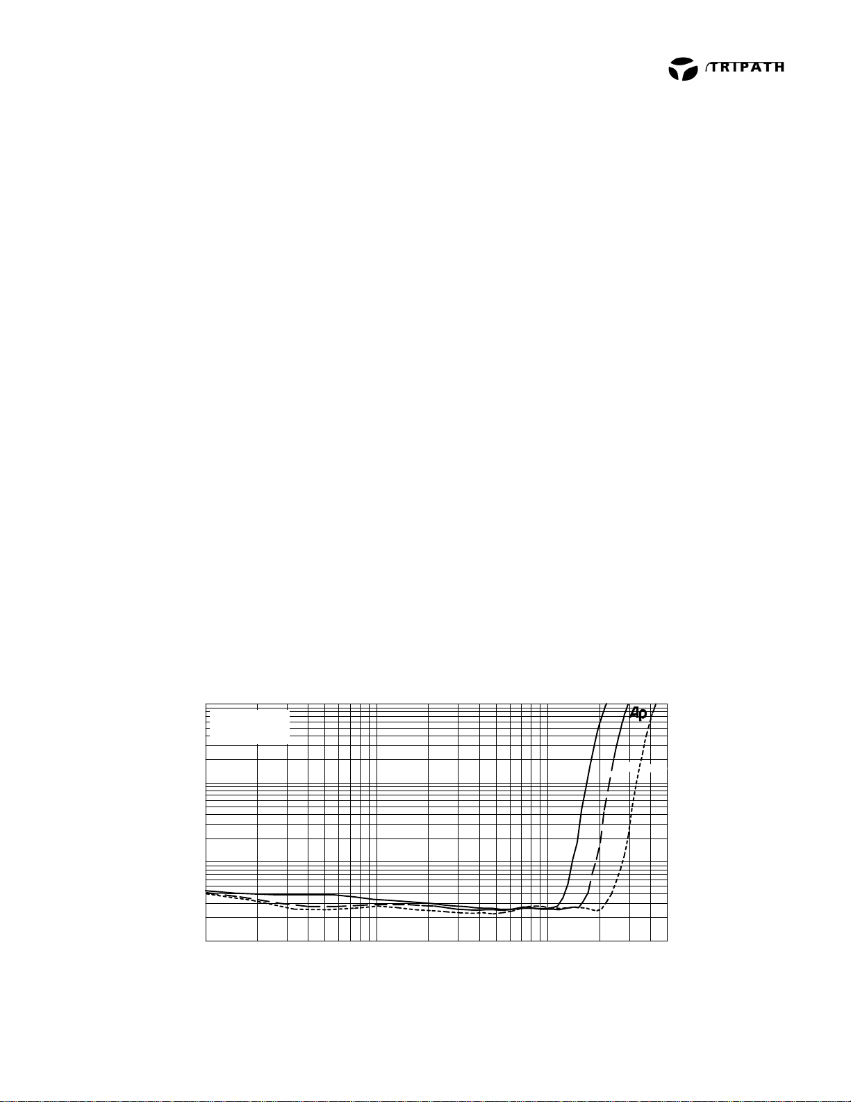
Typical Performance
THD+N versus Output Power versus Supply Voltage
10
f = 1kHz
5
BBM = 80nS
BW = 22Hz - 22kHz
2
1
0.5
0.2
THD+N (%)
0.1
0.05
0.02
0.01
1 5002 5 10 20 50 100 200
R
= 4
Ω
L
Output Power (W)
39V
45V
54V
TA3020, Rev 2.1, 01.01 1
Page 2
TECHNICAL INFORMATION
Absolute Maximum Ratings
(Note 1)
SYMBOL PARAMETER Value UNITS
VPP, VNN Supply Voltage +/- 70 V
V5 Positive 5 V Bias Supply
VN10 Voltage for FET drive VNN+13 V
T
STORE
T
A
TJ Junction Temperature 150º C
ESDHB ESD Susceptibility – Human Body Model (Note 3)
ESDMM ESD Susceptibility – Machine Model (Note 4)
Note 1: Absolute Maximum Ratings indicate limits beyond which damage to the device may occur.
Note 2: This is a target specification. Characterization is still needed to validate this temperature range.
Note 3: Human body model, 100pF discharged through a 1.5KΩ resistor.
Note 4: Machine model, 220pF – 240pF discharged through all pins.
Voltage at Input Pins (pins 12-16, 18, 19-26, 29-33, 37)
Storage Temperature Range -55º to 150º C
Operating Free-air Temperature Range (Note 2) -40º to 85º C
All pins
All pins
See the table below for Operating Conditions.
-0.3V to (V5+0.3V)
6
TBD
TBD
V
V
V
Operating Conditions
(Note 5)
SYMBOL PARAMETER MIN. TYP. MAX. UNITS
VPP, VNN Supply Voltage +/- 15 +/-45 +/- 65 V
V5 Positive 5 V Bias Supply 4.5 5 5.5 V
VN10 Voltage for FET drive (Volts above VNN) 9 10 12 V
Note 5: Recommended Operating Conditions indicate conditions for which the device is functional.
See Electrical Characteristics for guaranteed specific performance limits.
2
TA3020, Rev 2.1, 01.01
Page 3

TECHNICAL INFORMATION
Electrical Characteristics
(Note 6)
TA = 25 °C. See Application/Test Circuit on page 7. Unless otherwise noted, the supply voltage is
VPP=|VNN|=45V.
SYMBOL PARAMETER CONDITIONS MIN. TYP. MAX. UNITS
I
q
I
MUTE
VIH High-level input voltage (MUTE) 3.5 V
VIL Low-level input voltage (MUTE) 1.0 V
VOH High-level output voltage (HMUTE) I
VOL Low-level output voltage (HMUTE) I
V
OFFSET
IOC Over Current Sense Voltage
I
VPPSENSE
V
VPPSENSE
I
VNNSENSE
V
VNNSENSE
Note 6: Minimum and maximum limits are guaranteed but may not be 100% tested.
Quiescent Current
(No load, BBM0=1,BBM1=0,
Mute = 0V)
VPP = +45V
VNN = -45V
V5 = 5V
VN10 = 10V
Mute Supply Current
(No load, Mute = 5V)
VPP = +45V
VNN = -45V
V5 = 5V
VN10 = 10V
= 3mA 4.0 V
OH
= 3mA 0.5 V
OL
Output Offset Voltage No Load, MUTE = Logic low
0.1% R
FBA
, R
FBB
, R
resistors
FBC
TBD TBD 1.0 TBD V
Threshold
VPPSENSE Threshold Currents Over-voltage turn on (muted)
Over-voltage turn off (mute off)
Under-voltage turn off (mute off)
Under-voltage turn on (muted)
Threshold Voltages with
R
VPPSENSE
= XXKΩ
Over-voltage turn on (muted)
Over-voltage turn off (mute off)
Under-voltage turn off (mute off)
Under-voltage turn on (muted)
VNNSENSE Threshold Currents Over-voltage turn on (muted)
Over-voltage turn off (mute off)
Under-voltage turn off (mute off)
Under-voltage turn on (muted)
Threshold Voltages with
R
VNNSENSE
= XXKΩ
Over-voltage turn on (muted)
Over-voltage turn off (mute off)
Under-voltage turn off (mute off)
Under-voltage turn on (muted)
90
90
45
200
1
1
20
1
TBD
TBD
TBD
mA
mA
mA
mA
mA
mA
mA
mA
-TBD TBD mV
TBD
TBD
TBD
TBD
TBD
TBD
TBD
TBD
162
154
TBD
TBD
TBD
TBD
174
169
TBD
TBD
TBD
TBD
79
72
86
77
TBD
TBD
TBD
TBD
TBD
TBD
TBD
TBD
A
µ
A
µ
A
µ
A
µ
V
V
V
V
A
µ
A
µ
A
µ
A
µ
V
V
V
V
TA3020, Rev 2.1, 01.01 3
Page 4

TECHNICAL INFORMATION
Performance Characteristics – Single Ended
TA = 25 °C. Unless otherwise noted, the supply voltage is VPP=|VNN|=45V, the input frequency is
1kHz and the measurement bandwidth is 20kHz. See Application/Test Circuit.
SYMBOL PARAMETER CONDITIONS MIN. TYP. MAX. UNITS
P
Output Power
OUT
THD + N Total Harmonic Distortion Plus
IHF-IM IHF Intermodulation Distortion
SNR Signal-to-Noise Ratio
CS Channel Separation
η
AV Amplifier Gain
A
VERROR
e
NOUT
(continuous RMS/Channel)
Noise
Power Efficiency
Channel to Channel Gain Error
Output Noise Voltage A Weighted, no signal, input shorted,
THD+N = 0.1%, R
R
THD+N = 1%, R
R
= 50W/Channel, RL = 8Ω
P
OUT
19kHz, 20kHz, 1:1 (IHF), R
= 30W/Channel
P
OUT
A Weighted, R
= 275W/Channel
P
OUT
0dBr = 30W, R
= 150W/Channel, RL = 8Ω
P
OUT
P
= 10W/Channel, RL = 4Ω
OUT
See Application / Test Circuit
P
= 10W/Channel, RL = 4Ω
OUT
See Application / Test Circuit
DC offset nulled to zero
= 8Ω
L
= 4Ω
L
= 8Ω
L
= 4Ω
L
= 4Ω,
L
= 8Ω, f = 1kHz
L
= 8Ω
L
100
190
120
220
0.02 %
0.03 %
102 dB
97 dB
95 %
TBD V/V
260
0.5 dB
W
W
W
W
V
µ
4
TA3020, Rev 2.1, 01.01
Page 5

TECHNICAL INFORMATION
TA3020 Pinout
48-pin Dip
(Top View)
VN10
LO2
LO2COM
HO2COM
HO2
OCS2LN
OCS2LP
OCS2HP
OCS2HN
VBOOT2
NC
OCR2
FBKOUT1
FBKGND1
HMUTE
FBKOUT2
DCOMP
FBKGND2
BIASCAP
INV2
OAOUT2
BBM0
BBM1
MUTE
1
2
3
4
5
6
7
8
9
10
11
12
13
14
15
16
17
18
19
20
21
22
23
24
48
LO1
47
LO1COM
46
HO1COM
45
HO1
44
OCS1HN
43
OCS1HP
42
OCS1LP
41
OCS1LN
40
VBOOT1
39
VNN
38
NC
37
OCR1
36
NC
35
V5
34
AGND
33
OCR1
32
REF1
31
OCR2
30
VNNSENSE
29
VPPSENSE
28
AGND
27
V5
26
OAOUT1
25
INV1
TA3020, Rev 2.1, 01.01 5
Page 6

TECHNICAL INFORMATION
Pin Description
Pin
1 VN10 “Floating” supply input for the FET drive circuitry. This voltage must be stable
2,48 LO2, LO1 Low side gate drive output (Channel 2 & 1)
3,47 LO2COM, LO1COM Kelvin connection to source of low-side transistor (Channel 2 & 1)
4,46 HO2COM, HO1COM Kelvin connection to source of high-side transistor (Channel 2 & 1)
5,45 HO2, HO1 High side gate drive output (Channel 2 & 1)
6, 7 OCS2LN, OCS2LP Over Current Sense inputs, Channel 2 low-side
8, 9 OCS2HP, OCS2HN Over Current Sense inputs, Channel 2 high-side
10, 40 VBOOT2, VBOOT1 Bootstrapped voltage to supply drive to gate of high-side FET
12, 31 OCR2 Over-current threshold adjustment (Channel 2)
13, 16 FBKOUT1, FBKOUT2 Switching feedback (Channels 1 & 2)
14, 18 FBKGND1, FBKGND2 Ground Kelvin feedback (Channels 1 & 2)
15 HMUTE Logic Output. A logic high indicates both amplifiers are muted, due to the
17 DCOMP Internal mode selection. This pin must be grounded for proper device
19 BIASCAP Bandgap reference times two (typically 2.5VDC). Used to set the common
20, 25 INV2, INV1 Inverting inputs of Input Stage op amps. (Channels 2 & 1)
21, 26 OAOUT2, OAOUT1 Outputs of Input Stage op amps. (Channels 2 & 1)
22, 23 BBM0, BBM1 Break-before-make timing control to prevent shoot-through in the output FETs.
24 MUTE Logic input. A logic high puts the amplifier in mute mode. Ground pin if not
27, 35 V5 5V power supply input.
28,34 AGND Analog ground.
29 VPPSENSE Positive supply voltage sense input. This pin is used for both over and
30 VNNSENSE Negative supply voltage sense input. This pin is used for both over and under
32 REF Used to set internal bias currents. The pin voltage is typically 1.1V.
33, 37 OCR1 Over-current threshold adjustment (Channel 1)
39 VNN Negative supply voltage.
41, 42 OCS1LN, OCS1LP Over Current Sense inputs, Channel 1 low-side
43, 44 OCS1HP, OCS1HN Over Current Sense inputs, Channel 1 high-side
11, 36,
38
Function
and referenced to VNN.
(Channel 2 & 1)
mute pin state, or a “fault” such as an overcurrent, undervoltage, or
overvoltage condition.
operation.
mode voltage for the input op amps. This pin is not capable of driving external
circuitry.
used. Please refer to the section, Mute Control, in the Application Information.
under voltage sensing for the VPP supply.
voltage sensing for the VNN supply.
NC Not connected (bonded) internally. To minimize coupling between pins, tie
these pins to AGND (pin34).
Description
6
TA3020, Rev 2.1, 01.01
Page 7
TECHNICAL INFORMATION
Application/Test Circuit
26
OAOUT1
C
I
3.3uF
+
V5 (Pin 27)
R
10K
Offset Trim
Circuit
OFA
Ω
R
F
20K
Ω
R
I
49.9K
Ω
R
OFB
499K
Ω
AGND (Pin 28)
C
A
0.1uF
(Pin 28)
5V
(Pin 28)
R
REF
8.25K
1%
Ω,
INV1
R
OFB
499K
C
OF
0.1uF
BIASCAP
MUTE
REF
25
AGND
Ω
2.5V
19
24
32
-
+
V5
200K
V5
TA3020
Processing
Modulation
Ω
OCS1HP
43
C
OCR
(Pin 28)
AGND
150pF
0.01
R
G
5.6, 1W
R
G
5.6, 1W
0.01
R
OCR
20K
C
FB
AGND (Pin 28)
OCS1HN
44
VBOOT1
40
HO1
45
46
HO1COM
VN10
LO1
&
48
47
42
41
37
33
LO1COM
OCS1LP
OCS1LN
OCR1
OCR1
220pF
FBKOUT1
13
FBKGND1
14
HMUTE
15
1W
Ω,
1W
Ω,
Ω
R
S
Q
O
Q
O
R
S
V5 (Pin 27)
R
FBA
1K
Ω
*R
FBB
1.07K
Ω
C
S
C
HBR
0.1uF
0.1uF
R
FBA
1K
*R
1.07K
Ω
*R
13.3K
FBB
D
B
Ω
MUR120
R
B
C
B
0.1uF
L
O
10uH
C
S
0.1uF
FBC
Ω
*R
13.3K
250
VN10
FBC
Ω
+
Ω
+
C
BAUX
47uF
C
O
0.22uF
+
C
S
330uF
C
S
330uF
VPP
R
Z
20
C
0.22uF
2W
Ω,
R
Z
4Ω or 8
L
Ω
VNN
C
3.3uF
V5 (Pin 27)
R
10K
Offset Trim
Circuit
VNN
VPP
*R
V5
*R
V5
(Pin 28)
I
+
R
49.9K
OFA
Ω
AGND (Pin 28)
5V
*R
VNN1
*R
VPP1
VNN2
1.35M
450K
VPP1
I
450K
450K
20K
R
OFB
499K
Ω,
Ω
Ω,
Ω,
Ω,
R
Ω
Ω
0.1uF
0.1uF
1%
1%
1%
1%
OAOUT2
F
DCOMP
C
S
C
S
21
V5
20
INV2
-
R
OFB
499K
C
0.1uF
BBM0
BBM1
+
AGND
Ω
OF
22
23
17
27
V5
28
AGND
35
V5
34
AGND
30
VNNSENSE
29
VPPSENSE
11
NC
F. BEAD
* The values of these components must be
adjusted based on supply voltage range.
See Application Information.
Processing
&
Modulation
Analog Ground
Power Ground
VN10
VN10
VNN
NC
NC
7
8
10
5
4
2
3
7
8
12
31
16
18
1
39
38
36
OCS2HP
OCS2HN
VBOOT2
HO2
HO2COM
LO2
LO2COM
OCS2LP
OCS2LN
OCR2
OCR2
C
OCR
220pF
AGND
(Pin 28)
FBKOUT2
FBKGND2
C
0.1uF,35V
VNN
VNN
270pF
SW
0.01
Ω,
R
G
5.6, 1W
R
G
5.6, 1W
0.01
Ω,
R
OCR
20K
C
FB
AGND (Pin 28)
VN10
R
S
1W
Q
O
Q
O
R
S
1W
V5 (Pin 27)
Ω
*R
1.07K
C
0.1uF
S
D
MUR120
B
VN10
R
250
Ω
B
+
C
B
C
HBR
0.1uF
0.1uF
L
O
10uH
C
S
R
FBA
1K
Ω
FBB
0.1uF
R
FBA
1K
Ω
*R
FBC
13.3K
Ω
*R
*R
1.07K
Ω
FBC
13.3K
FBB
Ω
Ω
+
C
BAUX
47uF
C
0.22uF
+
C
330uF
O
C
S
330uF
VPP
S
R
Z
20
2W
Ω,
C
0.22uF
R
Z
4Ω or 8
L
Ω
VNN
TA3020, Rev 2.1, 01.01 7
Page 8

p
TECHNICAL INFORMATION
External Components Description
Components Description
R
Inverting input resistance to provide AC gain in conjunction with RF. This input is
I
RF Feedback resistor to set AC gain in conjunction with RI. Please refer to the Amplifier
CI AC input coupling capacitor which, in conjunction with RI, forms a highpass filter at
R
FBA
R
Feedback divider resistor connected to AGND. This value of this resistor depends
FBB
R
Feedback resistor connected from either the OUT1(OUT2) to FBKOUT1(FBKOUT2)
FBC
CFB Feedback delay capacitor that both lowers the idle switching frequency and filters
R
Potentiometer used to manually trim the DC offset on the output of the TA3020.
OFA
R
Resistor that limits the manual DC offset trim range and allows for more precise
OFB
R
Bias resistor. Locate close to pin 32 and ground at pin 28.
REF
CA BIASCAP decoupling capacitor. Should be located close to pin 19 and grounded at
DB Bootstrap diode. This diode charges up the bootstrap capacitors when the output is
CB High frequency bootstrap capacitor, which filters the high side gate drive supply.
C
BAUX
RB Bootstrap resistor that limits C
CSW VN10 generator filter capacitors. The high frequency capacitor (0.1uF) must be
CS Supply decoupling for the power supply pins. For optimum performance, these
biased at the BIASCAP voltage (approximately 2.5VDC).
Gain paragraph, in the Application Information section.
.
)CR2(1f
π=
IIC
Feedback divider resistor connected to V5. This resistor is normally set at 1kΩ.
on the supply voltage setting and helps set the TA3020 gain in conjunction with R
R
F, RFBA,
and R
. Please see the Modulator Feedback Design paragraphs in the
FBC
Application Information Section.
or speaker ground to FBKGND1(FBKGND2). The value of this resistor depends on
the supply voltage setting and helps set the TA3020 gain in conjunction with R
R
FBA,
, and R
. It should be noted that the resistor from OUT1(OUT2) to
FBB
FBKOUT1(FBKOUT2) must have a power rating of greater than
Please see the Modulator Feedback Design paragraphs in the Application
Information Section.
very high frequency noise from the feedback signal, which improves amplifier
performance. The value of C
so that the idle switching difference is greater than 40kHz. Please refer to the
Application / Test Circuit.
adjustment.
pin 28.
low (at VNN) to drive the high side gate circuitry. A fast or ultra fast recovery diode
is recommended for the bootstrap circuitry. In addition, the bootstrap diode must be
able to sustain the entire VPP-VNN voltage. Thus, for most applications, a 150V (or
greater) diode should be used.
This capacitor must be located as close to pin 40 (VBOOT1) or pin10 (VBOOT2) for
reliable operation. The “negative” side of C
HO1COM (pin 46) or HO2COM (pin 4). Please refer to the Application / Test Circuit.
Bulk bootstrap capacitor that supplements C
in a reduction in the average switching frequency.
(bootstrap supply charging).
located close to pin 1 (VN10) to maximize device performance.
com
onents should be located close to the TA3020 and returned to their respective
(Refer to the Application/Test Circuit)
should be offset between channel 1 and channel 2
FB
should be connected directly to the
B
during “clipping” events, which result
B
charging current during TA3020 power up
BAUX
DISS
=
2
I, RF,
FBC
I,
.
)(2RVPPP
8
TA3020, Rev 2.1, 01.01
Page 9

TECHNICAL INFORMATION
g
ground as shown in the Application/Test Circuit.
R
VNN1
R
VNN2
R
VPP1
R
VPP2
R
S
R
OCR
C
OCR
C
Supply decoupling for the high current Half-bridge supply pins. These components
HBR
RG Gate resistor, which is used to control the MOSFET rise/ fall times. This resistor
CZ Zobel capacitor, which in conjunction with RZ, terminates the output filter at high
RZ Zobel resistor, which in conjunction with CZ, terminates the output filter at high
LO Output inductor, which in conjunction with CO, demodulates (filters) the switching
Main overvoltage and undervoltage sense resistor for the negative supply (VNN).
Please refer to the Electrical Characteristics Section for the trip points as well as the
hysteresis band. Also, please refer to the Over / Under-voltage Protection section in
the Application Information for a detailed discussion of the internal circuit operation
and external component selection.
Secondary overvoltage and undervoltage sense resistor for the negative supply
(VNN). This resistor accounts for the internal V
resistor value should be three times that of R
VNN1
NNSENSE
bias of 1.25V. Nominal
. Please refer to the Over / Undervoltage Protection section in the Application Information for a detailed discussion of
the internal circuit operation and external component selection.
Main overvoltage and undervoltage sense resistor for the positive supply (VPP).
Please refer to the Electrical Characteristics Section for the trip points as well as the
hysteresis band. Also, please refer to the Over / Under-voltage Protection section in
the Application Information for a detailed discussion of the internal circuit operation
and external component selection.
Secondary overvoltage and undervoltage sense resistor for the positive supply
(VPP). This resistor accounts for the internal V
resistor value should be equal to that of R
VPP1
PPSENSE
. Please refer to the Over / Under-
bias of 2.5V. Nominal
voltage Protection section in the Application Information for a detailed discussion of
the internal circuit operation and external component selection.
Over-current sense resistor. Please refer to the section, Setting the Over-current
Threshold, in the Application Information for a discussion of how to choose the value
of R
to obtain a specific current limit trip point.
S
Over-current “trim” resistor, which, in conjunction with R
, sets the current trip point.
S
Please refer to the section, Setting the Over-current Threshold, in the Application
Information for a discussion of how to calculate the value of R
OCR
.
Over-current filter capacitor, which filters the overcurrent signal at the OCR pins to
account for the half-wave rectified current sense circuit internal to the TA3020. A
typical value for this component is 220pF. In addition, this component should be
located near pin 31 or pin 33 as possible.
must be located as close to the device as possible to minimize supply overshoot and
maximize device reliability. These capacitors should have good high frequency
performance including low ESR and low ESL. In addition, the capacitor rating must
be twice the maximum VPP voltage.
serves to dampen the parasitics at the MOSFET gates, which, in turn, minimizes
ringing and output overshoots. The typical power rating is 1 watt.
frequencies. Use a high quality film capacitor capable of sustaining the ripple current
caused by the switching outputs.
frequencies. The combination of R
and CZ minimizes peaking of the output filter
Z
under both no load conditions or with real world loads, including loudspeakers which
usually exhibit a rising impedance with increasing frequency. Depending on the
program material, the power rating of R
may need to be adjusted. The typical
Z
power rating is 2 watts.
waveform into an audio si
nal. Forms a second order filter with a cutoff frequency
TA3020, Rev 2.1, 01.01 9
Page 10

TECHNICAL INFORMATION
of
C
O
Output capacitor, which, in conjunction with L
waveform into an audio signal. Forms a second order low-pass filter with a cutoff
π=
frequency of
a high quality film capacitor capable of sustaining the ripple current caused by the
switching outputs.
and a quality factor of
)CL2(1f
OOC
and a quality factor of
π=
)CL2(1f
OOC
=
, demodulates (filters) the switching
O
.
CLCRQ
OOOL
.
Use
=
CLCRQ
OOOL
10
TA3020, Rev 2.1, 01.01
Page 11

TECHNICAL INFORMATION
0
k
Typical Performance
10
f = 1kHz
5
BBM = 80nS
Vs = +28V
BW = 22Hz - 22kHz
2
1
0.5
0.2
THD+N (%)
0.1
0.05
0.02
0.01
+0
-10
-20
-30
-40
-50
-60
-70
FFT (dBr)
-80
-90
-100
-110
-120
20 20k50 100 200 500 1k 2k 5k 10k
2 20
19kHz, 20kHz, 1:1
Pout = 40W/Channel
0dBr = 12.65Vrms
Vs = +28V
BW = 22Hz - 22kHz
THD+N versus Output Power
RL = 8
Ω
5 10 20 50 100
Output Power (W)
Intermodulation Performance
R
= 4
Ω
L
Frequency (Hz)
-40
-45
Pout = 40W/Channel @ 4
Pout = 20W/Channel @ 8
-50
V
= +28V
S
-55
BW = 22Hz - 22kHz
-60
-65
-70
-75
-80
-85
-90
Channel Separation (dBr)
-95
-100
-105
-110
-115
-120
20 20k50 100 200 500 1k 2k 5k 10k
Channel Separation versus Frequency
Ω
Ω
RL = 4
Ω
R
= 8
Ω
L
Frequency (Hz)
RL = 4
100
90
80
Ω
70
60
50
40
Efficiency (%)
30
20
10
RL = 8
Ω
RL = 4
Ω
f = 1kHz
BBM = 80nS
Vs = +28V
THD+N = <10%
0
0 20 40 60 80 100 120
Output Power (W)
Efficiency versus Output Power
Intermodulation Performance
R
= 8
Ω
+0
-10
19kHz, 20kHz, 1:1
Pout = 20W/Channel
0dBr = 12.65Vrms
-20
Vs = +28V
BW = 22Hz - 22kHz
-30
-40
-50
-60
FFT (dBr)
-70
-80
-90
-100
-110
-120
20 20k50 100 200 500 1k 2k 5k 10k
-70
VS = +28V
-75
BBM = 80nS
16K FFT
Fs = 48kHz
-80
BW = 22Hz - 22kHz
-85
-90
-95
Noise FFT (dBV)
-100
-105
-110
-115
-120
20 20
50 100 200 500 1k 2k 5k 10k
L
Frequency (Hz)
Noise Floor
Frequency (Hz)
TA3020, Rev 2.1, 01.01 11
Page 12

0
0
TECHNICAL INFORMATION
Typical Performance
THD+N versus Frequency versus Break Before Make
10
Pout = 40W/Channel
5
Vs = +28V
BW = 22Hz - 22kHz
2
1
0.5
0.2
THD+N (%)
0.1
0.05
0.02
0.01
20 20k50 100 200 500 1k 2k 5k 10k
R
= 4
L
Frequency (Hz)
Ω
BBM = 120nS
BBM = 80nS
THD+N versus Frequency versus Break Before Make
10
Pout = 20W/Channel
Vs = +28V
5
BW = 22Hz - 22kHz
2
1
0.5
0.2
THD+N (%)
0.1
0.05
0.02
0.01
20 20k50 100 200 500 1k 2k 5k 10k
R
= 8
Ω
L
Frequency (Hz)
BBM = 120nS
BBM = 80nS
THD+N versus Frequency versus Bandwidth
10
Pout = 40W/Channel
Vs = +28V
5
BBM = 80nS
2
1
0.5
0.2
0.1
THD+N (%)
0.05
0.02
0.01
20 20k50 100 200 500 1k 2k 5k 10k
R
= 4
Ω
L
BW = 30kHz
BW = 22kHz
Frequency (Hz)
10
f = 1kHz
5
BBM = 80nS
BW = 22Hz - 22kHz
2
1
0.5
0.2
THD+N (%)
0.1
0.05
THD+N versus Output Power versus Supply Voltage
= 4
R
Ω
L
23V
28V
35V
THD+N versus Frequency versus Bandwidth
10
Pout = 20W/Channel
Vs = +28V
5
BBM = 80nS
2
1
0.5
0.2
THD+N (%)
0.1
0.05
0.02
0.01
20 20k50 100 200 500 1k 2k 5k 10k
BW = 30kHz
BW = 22kHz
R
= 8
Ω
L
Frequency (Hz)
10
f = 1kHz
BBM = 80nS
5
BW = 22Hz - 22kHz
2
1
0.5
0.2
THD+N (%)
0.1
0.05
THD+N versus Output Power versus Supply Voltage
= 8
R
Ω
L
23V
28V
35V
0.02
0.01
1 20
2 5 10 20 50 100
Output Power (W)
12
0.02
0.01
2 20
5 10 20 50 100
Output Power (W)
TA3020, Rev 2.1, 01.01
Page 13

TECHNICAL INFORMATION
0
Typical Performance
10
f = 1kHz
BBM = 80nS
5
Vs = +45V
BW = 22Hz - 22kHz
2
1
0.5
0.2
THD+N (%)
0.1
0.05
0.02
0.01
2 50
THD+N versus Output Power
RL = 8
Ω
5 10 20 50 100 200
Output Power (W)
Intermodulation Performance
R
= 4
+0
19kHz, 20kHz, 1:1
-10
Pout = 60W/Channel
0dBr = 15.5Vrms
-20
Vs = +45V
BW = 22Hz - 22kHz
-30
-40
-50
-60
-70
FFT (dBr)
-80
-90
-100
-110
-120
20 20k50 100 200 500 1k 2k 5k 10k
Ω
L
Frequency (Hz)
RL = 4
100
80
Efficiency versus Output Power
Ω
RL = 8
RL = 4
Ω
Ω
60
Efficiency (%)
40
f = 1kHz
20
0
0 50 100 150 200 250 300
BBM = 80nS
Vs = +45V
THD+N <10%
Output Power (W)
Intermodulation Performance
R
= 8
Ω
+0
19kHz, 20kHz, 1:1
-10
Pout = 30W/Channel
0dBr = 15.5Vrms
-20
Vs = +45V
BW = 22Hz - 22kHz
-30
-40
-50
-60
FFT (dBr)
-70
-80
-90
-100
-110
-120
20 20k50 100 200 500 1k 2k 5k 10k
L
Frequency (Hz)
-40
Pout = 60W/Channel @ 4
-45
Pout = 30W/Channel @ 8
-50
= +45V
V
S
BW = 22Hz - 22kHz
-55
-60
-65
-70
-75
-80
-85
-90
Channel Separation (dBr)
-95
-100
-105
-110
-115
-120
20 20k50 100 200 500 1k 2k 5k 10k
Ω
Ω
R
= 4
Ω
L
= 8
R
Ω
L
Frequency (Hz)
Channel Separation versus Frequency
-70
VS = +/-45V
BBM = 80nS
-75
16kFFT
S
F
= 48kHz
BW = 22Hz-22kHz
-80
-85
-90
-95
-100
Amplitude (dBV)
-105
-110
-115
-120
20 20k50 100 200 500 1k 2k 5k
Noise Floor
Frequency (Hz)
10k
TA3020, Rev 2.1, 01.01 13
Page 14

0
0
TECHNICAL INFORMATION
Typical Performance
THD+N versus Frequency versus Break Before Make
10
Pout = 60W/Channel
Vs = +45V
5
BW = 22Hz - 22kHz
2
1
0.5
THD+N (%)
0.2
0.1
0.05
0.02
0.01
20 20k50 100 200 500 1k 2k 5k 10k
R
= 4
Ω
L
Frequency (Hz)
BBM = 120nS
BBM = 80nS
THD+N versus Frequency versus Break Before Make
10
Pout = 30W/Channel
Vs = +45V
5
BW = 20Hz - 22kHz
2
1
0.5
0.2
THD+N (%)
0.1
0.05
0.02
0.01
20 20k50 100 200 500 1k 2k 5k 10k
R
= 8
Ω
L
Frequency (Hz)
BBM = 120nS
BBM = 80nS
THD+N versus Frequency versus Bandwidth
10
Pout = 60W/Channel
Vs = +45V
5
BBM = 80nS
2
1
0.5
0.2
THD+N (%)
0.1
0.05
0.02
0.01
20 20k50 100 200 500 1k 2k 5k 10k
THD+N versus Output Power versus Supply Voltage
10
f = 1kHz
5
BBM = 80nS
BW = 22Hz - 22kHz
2
1
0.5
R
= 4
Ω
L
Frequency (Hz)
= 4
R
L
BW = 30kHz
BW = 22kHz
Ω
39V
45V
54V
THD+N versus Frequency versus Bandwidth
10
Pout = 30W/Channel
Vs = +45V
5
BBM = 80nS
2
1
0.5
0.2
THD+N (%)
0.1
0.05
0.02
0.01
20 20k50 100 200 500 1k 2k 5k 10k
R
= 8
Ω
L
BW = 30kHz
BW = 22kHz
Frequency (Hz)
10
f = 1kHz
5
BBM = 80nS
BW = 22Hz - 22kHz
2
1
0.5
THD+N versus Output Power versus Supply Voltage
= 8
R
Ω
L
39V
45V
54V
0.2
THD+N (%)
0.1
0.05
0.02
0.01
1 50
2 5 10 20 50 100 200
Output Power (W)
14
0.2
THD+N (%)
0.1
0.05
0.02
0.01
2 50
5 10 20 50 100 200
Output Power (W)
TA3020, Rev 2.1, 01.01
Page 15

TECHNICAL INFORMATION
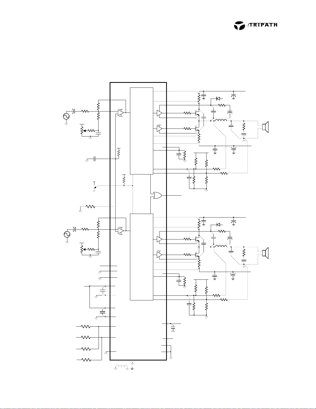
Application Information
Figure 1 is a simplified diagram of one channel (Channel 1) of a TA3020 amplifier to assist in
understanding its operation.
22
I
R
OFB
R
5V
C
R
F
C
A
5V
REF
VNNSENSE
VPPSENSE
S
BBM0
BBM1
OAOUT1
INV1
R
OFB
C
OF
BIASCAP
MUTE
REF
AGND
OCS1HP
VN10
VN10
VNN
33,37
43
44
40
45
46
48
47
42
41
13
14
15
1
39
OCS1HN
VBOOT1
HO1
HO1COM
LO1
LO1COM
OCS1LP
OCS1LN
OCR1
C
OCR
FBKOUT1
FBKGND1
HMUTE
VNN
VNN
S
Q
R
O
G
C
Q
R
O
G
R
S
V5
R
OCR
R
FBA
C
FB
R
FBB
VN10
C
SW
R
C
B
0.1uF
HBR
OUTPUT
C
S
R
FBA
R
FBC
R
FBB
D
C
B
S
R
23
26
V5
25
-
+
AGND
Processing
&
Modulation
2.5V
19
V5
24
32
30
OVER/
UNDER
VOLTAGE
29
DETECTION
V5
27,35
28,34
F. BEAD
CURRENT
DETECTION
CURRENT
DETECTION
Analog Ground
Power Ground
OVER
OVER
VN10
B
FILTER
R
FBC
VPP
+
C
BAUX
R
L
VNN
R
C
I
+
R
Offset Trim
Circuit
V5
OFA
*R
VNN
VPP
VNN1
*R
VPP1
*R
VNN2
V5
*R
VPP1
V5
Figure 1: Simplified TA3020 Amplifier
TA3020 Basic Amplifier Operation
The audio input signal is fed to the processor internal to the TA3020, where a switching pattern is
generated. The average idle (no input) switching frequency is approximately 700kHz. With an input
signal, the pattern is spread spectrum and varies between approximately 200kHz and 1.5MHz
depending on input signal level and frequency. Complementary copies of the switching pattern are
level-shifted by the MOSFET drivers and output from the TA3020 where they drive the gates (HO1
and LO1) of external power MOSFETs that are connected as a half bridge. The output of the half
bridge is a power-amplified version of the switching pattern that switches between VPP and VNN.
This signal is then low-pass filtered to obtain an amplified reproduction of the audio input signal.
The processor portion of the TA3020 is operated from a 5-volt supply. In the generation of the
switching patterns for the output MOSFETs, the processor inserts a “break-before-make” dead time
between the turn-off of one transistor and the turn-on of the other in order to minimize shoot-through
currents in the MOSFETs. The dead time can be programmed by setting the break-before-make
control bits, BBM1 and BBM0. Feedback information from the output of the half-bridge is supplied to
TA3020, Rev 2.1, 01.01 15
Page 16

TECHNICAL INFORMATION
the processor via FBKOUT1. Additional feedback information to account for ground bounce is
supplied via FBKGND1.
The MOSFET drivers in the TA3020 are operated from voltages obtained from VN10 and LO1COM
for the low-side driver, and VBOOT1 and HO1COM for the high-side driver. VN10 must be a
regulated 10V above VNN.
N-Channel MOSFETs are used for both the top and bottom of the half bridge. The gate resistors, R
,
G
are used to control MOSFET slew rate and thereby minimize voltage overshoots.
Circuit Board Layout
The TA3020 is a power (high current) amplifier that operates at relatively high switching frequencies.
The output of the amplifier switches between VPP and VNN at high speeds while driving large
currents. This high-frequency digital signal is passed through an LC low-pass filter to recover the
amplified audio signal. Since the amplifier must drive the inductive LC output filter and speaker
loads, the amplifier outputs can be pulled above the supply voltage and below ground by the energy
in the output inductance. To avoid subjecting the TA3020 to potentially damaging voltage stress, it
is critical to have a good printed circuit board layout. It is recommended that Tripath’s layout and
application circuit be used for all applications and only be deviated from after careful analysis of the
effects of any changes. Please refer to the TA3020 evaluation board document, EB-TA3020,
available on the Tripath website, at www.tripath.com.
The following components are important to place near their associated TA3020 pins and are ranked
in order of layout importance, either for proper device operation or performance considerations.
The capacitors C
-
provide high frequency bypassing of the amplifier power supplies and
HBR
will serve to reduce spikes across the supply rails. Please note that both mosfet halfbridges must be decoupled separately. In addition, the voltage rating for C
should be
HBR
at least 150V as this capacitor is exposed to the full supply range, VPP-VNN.
C
-
removes very high frequency components from the amplifier feedback signals and
FB
lowers the output switching frequency by delaying the feedback signals. In addition, the
value of C
is different for channel 1 and channel 2 to keep the average switching
FB
frequency difference greater than 40kHz. This minimizes in-band audio noise.
To minimize noise pickup and minimize THD+N, R
-
should be located as close to the
FBC
TA3020 as possible. Make sure that the routing of the high voltage feedback lines is kept
far away from the input op amps or significant noise coupling may occur. It is best to
shield the high voltage feedback lines by using a ground plane around these traces as well
as the input section.
C
, CSW provides high frequency bypassing for the VN10 and bootstrap supplies. Very
-
B
high currents are present on these supplies.
In general, to enable placement as close to the TA3020, and minimize PCB parasitics, the
capacitors listed above should be surface mount types, located on the “solder” side of the board.
Some components are not sensitive to location but are very sensitive to layout and trace routing.
16
TA3020, Rev 2.1, 01.01
Page 17

TECHNICAL INFORMATION
To maximize the damping factor and reduce distortion and noise, the modulator feedback
-
connections should be routed directly to the pins of the output inductors. L
to the EB-TA3020This was done on the EB-TA3020 for additional information.
The output filter capacitor, C
-
, and zobel capacitor, CZ, should be star connected with the
O
load return. The output ground feedback signal should be taken from this star point.
The modulator feedback resistors, R
-
FBA
, R
, and R
FBB
should all be grounded and
FBC,
attached to 5V together. These connections will serve to minimize common mode noise
via the differential feedback. Please refer to the EB-TA3020 evaluation board for more
information.
TA3020 Grounding
Proper grounding techniques are required to maximize TA3020 functionality and performance.
Parametric parameters such as THD+N, Noise Floor and Crosstalk can be adversely affected if
proper grounding techniques are not implemented on the PCB layout. The following discussion
highlights some recommendations about grounding both with respect to the TA3020 as well as
general “audio system” design rules.
The TA3020 is divided into two sections: the input section, which spans pin 12 through pin 37, and
the output (high voltage) section, which spans pin 1 through pin 10 and pin 39 through pin 48. On
the TA3020 evaluation board, the ground is also divided into distinct sections, one for the input and
one for the output. To minimize ground loops and keep the audio noise floor as low as possible, the
input and output ground must be only connected at a single point. Depending on the system design,
the single point connection may be in the form of a ferrite bead or a PCB trace.
The analog grounds, pin 28 and pin 34 must be connected locally at the TA3020 for proper device
functionality. The ground for the V5 power supply should connect directly to pin 28. Additionally, any
external input circuitry such as preamps, or active filters, should be referenced to pin 28.
For the power section, Tripath has traditionally used a “star” grounding scheme. Thus, the load
ground returns and the power supply decoupling traces are routed separately back to the power
supply. In addition, any type of shield or chassis connection would be connected directly to the
ground star located at the power supply. These precautions will both minimize audible noise and
enhance the crosstalk performance of the TA3020.
The TA3020 incorporates a differential feedback system to minimize the effects of ground bounce
and cancel out common mode ground noise. As such, the feedback from the output ground for each
channel needs to be properly sensed. This can be accomplished by connecting the output ground
“sensing” trace directly to the star formed by the output ground return, output capacitor, C
zobel capacitor, C
. Refer to the Application / Test Circuit for a schematic description.
Z
TA3020 Amplifier Gain
The gain of the TA3020 is the product of the input stage gain and the modulator gain. Please refer
to the sections, Input Stage Design, and Modulator Feedback Design, for a complete explanation of
how to determine the external component values.
. Please refer
O
, and the
O
TA3020, Rev 2.1, 01.01 17
Page 18

TECHNICAL INFORMATION
A* AA
=
MODULATORV EVINPUTSTAG VTA3020
R
F
A
VTA3020
−≈
R
I
+
R*R
FBBFBA
)R(R*R
FBBFBAFBC
1
+
For example, using a TA3020 with the following external components,
R
R
R
= 20kΩ
I
R
= 20kΩ
F
R
= 1kΩ
FBA
= 1.13kΩ
FBB
= 9.09kΩ
FBC
A
VTA3020
20k Ω
−≈
49.9k Ω
)1.07k(1.0k Ω*13.3k Ω
1.07k Ω*1.0k Ω
Ω+
10.71- 1
=
+
V
V
Input Stage Design
The TA3020 input stage is configured as an inverting amplifier, allowing the system designer
flexibility in setting the input stage gain and frequency response. Figure 2 shows a typical
application where the input stage is a constant gain inverting amplifier. The input stage gain should
be set so that the maximum input signal level will drive the input stage output to 4Vpp.
TA3020
OAOUT1
V5
-
+
AGND
V5
+
-
INPUT1
INPUT2
CI
RF
RI
CI AGND
INV1
BIASCAP
INV2
OAOUT2
RF
RI
Figure 2: Input Stage
The gain of the input stage, above the low frequency high pass filter point, is that of a simple
inverting amplifier:
R
F
A
EVINPUTSTAG
−=
R
I
18
TA3020, Rev 2.1, 01.01
Page 19

TECHNICAL INFORMATION
Input Capacitor Selection
C
can be calculated once a value for RIN has been determined. CIN and RIN determine the input
IN
low-frequency pole. Typically this pole is set at 10Hz. C
is calculated according to:
IN
C
= 1 / (2π x FP x RIN)
IN
where: R
= Input resistor value in ohms
IN
F
= Input low frequency pole (typically 10Hz)
P
Modulator Feedback Design
The modulator converts the signal from the input stage to the high-voltage output signal. The
optimum gain of the modulator is determined from the maximum allowable feedback level for the
modulator and maximum supply voltages for the power stage. Depending on the maximum supply
voltage, the feedback ratio will need to be adjusted to maximize performance. The values of R
R
FBB
and R
(see explanation below) define the gain of the modulator. Once these values are
FBC
FBA
chosen, based on the maximum supply voltage, the gain of the modulator will be fixed even with as
the supply voltage fluctuates due to current draw.
For the best signal-to-noise ratio and lowest distortion, the maximum modulator feedback voltage
should be approximately 4Vpp. This will keep the gain of the modulator as low as possible and still
allow headroom so that the feedback signal does not clip the modulator feedback stage.
Figure 3 shows how the feedback from the output of the amplifier is returned to the input of the
modulator. The input to the modulator (FBKOUT1/FBKGND1 for channel 1) can be viewed as inputs
to an inverting differential amplifier. R
and R
scales the large OUT1/OUT2 signal to down to 4Vpp.
FBC
FBA
and R
bias the feedback signal to approximately 2.5V
FBB
,
1/2 TA3020
V5
RFBA
RFBA
RFBB
RFBC
RFBC
OUT1
OUT 1 GROUND
Processing
&
Modulation
FBKOUT1
FBKGND1
RFBB
AGND
Figure 3: Modulator Feedback
TA3020, Rev 2.1, 01.01 19
Page 20

TECHNICAL INFORMATION
The modulator feedback resistors are:
FBA
VPP*R
R
FBA
FBB
=
1Ktypically specified, UserR
Ω=
4)-(VPP
VPP*R
R
FBA
FBC
=
4
A
MODULATOR-V
≈
+
R*R
FBBFBA
1
+
)R(R*R
FBBFBAFBC
The above equations assume that VPP=|VNN|.
For example, in a system with VPP
=52V and VNN
MAX
MAX
=-52V,
R
R
R
= 1kΩ, 1%
FBA
= 1.08kΩ, use 1.07kΩ, 1%
FBB
= 13.0kΩ, use 13.3kΩ, 1%
FBC
The resultant modulator gain is:
)1.07k(1.0k Ω*13.3k Ω
A
MODULATOR-V
≈
Ω+
26.73V/V 1
=+
1.07k Ω*1.0k Ω
Mute
When a logic high signal is supplied to MUTE, both amplifier channels are muted (both high- and
low-side transistors are turned off). When a logic level low is supplied to MUTE, both amplifiers are
fully operational. There is a delay of approximately 200 milliseconds between the de-assertion of
MUTE and the un-muting of the TA3020.
Turn-on & Turn-off Noise
If turn-on or turn-off noise is present in a TA3020 amplifier, the cause is frequently due to other
circuitry external to the TA3020. While the TA3020 has circuitry to suppress turn-on and turn-off
transients, the combination of the power supply and other audio circuitry with the TA3020 in a
particular application may exhibit audible transients. One solution that will completely eliminate turnon and turn-off pops and clicks is to use a relay to connect/disconnect the amplifier from the
speakers with the appropriate timing at power on/off. The relay can also be used to protect the
speakers from a component failure (e.g. shorted output MOSFET), which is a protection mechanism
that some amplifiers have. Circuitry external to the TA3020 would need to be implemented to detect
these failures.
DC Offset
While the DC offset voltages that appear at the speaker terminals of a TA3020 amplifier are typically
small, Tripath recommends that any offsets during operation be nulled out of the amplifier with a
circuit like the one shown connected to IN1 and IN2 in the Test/Application Circuit.
20
TA3020, Rev 2.1, 01.01
Page 21

TECHNICAL INFORMATION
It should be noted that the DC voltage on the output of a TA3020 amplifier with no load in mute will
not be zero. This offset does not need to be nulled. The output impedance of the amplifier in mute
mode is approximately 10KΩ. This means that the DC voltage drops to essentially zero when a
typical load is connected.
and R
(measured via OCS1HP,
S
and R
S
are used to set the over-current threshold. The OCS pins must be
OCR
becomes greater than V
OCR
(approximately 1.0V) the TA3020 will
TOC
determine the value of the over-current threshold, ISC:
OCR
= 3580 x (V
SC
R
= (3580 x V
OCR
TOC
– I
TOC
* R
BIAS
)/(I
* RS+3580 * I
SC
OCR
)/(R
OCR
* RS)
BIAS
)
where:
and R
S
= Over-current sense threshold voltage (See Electrical Characteristics Table)
V
TOC
are in Ω
OCR
= 1.0V typically
I
= 20uA
BIAS
of 30A, R
SC
can be used to adjust for a particular over-current threshold using one of these
OCR
.
S
= 9.63KΩ and RS will be 10mΩ.
OCR
HMUTE
The HMUTE pin is a 5V logic output that indicates various fault conditions within the device. These
conditions include: over-current, overvoltage and undervoltage. The HMUTE output is capable of
directly driving an LED through a series 2kΩ resistor.
Over-current Protection
The TA3020 has over-current protection circuitry to protect itself and the output transistors from
short-circuit conditions. The TA3020 uses the voltage across a resistor R
OCS1HN, OCS1LP and OCS1LN) that is in series with each output MOSFET to detect an overcurrent condition. R
Kelvin connected for proper operation. See “Circuit Board Layout” in Application Information for
details.
When the voltage across R
shut off the output stages of its amplifiers. The occurrence of an over-current condition is latched in
the TA3020 and can be cleared by toggling the MUTE input or cycling power.
Setting Over-current Threshold
R
S
I
R
For example, to set an I
As high-wattage resistors are usually only available in a few low-resistance values (10mΩ, 25mΩ
and 50mΩ), R
values for R
Over- and Under-Voltage Protection
The TA3020 senses the power rails through external resistor networks connected to VNNSENSE
and VPPSENSE. The over- and under-voltage limits are determined by the values of the resistors in
the networks, as described in the table “Test/Application Circuit Component Values”. If the supply
voltage falls outside the upper and lower limits determined by the resistor networks, the TA3020
shuts off the output stages of the amplifiers. The removal of the over-voltage or under-voltage
TA3020, Rev 2.1, 01.01 21
Page 22

TECHNICAL INFORMATION
condition returns the TA3020 to normal operation. Please note that trip points specified in the
Electrical Characteristics table are at 25°C and may change over temperature.
The TA3020 has built-in over and under voltage protection for both the VPP and VNN supply rails.
The nominal operating voltage will typically be chosen as the supply “center point.” This allows the
supply voltage to fluctuate, both above and below, the nominal supply voltage.
VPPSENSE (pin 29) performs the over and undervoltage sensing for the positive supply, VPP.
VNNSENSE (pin 30) performs the same function for the negative rail, VNN. When the current
through R
VPPSENSE
(or R
VNNSENSE
) goes below or above the values shown in the Electrical
Characteristics section (caused by changing the power supply voltage), the TA3020 will be muted.
VPPSENSE is internally biased at 2.5V and VNNSENSE is biased at 1.25V.
Once the supply comes back into the supply voltage operating range (as defined by the supply
sense resistors), the TA3020 will automatically be unmuted and will begin to amplify. There is a
hysteresis range on both the VPPSENSE and VNNSENSE pins. If the amplifier is powered up in the
hysteresis band the TA3020 will be muted. Thus, the usable supply range is the difference between
the over-voltage turn-off and under-voltage turn-off for both the VPP and VNN supplies. It should be
noted that there is a timer of approximately 200mS with respect to the over and under voltage
sensing circuit. Thus, the supply voltage must be outside of the user defined supply range for
greater than 200mS for the TA3020 to be muted.
Figure 4 shows the proper connection for the Over / Under voltage sense circuit for both the
VPPSENSE and VNNSENSE pins.
Figure 4: Over / Under voltage sense circuit
The equation for calculating R
VPP
R
VPP1
=
I
VPPSENSE
Set
=
.
RR
VPP1 VPP2
V5
RVNN2
V5
RVNN2
is as follows:
VPP1
RVNN1
RVPP1
VNN
VPP
30
VNNSENSE
29
VPPSENSE
TA3020
22
TA3020, Rev 2.1, 01.01
Page 23

TECHNICAL INFORMATION
The equation for calculating R
VNNSENSE
is as follows:
VNN1
=
I
VNN
VNNSENSE
R
Set
R3R
×=
.
VNN1 VNN2
I
VPPSENSE
or I
VNNSENSE
can be any of the currents shown in the Electrical Characteristics table
for VPPSENSE and VNNSENSE, respectively.
The two resistors, R
VPP2
and R
compensate for the internal bias points. Thus, R
VNN2
VPP1
and R
VNN1
can be used for the direct calculation of the actual VPP and VNN trip voltages without considering
the effect of R
VPP2
and R
VNN2
.
Using the resistor values from above, the actual minimum over voltage turn off points will be:
IRVPP
×=
×−=
RN_OFF)(MIN_OV_TU VPPSENSEVPP1 N_OFFMIN_OV_TUR
RN_OFF)(MIN_OV_TU VNNSENSEVNN1 N_OFFMIN_OV_TUR
)IR(VNN
The other three trip points can be calculated using the same formula but inserting the appropriate
I
VPPSENSE
(or I
VNNSENSE
) current value. As stated earlier, the usable supply range is the difference
between the minimum overvoltage turn off and maximum under voltage turn-off for both the VPP and
VNN supplies.
=
=
VPP-VPPVPP
VNN-VNNVNN
N_OFFMAX_UV_TURN_OFFMIN_OV_TUR RANGE
N_OFFMAX_UV_TURN_OFFMIN_OV_TUR RANGE
VN10 Supply
VN10 is an additional supply voltage required by the TA3020. VN10 must be 10 volts more positive
than the nominal VNN. VN10 must track VNN. Generating the VN10 supply requires some care.
The proper way to generate the voltage for VN10 is to use a 10V-postive supply voltage referenced
to the VNN
supply. Figure 5 shows the correct way to power the TA3020:
VPP
VPP
5V
V5
PGND
VNN
10V
F. BEAD
AGND
VN10
VNN
Figure 5: Proper Power Supply Connection
TA3020, Rev 2.1, 01.01 23
Page 24

TECHNICAL INFORMATION
One apparent method to generate the VN10 supply voltage is to use a negative IC regulator to drop
PGND down to 10V (relative to VNN). This method will not work since negative regulators only sink
current into the regulator output and will not be capable of sourcing the current required by VN10.
Furthermore, problems can arise since VN10 will not track movements in VNN.
Output Transistor Selection
The key parameters to consider when selecting what MOSFET to use with the TA3020 are drainsource breakdown voltage (BVdss), gate charge (Qg), and on-resistance (R
DS(ON)
).
The BVdss rating of the MOSFET needs to be selected to accommodate the voltage swing between
V
SPOS
and V
as well as any voltage peaks caused by voltage ringing due to switching transients.
SNEG
With a ‘good’ circuit board layout, a BVdss that is 50% higher than the VPP and VNN voltage swing
is a reasonable starting point. The BVdss rating should be verified by measuring the actual voltages
experienced by the MOSFET in the final circuit.
Ideally a low Qg (total gate charge) and low R
Unfortunately, these are conflicting requirements since R
typical MOSFET. The design trade-off is one of cost versus performance. A lower R
2
lower I
Qg x 10 x 1.2MHz). A lower R
R
losses but the associated higher Qg translates into higher switching losses (losses =
DS(ON)
also means a larger silicon die and higher cost. A higher R
DS(ON)
means lower cost and lower switching losses but higher I
are desired for the best amplifier performance.
DS(ON)
is inversely proportional to Qg for a
DS(ON)
DS(ON)
2
R
losses.
DSON
means
DS(ON)
The following table lists BVdss, Qg and R
for MOSFETs that Tripath has used with the
DS(ON)
TA3020:
Manufacturer Manufacturer’s
Part Number
BVdss Qg
(nanoCoulombs)
R
DS(ON)
(Ohms)
(Max)
ST Microelectronics STW34NB20 200 60 0.075
ST Microelectronics STP19NB20 200 29 0.18
International Rectifier IRFB41N15D 150 67 0.045
International Rectifier IRFB31N20D 200 70 0.082
Fairchild FQA34N20 200 60 0.075
Gate Resistor Selection
The gate resistors, R
, are used to control MOSFET switching rise/fall times and thereby minimize
G
voltage overshoots. They also dissipate a portion of the power resulting from moving the gate
charge each time the MOSFET is switched. If R
is too small, excessive heat can be generated in
G
the driver. Large gate resistors lead to slower MOSFET switching, which requires a larger breakbefore-make (BBM) delay.
Break-Before-Make (BBM) Timing Control
The half-bridge power MOSFETs require a deadtime between when one transistor is turned off and
the other is turned on (break-before-make) in order to minimize shoot through currents. BBM0 and
BBM1 are logic inputs (connected to logic high or pulled down to logic low) that control the breakbefore-make timing of the output transistors according to the following table.
24
TA3020, Rev 2.1, 01.01
Page 25

TECHNICAL INFORMATION
BBM1 BBM0 Delay
0 0 120 ns
0 1 80 ns
1 0 40 ns
1 1 0 ns
The tradeoff involved in making this setting is that as the delay is reduced, distortion levels improve
but shoot-through and power dissipation increase. Both the 40nS and 0nS settings are NOT
recommended due the high level of shoot-thru current that will result. Thus, BBM1 should be
grounded in most applications. All typical curves and performance information was done with using
the 80ns or 120ns BBM setting. The actual amount of BBM required is dependent upon other
component values and circuit board layout, the value selected should be verified in the actual
application circuit/board. It should also be verified under maximum temperature and power
conditions since shoot-through in the output MOSFETs can increase under these conditions,
possibly requiring a higher BBM setting than at room temperature.
Output Filter Design
One advantage of Tripath amplifiers over PWM solutions is the ability to use higher-cutoff-frequency
filters. This means load-dependent peaking/droop in the 20kHz audio band potentially caused by the
filter can be made negligible. This is especially important for applications where the user may select
a 4-Ohm or 8-Ohm speaker. Furthermore, speakers are not purely resistive loads and the
impedance they present changes over frequency and from speaker model to speaker model.
Tripath recommends designing the filter as a 2nd order, 100kHz LC filter. Tripath has obtained good
results with L
The core material of the output filter inductor has an effect on the distortion levels produced by a
TA3020 amplifier. Tripath recommends low-mu type-2 iron powder cores because of their low loss
and high linearity (available from Micrometals, www.micrometals.com
the EB-TA3020 was a T106-2 wound with 29 turns of 16AWG wire.
Tripath also recommends that an RC damper be used after the LC low-pass filter. No-load operation
of a TA3020 amplifier can create significant peaking in the LC filter, which produces strong resonant
currents that can overheat the output MOSFETs and/or other components. The RC dampens the
peaking and prevents problems. Tripath has obtained good results with R
Bridging the TA3020
The TA3020 can be bridged by returning the signal from OAOUT1 to the input resistor at INV2.
OUT1 will then be a gained version of OAOUT1, and OUT2 will be a gained and inverted version of
OAOUT1 (see Figure 6). W hen the two amplifier outputs are bridged, the apparent load impedance
seen by each output is halved, so the minimum recommended impedance for bridged operation is 8
ohms.
= 11uH and CF = 0.22uF.
F
Table 1: BBM Delay
). The specific core used on
= 20Ω and CD = 0.22uF.
D
TA3020, Rev 2.1, 01.01 25
Page 26

TECHNICAL INFORMATION
TA3020
OAOUT1
V5
-
+
AGND
V5
+
-
AGND
INPUT
CI RI
RF
INV1
BIASCAP
20k
INV2
20k
OAOUT2
Figure 6: Input Stage Setup for Bridging
The switching outputs, OUT1 and OUT2, are not synchronized, so a common inductor may not be
used with a bridged TA3020. For this same reason, individual zobel networks must be applied to
each output to load each output and lower the Q of each common mode differential LC filter.
Low-frequency Power Supply Pumping
A potentially troublesome phenomenon in single-ended switching amplifiers is power supply
pumping. This phenomenon is caused by current from the output filter inductor flowing into the
power supply output filter capacitors in the opposite direction as a DC load would drain current from
them. Under certain conditions (usually low-frequency input signals), this current can cause the
supply voltage to “pump” (increase in magnitude) and eventually cause over-voltage/under-voltage
shut down. Moreover, since over/under-voltage are not “latched” shutdowns, the effect would be an
amplifier that oscillates between on and off states. If a DC offset on the order of 0.3V is allowed to
develop on the output of the amplifier (see “DC Offset Adjust”), the supplies can be boosted to the
point where the amplifier’s over-voltage protection triggers.
One solution to the pumping issue it to use large power supply capacitors to absorb the pumped
supply current without significant voltage boost. The low-frequency pole used at the input to the
amplifier determines the value of the capacitor required. This works for AC signals only.
A no-cost solution to the pumping problem uses the fact that music has low frequency information
that is correlated in both channels (it is in phase). This information can be used to eliminate boost by
putting the two channels of a TA3020 amplifier out of phase with each other. This works because
each channel is pumping out of phase with the other, and the net effect is a cancellation of pumping
currents in the power supply. The phase of the audio signals needs to be corrected by connecting
one of the speakers in the opposite polarity as the other channel.
26
TA3020, Rev 2.1, 01.01
Page 27

TECHNICAL INFORMATION
Theoretical Efficiency Of A TA3020 Amplifier
The efficiency, η, of an amplifier is:
η
= P
OUT/PIN
The power dissipation of a TA3020 amplifier is primarily determined by the on resistance, R
output transistors used, and the switching losses of these transistors, P
P
(per channel) is approximated by:
IN
P
IN
= P
DRIVER
+ PSW + P
((RS + RON + R
OUT
+ RL)/RL)
COIL
2
. For a TA3020 amplifier,
SW
, of the
ON
where: P
P
R
= Power dissipated in the TA3020 = 1.6W/channel
DRIVER
= 2 x (0.01) x Qg (Qg is the gate charge of M, in nano-coulombs)
SW
= Resistance of the output filter inductor (typically around 50mΩ)
COIL
For a 125W RMS per channel, 8Ω load amplifier using STW34NB20 MOSFETs, and an R
of 50mΩ,
S
P
= 1.6 + 2 x (0.01) x (95) + 125 x ((0.025 + 0.11 + 0.05 + 8)/8)
IN
= P
DRIVER
+ PSW + P
((RS + RON + R
OUT
+ RL)/RL)2
COIL
2
= 1.6 + 1.9 + 130.8
= 134.3W
In the above calculation the R
to account for some temperature rise of the MOSFETs. (R
of 0.065Ω was multiplied by a factor of 1.7 to obtain RON in order
DS (ON)
typically increases by a factor of 1.7
DS (ON)
for a typical MOSFET as temperature increases from 25ºC to 170ºC.)
So,
η
= P
= 125/134.3 = 93%
OUT/PIN
Performance Measurements of a TA3020 Amplifier
Tripath amplifiers operate by modulating the input signal with a high-frequency switching pattern.
This signal is sent through a low-pass filter (external to the TA3020) that demodulates it to recover
an amplified version of the audio input. The frequency of the switching pattern is spread spectrum
and typically varies between 200kHz and 1.5MHz, which is well above the 20Hz – 22kHz audio
band. The pattern itself does not alter or distort the audio input signal but it does introduce some
inaudible noise components.
The measurements of certain performance parameters, particularly those that have anything to do
with noise, like THD+N, are significantly affected by the design of the low-pass filter used on the
output of the TA3020 and also the bandwidth setting of the measurement instrument used. Unless
the filter has a very sharp roll-off just past the audio band or the bandwidth of the measurement
instrument ends there, some of the inaudible noise components introduced by the Tripath amplifier
switching pattern will get integrated into the measurement, degrading it.
Tripath amplifiers do not require large multi-pole filters to achieve excellent performance in listening
tests, usually a more critical factor than performance measurements. Though using a multi-pole filter
may remove high-frequency noise and improve THD+N type measurements (when they are made
with wide-bandwidth measuring equipment), these same filters can increase distortion due to
inductor non-linearity. Multi-pole filters require relatively large inductors, and inductor non-linearity
increases with inductor value.
TA3020, Rev 2.1, 01.01 27
Page 28

TECHNICAL INFORMATION
Package Information
48-pin DIP
28
TA3020, Rev 2.1, 01.01
Page 29

TECHNICAL INFORMATION
PRELIMINARY – This product is still in development. Tripath Technology Inc. reserves the right to make
any changes without further notice to improve reliability, function or design.
This data sheet contains the design specifications for a product in development. Specifications may
change in any manner without notice. Tripath and Digital Power Processing are trademarks of Tripath
Technology Inc. Other trademarks referenced in this document are owned by their respective
companies
Tripath Technology Inc. reserves the right to make changes without further notice to any products herein
to improve reliability, function or design. Tripath does not assume any liability arising out of the
application or use of any product or circuit described herein; neither does it convey any license under its
patent rights, nor the rights of others.
TRIPATH’S PRODUCTS ARE NOT AUTHORIZED FOR USE AS CRITICAL COMPONENTS IN LIFE
SUPPORT DEVICES OR SYSTEMS WITHOUT THE EXPRESS WRITTEN CONSENT OF THE
PRESIDENT OF TRIPATH TECHNOLOGY INC.
As used herein:
1. Life support devices or systems are devices or systems which, (a) are intended for surgical implant
into the body, or (b) support or sustain life, and whose failure to perform, when properly used in
accordance with instructions for use provided in this labeling, can be reasonably expected to result in
significant injury to the user.
2. A critical component is any component of a life support device or system whose failure to perform
can be reasonably expected to cause the failure of the life support device or system, or to affect its
safety or effectiveness.
For more information on Tripath products, visit our web site at:
World Wide Sales Offices
Western United States: Jim Hauer jhauer@tripath.com 408-567-3089
Taiwan, HK, China: Jim Hauer jhauer@tripath.com 408-567-3089
Japan: Osamu Ito ito@tripath.com 81-42-334-2433
Europe: Steve Tomlinson stomlinson@tripath.com 44-1672-514620
.
www.tripath.com
B
TRIPATH TECHNOLOGY, INC.
3900 Freedom Circle
Santa Clara, California 95054
408-567-3000
TA3020, Rev 2.1, 01.01 29
 Loading...