

Page 1
Tripath Technology, Inc. - Technical Information
TA2024C
STEREO 15W (4Ω) CLASS-T™ DIGITAL AUDIO AMPLIFIER USING
DIGITAL POWER PROCESSING™ TECHNOLOGY
Preliminary Information Revision 1.1 – September 2006
GENERAL DESCRIPTION
The TA2024C is a 15W/ch continuous average two-channel Class-T Digital Audio Power Amplifier IC
using Tripath’s proprietary Digital Power Processing™ technology. Class-T amplifiers offer both the
audio fidelity of Class-AB and the power efficiency of Class-D amplifiers.
The TA2024C has incorporated specific changes to improve the click and pop performance over
previous devices such as TA2024 and TA2024B. The TA2024C is recommended for all new designs
that previously used the TA2024 or TA2024B.
APPLICATIONS
Computer/PC Multimedia
DVD Players
Cable Set-Top Products
Televisions
Video CD Players
Battery Powered Systems
BENEFITS
Fully integrated solution with FETs
Easier to design-in than Class-D
Reduced system cost with no heat sink
Dramatically improves efficiency versus Class-
AB
Signal fidelity equal to high quality linear
amplifiers
High dynamic range compatible with digital
media such as CD, DVD, and Internet audio
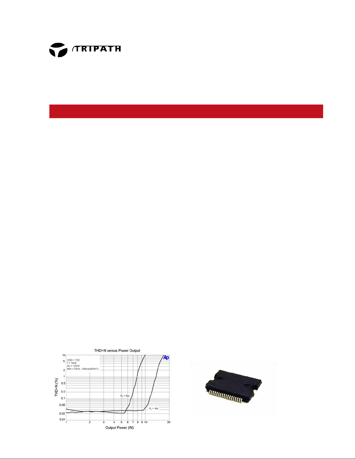
TYPICAL PERFORMANCE
FEATURES
Class-T architecture
Single Supply Operation
“Audiophile” Quality Sound
0.03% THD+N @ 9W, 4Ω
0.10% IHF-IM @ 1W, 4Ω
11W @ 4Ω, 0.1% THD+N
6W @ 8Ω, 0.1% THD+N
High Power
15W @ 4Ω, 10% THD+N
10W @ 8Ω, 10% THD+N
High Efficiency
81% @ 15W, 4Ω
90% @ 10W, 8Ω
Dynamic Range = 98 dB
Mute and Sleep inputs
Enhanced Turn-on & turn-off pop
suppression
Over-current protection
Over-temperature protection
Bridged outputs
36-pin Power SOP package
1 TA2024C –KLi/1.1/09.06
Page 2

Tripath Technology, Inc. - Technical Information
ABSOLUTE MAXIMUM RATINGS
(Note 1)
SYMBOL PARAMETER Value UNITS
V
DD
V5 Input Section Supply Voltage 6.0 V
SLEEP SLEEP Input Voltage -0.3 to 6.0 V
MUTE MUTE Input Voltage -0.3 to V5+0.3 V
T
STORE
T
A
T
J
Supply Voltage 16 V
Storage Temperature Range -40 to 150
Operating Free-air Temperature Range 0 to 70
Junction Temperature 150
°
°
°
C
C
C
Note 1: Absolute Maximum Ratings indicate limits beyond which damage to the device may occur.
Note 2: See Power Dissipation Derating in the Applications Information section.
OPERATING CONDITIONS (Note 4)
SYMBOL PARAMETER MIN. TYP. MAX. UNITS
V
DD
V
IH
V
IL
Supply Voltage 8.5 12 14.0 V
High-level Input Voltage (MUTE, SLEEP) 3.5 V
Low-level Input Voltage (MUTE, SLEEP) 1 V
Note 3: Recommended Operating Conditions indicate conditions for which the device is functional. See
Electrical Characteristics for guaranteed specific performance limits.
THERMAL CHARACTERISTICS
SYMBOL PARAMETER VALUE UNITS
JC
θ
Junction-to-ambient Thermal Resistance (still air) 50
JA
θ
Junction-to-case Thermal Resistance 2.5 °C/W
C/W
°
2 TA2024C –KLi/1.1/09.06
Page 3

Tripath Technology, Inc. - Technical Information
ELECTRICAL CHARACTERISTICS
See Test/Application Circuit. Unless otherwise specified, VDD = 12V, f = 1kHz, Measurement
Bandwidth = 22kHz, R
= 4Ω, TA = 25 °C, Package heat slug soldered to 2.8 square-inch PC pad.
L
SYMBOL PARAMETER CONDITIONS MIN. TYP. MAX. UNITS
P
O
I
DD,MUTE
I
DD, SLEEP
I
q
THD + N Total Harmonic Distortion Plus
Output Power
(Continuous Average/Channel)
THD+N = 0.1% R
R
THD+N = 10% R
R
= 4Ω
L
= 8Ω
L
= 4Ω
L
= 8Ω
L
Mute Supply Current MUTE = VIH 38 mA
Sleep Supply Current SLEEP = VIH 0.25 2 mA
Quiescent Current VIN = 0 V 61 75 mA
PO = 9W/Channel 0.03 %
9
5.5
12
8
11
6
15
10
Noise
IHF-IM IHF Intermodulation Distortion 19kHz, 20kHz, 1:1 (IHF) 0.10 0.5 %
SNR Signal-to-Noise Ratio
A-Weighted, P
= 15W, RL = 4Ω
OUT
CS Channel Separation f = 1 kHz
< f < 20 kHz
20 Hz
PSRR Power Supply Rejection Ratio VDD = 9V to 13.2V
Vripple = 100mVrms, f=1kHz
η
V
OFFSET
VOH High-level output voltage
Power Efficiency
P
= 10W/Channel, RL = 8Ω
OUT
Output Offset Voltage No Load, MUTE = Logic Low 50 150 mV
3.5 V
98 dB
50
85
60
65 75
65
90 %
(FAULT & OVERLOAD)
VOL Low-level output voltage
1 V
(FAULT & OVERLOAD)
e
Output Noise Voltage A-Weighted, input AC grounded 100
OUT
Note: Minimum and maximum limits are guaranteed but may not be 100% tested.
W
W
W
W
dB
dB
dB
dB
µV
3 TA2024C –KLi/1.1/09.06
Page 4
Tripath Technology, Inc. - Technical Information
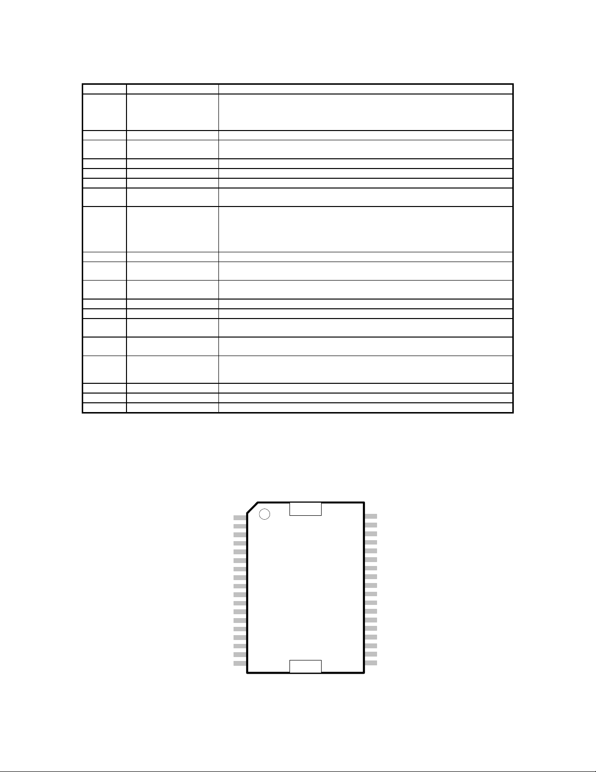
PIN DESCRIPTION
Pin Function Description
2, 3 DCAP2, DCAP1 Charge pump switching pins. DCAP1 (pin 3) is a free running 300kHz square
4, 9 V5D, V5A Digital 5VDC, Analog 5VDC
5, 8,
17
AGND1, AGND2,
AGND3
6 REF Internal reference voltage; approximately 1.0 VDC.
7 OVERLOADB A logic low output indicates the input signal has overloaded the amplifier.
10, 14 OAOUT1, OAOUT2 Input stage output pins.
11, 15 INV1, INV2 Single-ended inputs. Inputs are a “virtual” ground of an inverting opamp with
12 MUTE When set to logic high, both amplifiers are muted and in idle mode. When low
16 BIASCAP Input stage bias voltage (approximately 2.4VDC).
18 SLEEP When set to logic high, device goes into low power mode. If not used, this pin
19 FAULT A logic high output indicates thermal overload, or an output is shorted to ground,
20, 35 PGND2, PGND1 Power Grounds (high current)
22 DGND Digital Ground. Connect to AGND locally (near the TA2024C).
24, 27;
31, 28
25, 26,
29, 30
13, 21,
OUTP2 & OUTM2;
OUTP1 & OUTM1
VDD2, VDD2
VDD1, VDD1
NC Not connected. Not bonded internally.
23, 32,
34
33 VDDA Analog 12VDC
36 CPUMP Charge pump output (nominally 10V above VDDA)
1 5VGEN Regulated 5VDC source used to supply power to the input section (pins 4 and 9).
wave between VDDA and DGND (12Vpp nominal). DCAP2 (pin 2) is level shifted
10 volts above DCAP1 (pin 3) with the same amplitude (12Vpp nominal),
frequency, and phase as DCAP1.
Analog Ground
approximately 2.4VDC bias.
(grounded), both amplifiers are fully operational. If left floating, the device stays in
the mute mode. This pin should be tied to GND if not used. Unlike previous
Tripath devices, the input bias is still active, even if the MUTE pin is tied to a logic
high.
should be grounded
or another output.
Bridged output pairs
Supply pins for high current H-bridges, nominally 12VDC.
TA2024C PINOUT
+5VGEN
DCAP2
DCAP1
V5D
AGND1
REF
OVERLOADB
AGND2
V5A
OAOUT1
INV1
MUTE
NC
OAOUT2
INV2
BIASCAP
AGND3
SLEEP
36-pin Power SOP Package
(Top View)
1
2
3
4
5
6
7
8
9
10
11
12
13
14
15
16
17
18
36
35
34
33
32
31
30
29
28
27
26
25
24
23
22
21
20
19
CPUMP
PGND1
NC
VDDA
NC
OUTP1
VDD1
VDD1
OUTM1
OUTM2
VDD2
VDD2
OUTP2
NC
DGND
NC
PGND2
FAULT
4 TA2024C –KLi/1.1/09.06
Page 5
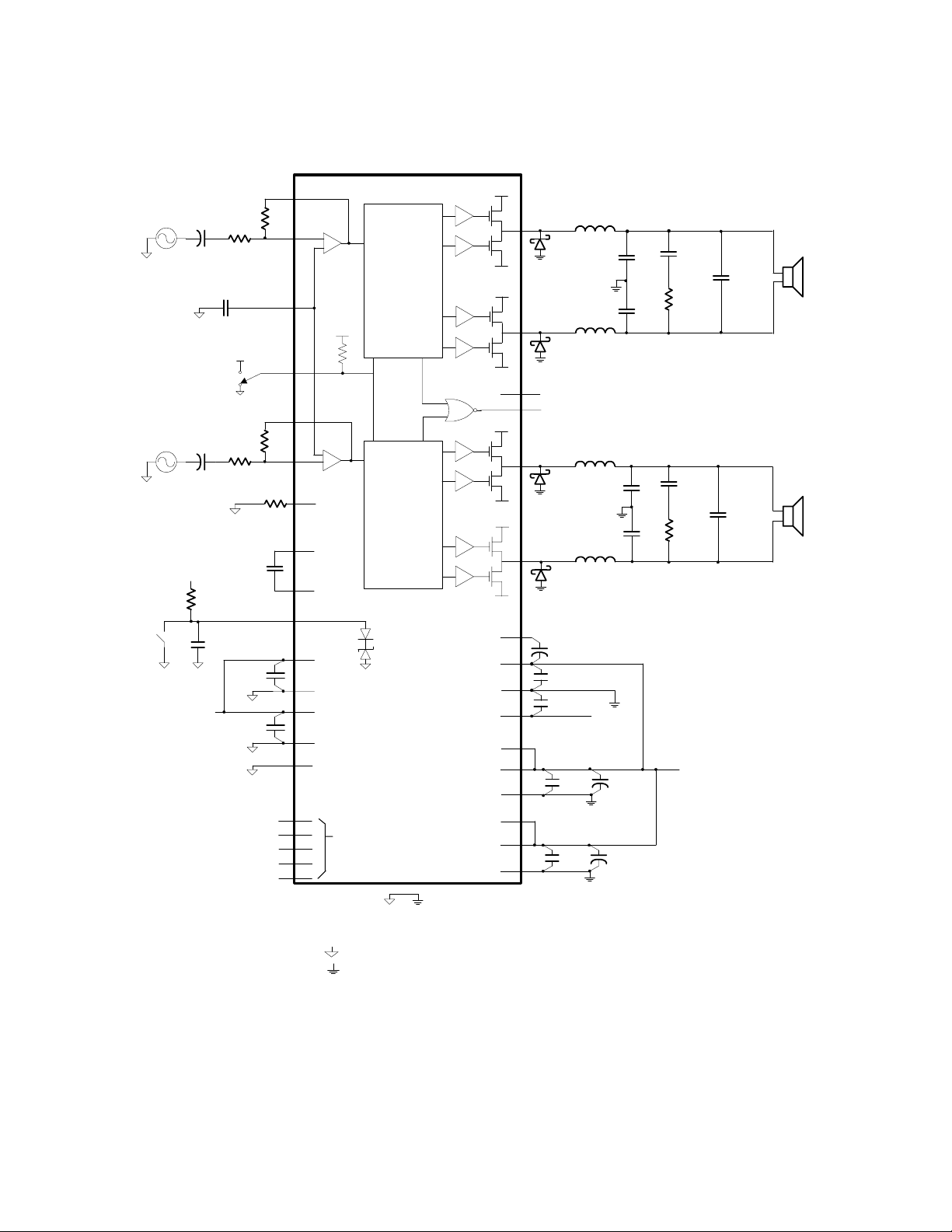
APPLICATION /TEST CIRCUIT
TA2024C
10
OAOUT1
R
F
20KΩ
C
I
2.2uF
(Pin 8)
2.2uF
+12V
To Pin 1
0.1uF
C
I
1MΩ
+
20KΩ
C
A
+
(Pin 8)
0.1uF
R
I
BIASCAP
5V
R
20KΩ
R
I
20KΩ
8.25KΩ, 1%
0.1uF
0.1uF
0.1uF
INV1
MUTE
OAOUT2
F
INV2
R
C
D
C
S
C
S
11
Processing
&
16
Modulation
5V
12
14
15
6
REF
REF
3
DCAP1
2
DCAP2
SLEEP
18
4
V5D
5
AGND1
9
V5A
8
AGND2
17
AGND3
Processing
&
Modulation
5V
13
21
NC
23
32
34
Tripath Technology, Inc. - Technical Information
VDD1
L
o
D
O
D
FAULT
OVERLOADB
D
O
D
(Pin 20)
+
C
1uF
C
S
0.1uF
C
S
0.1uF
C
0.1uF
(Pin 35)
10uH, 2A
O
10uH, 2A
10uH, 2A
O
P
C
SW
0.1uF
SW
10uH, 2A
L
o
L
o
(Pin 20)
L
o
To Pins 4,9
*C
0.47uF
*C
0.47uF
*C
0.47uF
*C
0.47uF
+
C
SW
180uF, 16V
+
C
SW
180uF, 16V
C
Z
o
0.22uF
C
DO
Z
VDD
(+12V)
0.01uF
C
DO
0.01uF
R
Z
o
10Ω, 1/2W
C
o
0.22uF
R
Z
o
10Ω, 1/2W
R
L
4Ω or *8Ω
R
L
4Ω or *8Ω
CPUMP
VDDA
DGND
+5VGEN
VDD1
VDD1
PGND1
VDD2
VDD2
PGND2
PGND1
VDD1
PGND1
19
VDD2
PGND2
VDD2
PGND2
36
22
30
29
35
25
26
20
28
24
27
33
31
1
OUTP1
(Pin 35)
OUTM1
(Pin 35)
7
OUTP2
(Pin 20)
OUTM2
Note: Analog and Digital/Power Grounds must
be connected locally at the TA2024B
Analog Ground
Digital/Power Ground
All Diodes Motorola MBRS130T3
* Use Co = 0.22µF for 8 Ohm loads
5 TA2024C –KLi/1.1/09.06
Page 6
=
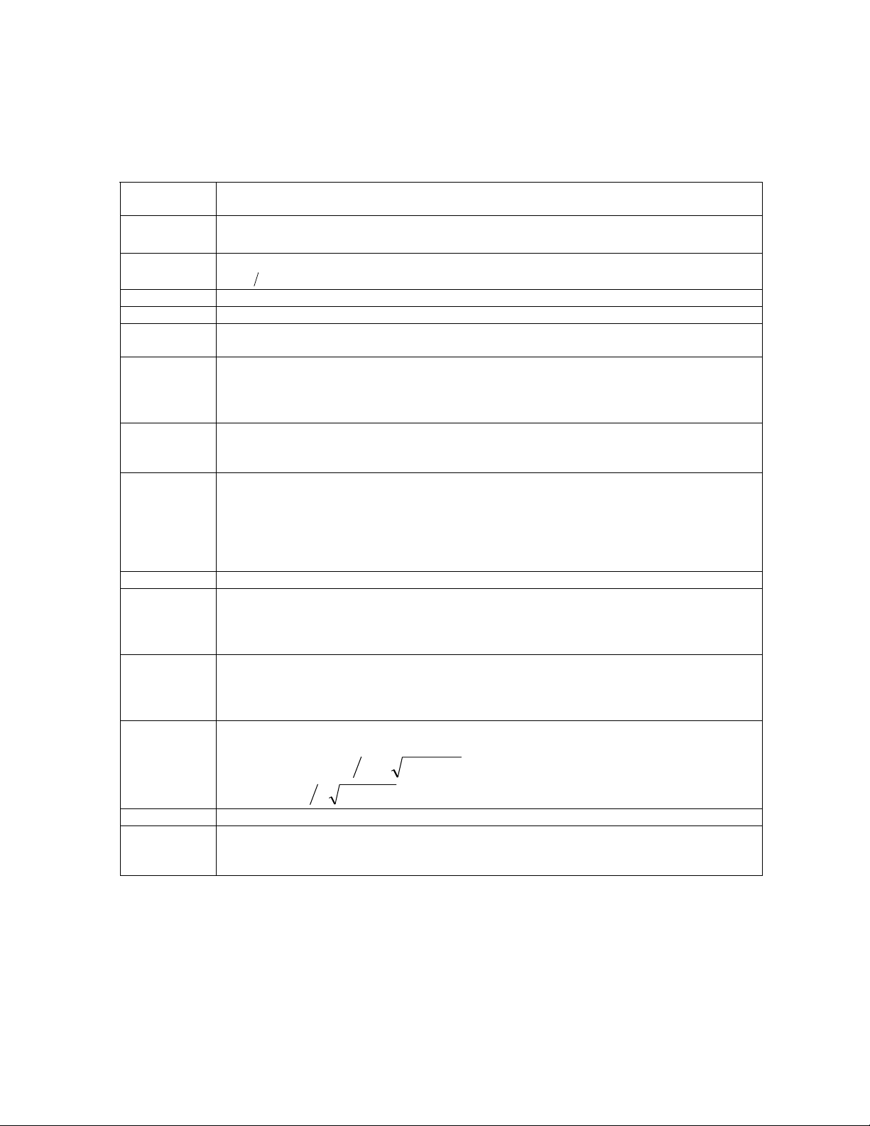
EXTERNAL COMPONENTS DESCRIPTION
Tripath Technology, Inc. - Technical Information
(Refer to the Application/Test Circuit)
Components Description
R
Inverting Input Resistance to provide AC gain in conjunction with RF. This input is
I
biased at the BIASCAP voltage (approximately 2.4VDC).
RF
Feedback resistor to set AC gain in conjunction with R
;
I
. Please refer
)R/R(12A
IFV
to the Amplifier Gain paragraph in the Application Information section.
CI AC input coupling capacitor which, in conjunction with RI, forms a highpass filter at
)CR2(1f
π=
IIC
R
Bias resistor. Locate close to pin 6 (REF) and ground at pin 8 (AGND2).
REF
CA BIASCAP decoupling capacitor. Should be located close to pin 16.
CD Charge pump input capacitor. This capacitor should be connected directly between
pins 2 (DCAP2) and 3 (DCAP1) and located physically close to the TA2024C.
CP Charge pump output capacitor that enables efficient high side gate drive for the
internal H-bridges. To maximize performance, this capacitor should be connected
directly between pin 36 (CPUMP) and pin 33 (VDDA). Please observe the polarity
shown in the Application/ Test Circuit.
CS Supply decoupling for the low current power supply pins. For optimum performance,
these components should be located close to the pin and returned to their
respective ground as shown in the Application/Test Circuit.
CSW Supply decoupling for the high current, high frequency H-Bridge supply pins. These
components must be located as close to the device as possible to minimize supply
overshoot and maximize device reliability. Both the high frequency bypassing
(0.1uF) and bulk capacitor (180uF) should have good high frequency performance
including low ESR and low ESL. Panasonic HFQ or FC capacitors are ideal for the
bulk capacitor.
CZ Zobel Capacitor.
RZ Zobel resistor, which in conjunction with CZ, terminates the output filter at high
frequencies. The combination of R
and CZ minimizes peaking of the output filter
Z
under both no load conditions or with real world loads, including loudspeakers which
usually exhibit a rising impedance with frequency.
DO Schottky diodes that minimize undershoots of the outputs with respect to power
ground during switching transitions. For maximum effectiveness, these diodes must
be located close to the output pins and returned to their respective PGND. Please
see Application/Test Circuit for ground return pin.
LO Output inductor, which in conjunction with CO and CDO, demodulates (filters) the
switching waveform into an audio signal. Forms a second order filter with a cutoff
frequency of
CRQ CL2
=
fπ=
O TOTC
where C
TOTTOTL
O
and a quality factor of
)CL2(1
= CO || 2 * CDO.
TOT
CO Output capacitor.
CDO Differential Output Capacitor. Differential noise decoupling for reduction of
conducted emissions. Must be located near chassis exit point for maximum
effectiveness.
6 TA2024C –KLi/1.1/09.06
Page 7
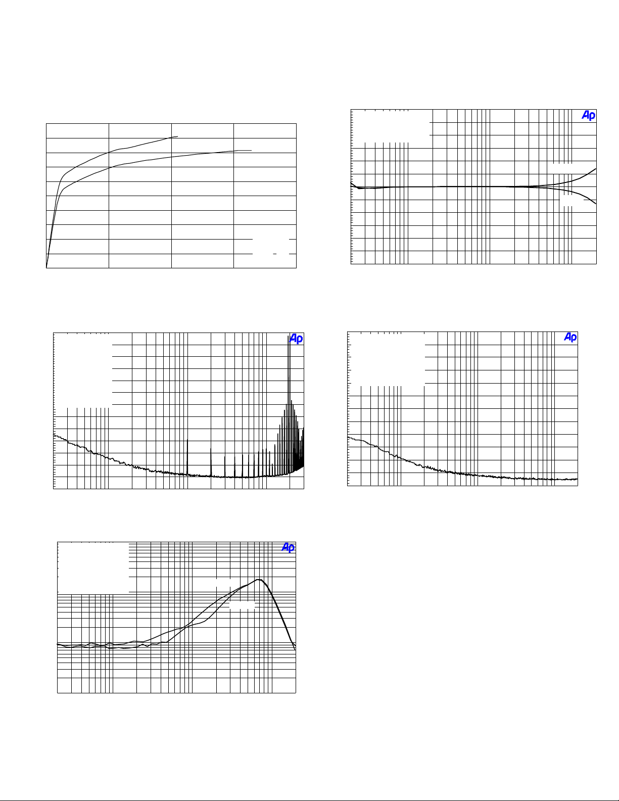
TYPICAL PERFORMANCE
Tripath Technology, Inc. - Technical Information
Efficiency versus Output
100
90
80
RL = 8Ω
70
60
50
40
Efficiency (%)
30
20
10
0
0 5 10 15 20
RL = 4Ω
Power
Output Power (W)
Intermodulation Distortion
+0
-10
19kHz, 20kHz, 1:1
VDD = 12V
-20
Pout = 1W
R
= 4Ω
L
-30
32k FFT
-40
F
= 65kHz
S
f = 1kHz
-50
BW = 22Hz - 80kHz
-60
-70
FFT (dBr)
-80
-90
-100
-110
-120
-130
20 30k50 100 200 500 1k 2k 5k 10k 20k
Frequency (Hz)
1
VDD = 12V
0.5
Po @ 4Ω = 4W
Po @ 8Ω = 2W
BW = 22Hz - 22kHz
0.2
and CZ = 0.22uF for 8Ω
C
O
0.1
0.05
THD+N versus Frequency
RL = 4Ω
RL = 8Ω
VDD = 12V
f = 1kHz
THD+N < 10%
+3
VDD = 12V
+2.5
Pout = 1W
+2
C
and CZ = .22uF for 8Ω
O
+1.5
+1
+0.5
RL = 8Ω
+0
-0.5
RL = 4Ω
-1
-1.5
Output Amplitude (dBr)
-2
-2.5
-3
20 20k50 100 200 500 1k 2k 5k 10k
Frequency (Hz)
Frequency Response
+0
VDD = 12V
-10
R
= 4Ω
L
-20
32k FFT
F
= 65kHz
S
-30
Av = 12V/V
BW = 22Hz - 20kHz(AES17)
-40
-50
-60
-70
-80
Noise FFT (dBV)
-90
-100
-110
-120
20 20k50 100 200 500 1k 2k 5k 10k
Noise Floor
Frequency (W)
0.02
THD+N (%)
0.01
0.005
0.002
0.001
20 20k50 100 200 500 1k 2k 5k 10k
Frequency (Hz)
7 TA2024C –KLi/1.1/09.06
Page 8
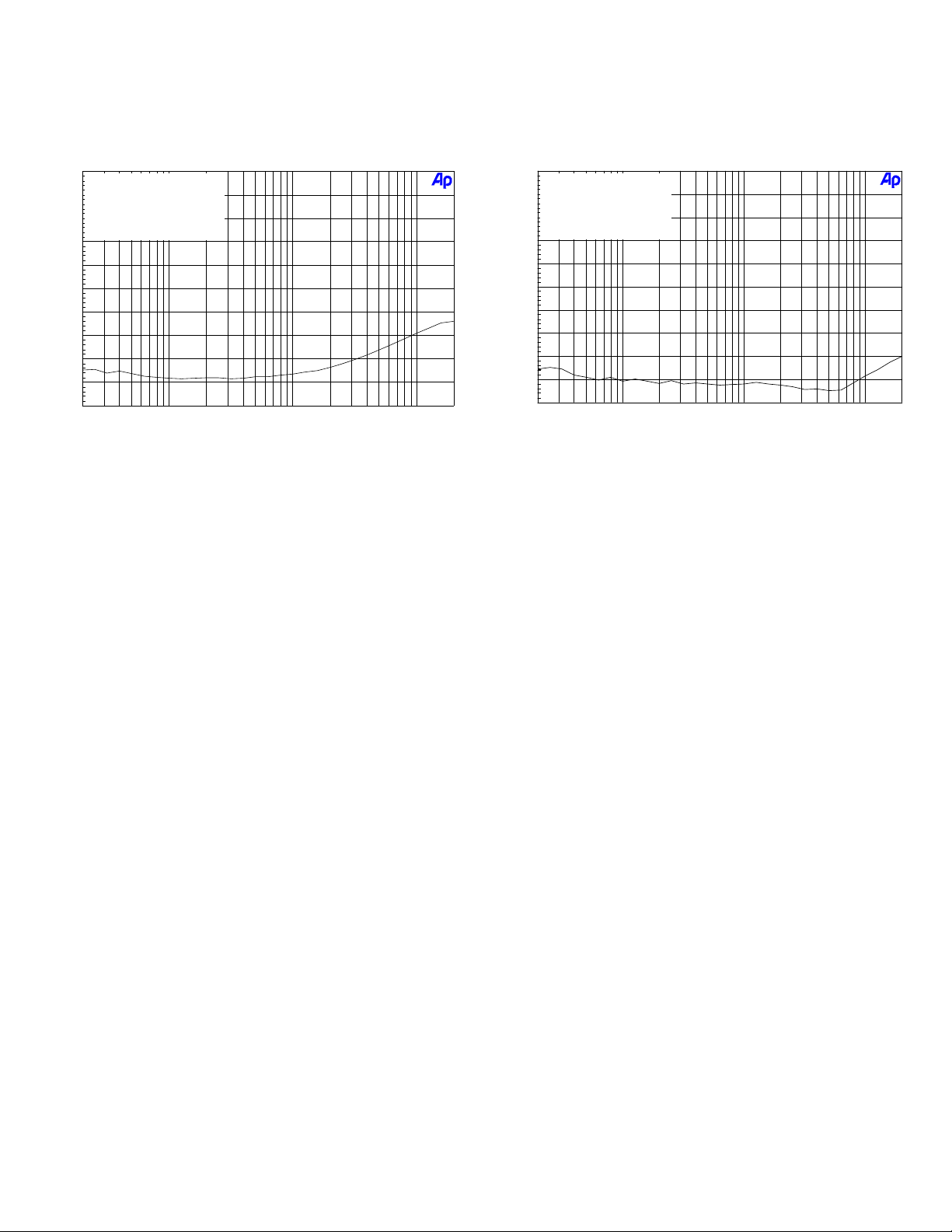
TYPICAL PERFORMANCE
Tripath Technology, Inc. - Technical Information
T T T T T T T T
+0
VDD = 12V
-10
Po = 1W
R
= 4Ω
L
-20
BW = 22Hz - 22kHz
L6, L7, L8, L9 = 8RHB2 Inductors
-30
-40
-50
-60
-70
-80
Channel Separation (dBr)
-90
-100
20 20k50 100 200 500 1k 2k 5k 10k
Channel Separation versus Frequency
Frequency (Hz)
T T T T T T T T
+0
VDD = 12V
-10
Po = 1W
R
= 4Ω
L
-20
BW = 22Hz - 22kHz
L6, L7, L8, L9 = DS86 Inductors
-30
-40
-50
-60
-70
-80
Channel Separation (dBr)
-90
-100
20 20k50 100 200 500 1k 2k 5k 10k
Channel Separation versus Frequency
Frequency (Hz)
8 TA2024C –KLi/1.1/09.06
Page 9
APPLICATION INFORMATION
Layout Recommendations
Tripath Technology, Inc. - Technical Information
The TA2024C is a power (high current) amplifier that operates at relatively high switching
frequencies. The outputs of the amplifier switch between the supply voltage and ground at high
speeds while driving high currents. This high-frequency digital signal is passed through an LC
low-pass filter to recover the amplified audio signal. Since the amplifier must drive the inductive
LC output filter and speaker loads, the amplifier outputs can be pulled above the supply voltage
and below ground by the energy in the output inductance. To avoid subjecting the TA2024C to
potentially damaging voltage stress, it is critical to have a good printed circuit board layout. It is
recommended that Tripath’s layout and application circuit be used for all applications and only be
deviated from after careful analysis of the effects of any changes. Please contact Tripath
Technology for further information regarding reference design material regarding the TA2024C.
Output Stage layout Considerations and Component Selection Criteria
Proper PCB layout and component selection is a major step in designing a reliable TA2024C
power amplifier. The supply pins require proper decoupling with correctly chosen components to
achieve optimal reliability. The output pins need proper protection to keep the outputs from going
below ground.
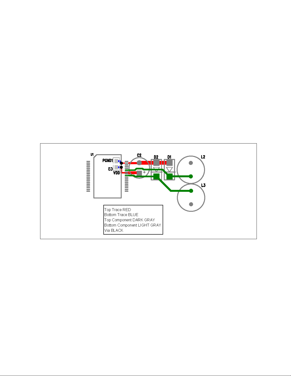
The above layout shows ideal component placement and routing for channel 1 (the same design
criteria applies to channel 2). This shows that C3, a 0.1uF surface mount 0805 capacitor, should
be the first component placed and must decouple VDD1 (pins 29 and 30) directly to PGND1
(pin35). C2, a low ESR, electrolytic capacitor, should also decouple VDD1 directly to PGND1.
Both C2 and C3 may decouple VDD1 to a ground plane, but it is critical that the return path to the
PGND1 pin of the TA2024C, whether it is a ground plane or a trace, be a short and direct low
impedance path. Effectively decoupling VDD will shunt any power supply trace length inductance.
The diodes and inductors shown are for channel 1’s outputs. D1 and L2 connect to the OUTP1
pin and D2 and L3 connect to the OUTM1 pin of the TA2024C. Each output must have a Schottky
or Ultra Fast Recovery diode placed near the TA2024C, preferably immediately after the
decoupling capacitors and use short returns to PGND1. These low side diodes, D1 and D2, will
prevent the outputs from going below ground. To be optimally effective they must have a short
and direct return path to its proper ground pin (PGND1) of the TA2024C. This can be achieved
with a ground plane or a trace.
The output inductors, L2 and L3, should be placed close to the TA2024C without compromising
the locations of the closely placed supply decoupling capacitors and output diodes. The purpose
of placing the output inductors close to the TA2024C output pins is to reduce the trace length of
the switching outputs. This will aid in reducing radiated emissions.
9 TA2024C –KLi/1.1/09.06
Page 10

Tripath Technology, Inc. - Technical Information
Please see the External Component Description section on page 6 for more details on the abovementioned components. The Application/ Test Circuit refers to the low side diodes as D
both supply decoupling capacitors as C
SW
.
, and
O
TA2024C Amplifier Gain
The ideal gain of the TA2024C is set by the ratio of two external resistors, RI and RF, and is given
by the following formula:
V
O
V
I
R
F
−=
12
R
I
where VI is the input signal level and VO is the differential output signal level across the speaker.
Please note that V
is 180° out of phase with VI.
O
The ideal gain of the TA2024C is 12V/V, whereas typical values are: A
11.7V/V for 8
Ω.
= 11.5V/V for 4Ω and
V
Mute Pin
The mute pin must be driven to a logic low or logic high state for proper operation. To enable the
amplifier, connect the mute pin to a logic low. To enable the mute function, connect the mute pin
to a logic high signal. Please note that the mute pin is a 5V CMOS input pin and the mute signal
should be de-bounced to eliminate a possibility of falsely muting.
When in mute, the internal processor bias voltages are still active in the TA2024C. This
minimizes any turn on pop caused by charging the input coupling capacitor. It is recommended
that the mute is held high during power up or power down to eliminate audible transients.
If turn-on and/or turn-off noise is still present with a TA2024C amplifier, the cause may be other
circuitry external to the TA2024C such as an audio processor or preamp. Multiple audio
processors used in LCD TV’s create audible pops as their power supply collapses. If the
TA2024C is still active (mute pin is low), then these audible pops will be amplified and output to
the speakers. To eliminate this problem, simply activate the mute before the power supply
collapses.
Turn-on and Turn-off Noise
The TA20204C has improved mute-off and mute-on click performance as compared to previous
Tripath devices including TA2024 and TA2024B. The main improvement was related to keeping
the input stage biased up during mute, but other specific circuit details, beyond the scope of the
data sheet, were also improved.
But as with the previous devices, many complaints about turn on and off clicks were not actually
caused by the TA2024C. As noted above, a typical cause of turn off pop is related to the audio
processor that provides the audio input to the TA2024C amplifier. The audio processor used for
most LCD TV’s produces a pop when its power supply collapses. Thus, it is recommended that
the TA2024C mute pin is pulled high before the power supply is removed.
The time that it takes to activate mute has been reduced in the TA2024C as opposed to TA2024
and TA2024B. This allows for the mute to be activated before the audio processor power supply
can collapse. Thus, any possibility of a pop being amplified by the TA2024C can be adverted.
The remaining source of click is the residual output offset. This pop would normally be masked if
the TA2024C is playing music but in some cases, may be undesirable due to application
requirements. The level of the pop is proportional to the offset, which has a specified maximum
of 150mV as stated in the Electrical Characteristics Section.
10 TA2024C –KLi/1.1/09.06
Page 11
Tripath Technology, Inc. - Technical Information
In most cases, the pop caused by the output offset is not objectionable. But in those cases that
there is concern about the residual pop, the offset can be nulled. There are several ways to trim
the offset. These include using a trim pot, with current limiting resistor, using an active DC servo
comprised of op-amps, resistors and switches, and finally, a look-up table of resistor values
attached to the input. The last scheme is implemented on the EB-TA2024C. Please refer to the
EB-TA2024C document at www.tripath.com
for additional information on this circuit.
Please note that while a DC servo is automatic, and thus, does not require manual adjustment, it
is not the best solution. This is because the DC servo has to be slow enough so as not to react to
low frequency audio signals. Thus, it is not possible for such a circuit to eliminate a mute off pop
caused by DC offset. The servo is effective for eliminating mute on pops, since the DC offset
would be nulled to zero by the time the TA2024C is muted. A DC servo, in conjunction, with a
relay is an effective method for completely eliminating mute off and mute on pops, but due to the
small residual pop caused by the TA2024C offset, it is unlikely that such a sophisticated scheme
would be implemented for high-volume production designs.
Output Voltage Offset
The DC offset voltages that appear at the speaker terminals of a TA2024C amplifier are typically
small and for most applications no DC offset correction is necessary. The TA2024C is 100%
tested to ensure that the differential output DC offset voltage is less than +/-150mV. However
this DC offset can cause a small turn on and turn off pop, depending on the offset value for that
specific IC. Every TA2024C IC will have a different offset voltage for each channel.
If the output offset is deemed unacceptable from a turn on/off pop standpoint, there are three
recommended methods for correcting it. These methods of trimming the offset voltage are
optional and for most cases the additional circuitry is not needed.
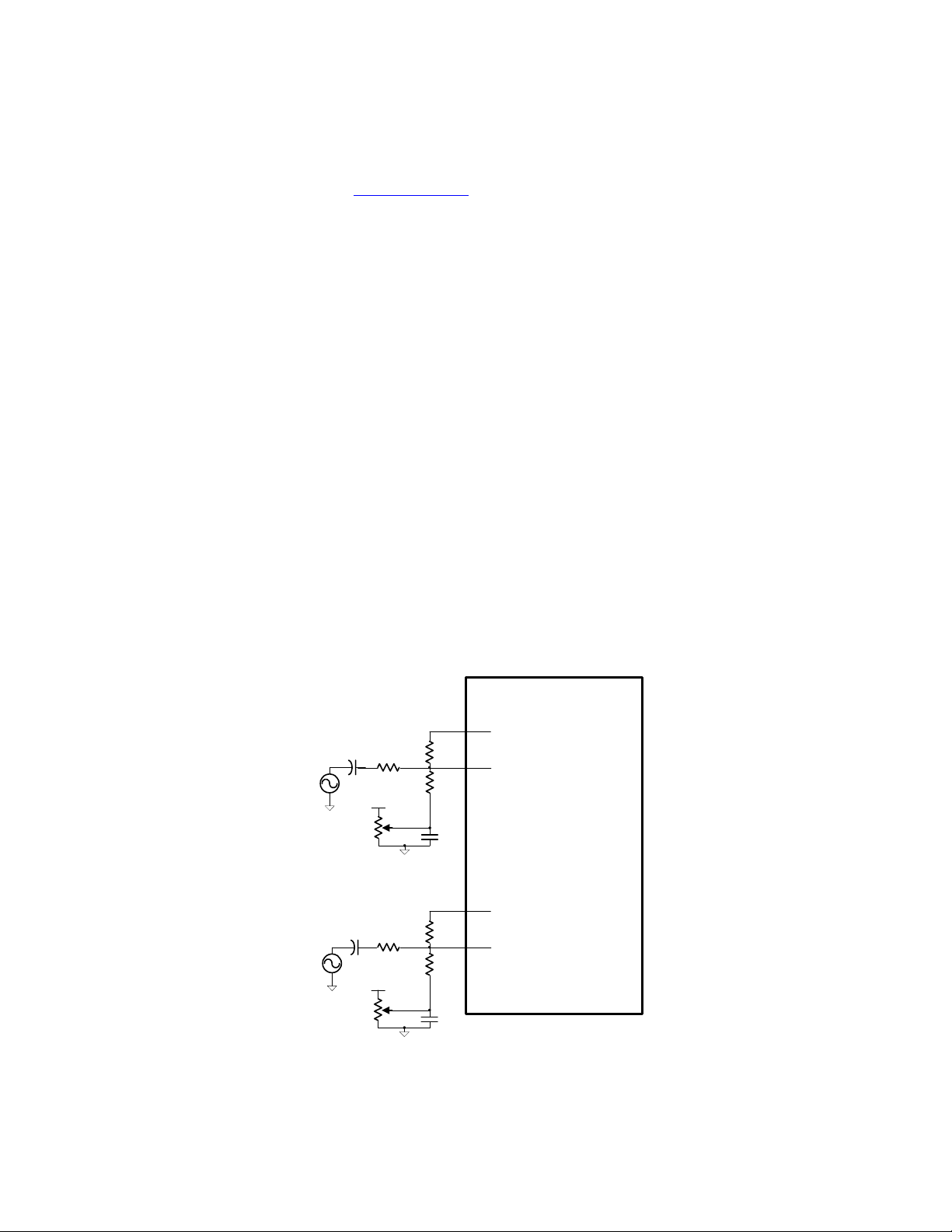
1) A potentiometer can be used at the input of the TA2024C as shown in the figure below. By
changing the input bias voltage the output DC offset voltage can be trimmed. Two separate
potentiometers must be used to trim both channels.
C
I
2.2uF
+
V5A (pin 28)
R
10KΩ
Offset Trim
Potentiometer
C
I
2.2uF
+
V5A (pin 28)
R
10KΩ
Offset Trim
Potentiometer
29
OAOUT1
R
F
R
20KΩ
I
20KΩ
OFA
R
F
R
I
20KΩ
20KΩ
OFA
INV1
R
OFB
1MΩ
C
OF
0.1uF
OAOUT2
INV2
R
OFB
1MΩ
C
OF
0.1uF
30
TA2024C
1
2
11 TA2024C –KLi/1.1/09.06
Page 12
Tripath Technology, Inc. - Technical Information
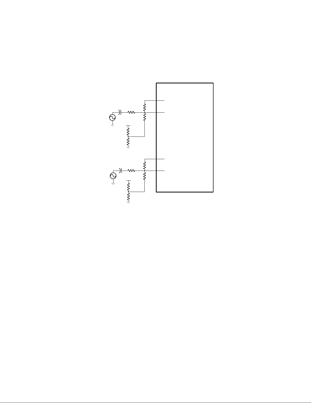
2) In cases where manually trimming potentiometers is not possible, resistors can be used in
place of potentiometers. Since each TA2024C has different offset voltage, the output offset
voltage will need to be measured for both channel 1 and channel 2 and then resistors will
have to be added on the PC board to trim the offset. Below is a lookup table for resistor
values for corresponding offset voltages. Both Rx and Ry values should be 1% tolerance
resistors. Please refer to the EB-TA2024C document for more information on this manual
trim method using resistors.
29
OAOUT1
R
I
20KΩ
R
F
20KΩ
R
X1
R
Y1
R
1MΩ
OFB
INV1
30
TAA2024C
C
I
2.2uF
+
V5A (pin 28)
OAOUT2
R
1MΩ
OFB
INV2
1
2
C
I
2.2uF
+
V5A (pin 28)
R
I
20KΩ
R
F
20KΩ
R
X2
R
Y2
12 TA2024C –KLi/1.1/09.06
Page 13

Tripath Technology, Inc. - Technical Information
OFFSET Ry Rx (1%)
150mV
140mV
130mV
120mV
110mV
100mV
90mV
80mV
70mV
60mV
50mV
40mV
30mV
20mV
10mV
0mV
-10mV
-20mV
-30mV
-40mV
-50mV
-60mV
-70mV
-80mV
-90mV
-100mV
-110mV
-120mV
-130mV
-140mV
-150mV
20kΩ 13.3kΩ
20kΩ 13.7kΩ
20kΩ 14.3kΩ
14.7kΩ
20k
Ω
15.4kΩ
20k
Ω
20kΩ 15.8kΩ
20kΩ 16.2kΩ
20kΩ 16.9kΩ
17.4kΩ
20k
Ω
17.8kΩ
20k
Ω
20kΩ 18.7kΩ
20kΩ 19.1kΩ
20kΩ 19.6kΩ
20kΩ 20.5kΩ
20kΩ 21kΩ
21.5kΩ
20k
Ω
22.6kΩ
20k
Ω
23.2kΩ
20k
Ω
20kΩ 24.3kΩ
20kΩ 24.9kΩ
20kΩ 25.5kΩ
26.7kΩ
20k
Ω
27.4kΩ
20k
Ω
20kΩ 28.0kΩ
20kΩ 29.4kΩ
20kΩ 30.1kΩ
20kΩ 31.6kΩ
20kΩ 32.4kΩ
20kΩ 33.2kΩ
34.8kΩ
20k
Ω
35.7kΩ
20k
Ω
3) A DC servo using a dual op amp can also be used to automatically null any offset voltage.
This DC servo will only eliminate the turn off pop since the RC time constant of the DC servo
is very slow. Please contact Tripath sales for additional information on the DC servo circuit.
Protection Circuits
The TA2024C is guarded against over-temperature and over-current conditions. When the
device goes into an over-temperature or over-current state, the FAULT pin goes to a logic HIGH
state indicating a fault condition. When this occurs, the amplifier is muted, all outputs are TRISTATED, and will float to 1/2 of V
DD
.
Over-temperature Protection
An over-temperature fault occurs if the junction temperature of the part exceeds approximately
155
°C. The thermal hysteresis of the part is approximately 45°C, therefore the fault will
automatically clear when the junction temperature drops below 110
°C.
13 TA2024C –KLi/1.1/09.06
Page 14

Over-current Protection
Tripath Technology, Inc. - Technical Information
An over-current fault occurs if more than approximately 7 amps of current flows from any of the
amplifier output pins. This can occur if the speaker wires are shorted together or if one side of
the speaker is shorted to ground. An over-current fault sets an internal latch that can only be
cleared if the MUTE pin is toggled or if the part is powered down. Alternately, if the MUTE pin is
connected to the FAULT pin, the HIGH output of the FAULT pin will toggle the MUTE pin and
automatically reset the fault condition.
Overload
The OVERLOADB pin is a 5V logic output. When low, it indicates that the level of the input signal
has overloaded the amplifier resulting in increased distortion at the output. The OVERLOADB
signal can be used to control a distortion indicator light or LED through a simple buffer circuit, as
the OVERLOADB cannot drive an LED directly.
Sleep Pin
The SLEEP pin is a 5V logic input that when pulled high (>3.5V) puts the part into a low quiescent
current mode. This pin is internally clamped by a zener diode to approximately 6V thus allowing
the pin to be pulled up through a large valued resistor (1meg
Ω recommended) to V
. To disable
DD
SLEEP mode, the sleep pin should be grounded.
Fault Pin
The FAULT pin is a 5V logic output that indicates various fault conditions within the device.
These conditions include: low supply voltage, low charge pump voltage, low 5V regulator voltage,
over current at any output, and junction temperature greater than approximately 155
°C. All faults
except overcurrent all reset upon removal of the condition. The FAULT output is capable of
directly driving an LED through a series 2k
Ω resistor. If the FAULT pin is connected directly to
the MUTE input an automatic reset will occur in the event of an over-current condition.
Power Dissipation Derating
For operating at ambient temperatures above 25
150
°C maximum junction temperature, TJMAX as given by the following equation:
°C the device must be derated based on a
)TT(
−
P
DISS
=
AJMAX
θ
JA
where…
= maximum power dissipation
P
DISS
= maximum junction temperature of TA2024C
T
JMAX
= operating ambient temperature
T
A
θ
= junction-to-ambient thermal resistance
JA
14 TA2024C –KLi/1.1/09.06
Page 15
Tripath Technology, Inc. - Technical Information
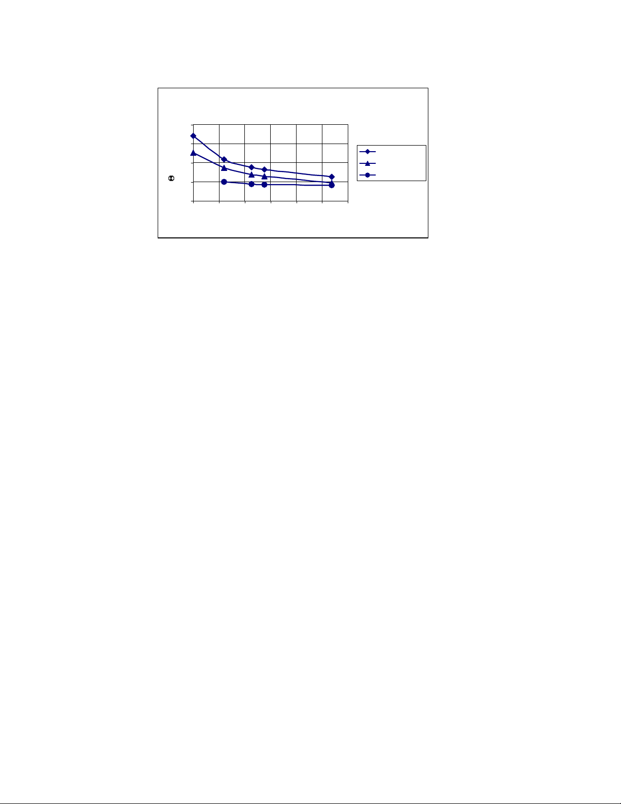
Where θJA of the package is determined from the following graph:
vs Copper Area
Θ
JA
50
40
C/W)
o
30
(
JA
20
10
0123456
Copper Area (square inches)
Pdiss - 1.35W
Pdiss - 2W
Pdiss - 3.4W
In the above graph, Copper Area is the size of the copper pad on the PC board to which the heat
slug of the TA2024C is soldered.
The heat slug must be soldered to the PC Board to increase
the maximum power dissipation capability of the TA2024C package. Soldering will minimize the
likelihood of an over-temperature fault occurring during continuous heavy load conditions. The
vias used for connecting the heatslug to the copper area on the PCB should be 0.013” diameter.
Performance Measurements of the TA2024C
The TA2024C operates by generating a high frequency switching signal based on the audio input.
This signal is sent through a low-pass filter (external to the Tripath amplifier) that recovers an
amplified version of the audio input. The frequency of the switching pattern is spread spectrum
and typically varies between 100kHz and 1.0MHz, which is well above the 20Hz – 20kHz audio
band. The pattern itself does not alter or distort the audio input signal but it does introduce some
inaudible components.
The measurements of certain performance parameters, particularly noise related specifications
such as THD+N, are significantly affected by the design of the low-pass filter used on the output
as well as the bandwidth setting of the measurement instrument used. Unless the filter has a
very sharp roll-off just beyond the audio band or the bandwidth of the measurement instrument is
limited, some of the inaudible noise components introduced by the Tripath amplifiers switching
pattern will degrade the measurement.
One feature of the TA2024C is that it does not require large multi-pole filters to achieve excellent
performance in listening tests, usually a more critical factor than performance measurements.
Though using a multi-pole filter may remove high-frequency noise and improve THD+N type
measurements (when they are made with wide-bandwidth measuring equipment), these same
filters degrade frequency response. The TA2024C Evaluation Board uses the Test/Application
Circuit in this data sheet, which has a simple two-pole output filter and excellent performance in
listening tests. Measurements in this data sheet were taken using this same circuit with a limited
bandwidth setting in the measurement instrument.
15 TA2024C –KLi/1.1/09.06
Page 16
PACKAGE INFORMATION
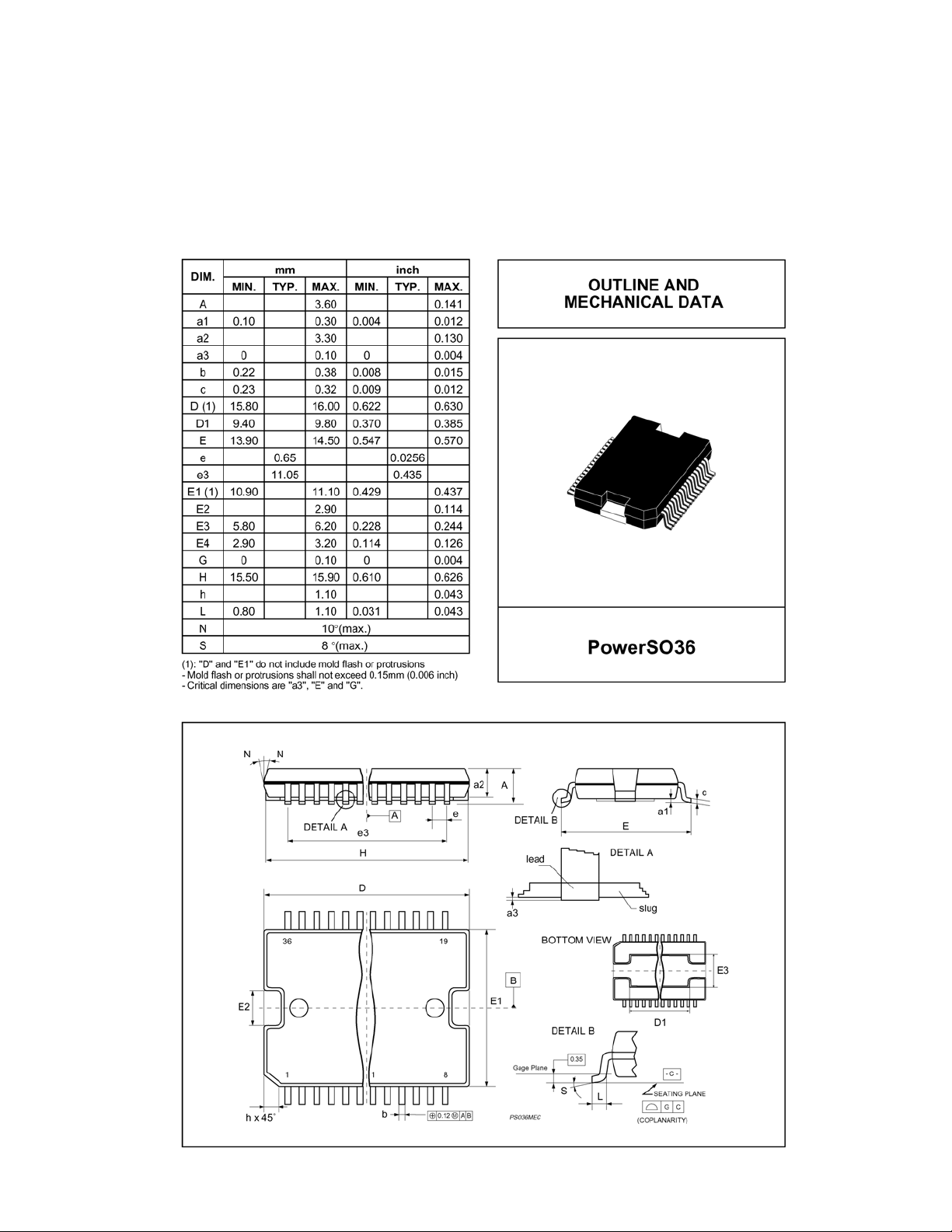
The package for the TA2024C is a 36-Lead Power Small Outline Package (PSOP), similar to
JEDEC outline MO-166, variation AE. Tripath currently has two suppliers for this package. We
recommend that the exposed copper heatslug width for the PCB design be at least 7.3mm wide
to accommodate the heatslug width variation for each package. Package dimensions are based
on millimeters. Measurements in inches are provided as reference only.
Tripath Technology, Inc. - Technical Information
16 TA2024C –KLi/1.1/09.06
Page 17
Tripath Technology, Inc. - Technical Information
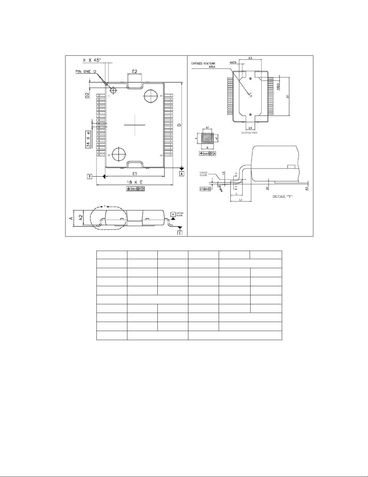
Outline and mechanical data for PSOP36
DIM MIN MAX DIM MIN MAX
A - 3.600 E1 11.00 BSC
A1 0.100 - E2 - 2.900
A2 3.000 3.300 E3 6.300 7.300
A3 0.025 0.152 E4 2.700 2.900
D 15.90 BSC E5 - 1.000
D1 9.000 13.000 L 0.800 1.100
D2 - 1.100 L1 1.60 REF
D3 - 1.000 L2 0.350 BSC
E 14.200 BSC All DIM measured in mm
17 TA2024C –KLi/1.1/09.06
Page 18

Tripath Technology, Inc. - Technical Information
PRELIMINARY INFORMATION – The above specification is for a device that is currently in development.
All specifications and device descriptions are subject to change based on product analysis and
characterization. Please contact Tripath Technology for additional information not included or covered in
this preliminary document.
Tripath Technology Inc. reserves the right to make changes without further notice to any products herein
to improve reliability, function or design. Tripath does not assume any liability arising out of the application
or use of any product or circuit described herein; neither does it convey any license under its patent
rights, nor the rights of others.
Tripath and Digital Power Processing are trademarks of Tripath Technology Inc. Other trademarks
referenced in this document are owned by their respective companies
.
TRIPATH’S PRODUCTS ARE NOT AUTHORIZED FOR USE AS CRITICAL COMPONENTS IN LIFE
SUPPORT DEVICES OR SYSTEMS WITHOUT THE EXPRESS WRITTEN CONSENT OF THE
PRESIDENT OF TRIPATH TECHNOLOGY INC.
As used herein:
1. Life support devices or systems are devices or systems which, (a) are intended for surgical
implant into the body, or (b) support or sustain life, and whose failure to perform, when properly used in
accordance with instructions for use provided in this labeling, can be reasonably expected to result in
significant injury to the user.
2. A critical component is any component of a life support device or system whose failure to perform
can be reasonably expected to cause the failure of the life support device or system, or to affect its safety
or effectiveness.
Contact Information
TRIPATH TECHNOLOGY, INC
2560 Orchard Parkway, San Jose, CA 95131
408.750.3000 - P
408.750.3001 - F
For more Sales Information, please visit us @ www.tripath.com/cont_s.htm
For more Technical Information, please visit us @ www.tripath.com/data.htm
18 TA2024C –KLi/1.1/09.06
 Loading...