

Page 1
TECHNICAL INFORMATION
Stereo 90W (4
Digital Power Processing
ADVANCED INFORMATION - December 2000
ΩΩΩΩ
) Class-T Digital Audio Amplifier using
TM
Technology TA2022
General Description
The TA2022 is an 90W continuous average, per channel, Class-T Digital Audio Power
Amplifier IC using Tripath’s proprietary Digital Power Processing
amplifiers offer both the audio fidelity of Class-AB and the power efficiency of Class-D
amplifiers.
Applications
!"DVD Players
!"Mini/Micro Component Systems
!"Home Theater
!"Powered Speakers
Benefits
!"Fully integrated solution with internal
FETs
!"Dramatically improves efficiency versus
Class-AB
!"Signal fidelity equal to high quality linear
amplifiers
!"High dynamic range compatible with
digital media such as CD, DVD, and
internet audio
Features
!"Class-T architecture
!"High Power
!"100W @ 4Ω, 1.0% THD+N
!"90W @ 4Ω, 0.1% THD+N
!"60W @ 8Ω, 0.1% THD+N
!"“Audiophile” Quality Sound
!"0.015% THD+N @ 70W 4Ω
!"0.015% THD+N @ 45W 8Ω
!"0.10% IHF-IM @ 25W 4Ω
!"High Efficiency
!"92% @ 88W 8Ω
!"87% @ 125W 4Ω
!"Dynamic Range = 102 dB
!"Mute Input
!"Over-current protection
!"Over and under-voltage protection
!"Single ended outputs
!"Outputs can be operated in bridged mode
!"32-pin SSIP package
TM
technology. Class-T
1 of 29 TA2022, Rev. 0.90, 12.00
Page 2

TECHNICAL INFORMATION
Absolute Maximum Ratings
SYMBOL PARAMETER Value UNITS
VPP, VNN Supply Voltage (VPP1, VPP2, VNN1, VNN2) +/-40 V
V5 Positive 5V Bias Supply
VN10 Voltage for low-side FET drive VNN + 13 V
T
STORE
T
A
T
J
ESDHB ESD Susceptibility – Human Body Model (Note 3)
ESDMM ESD Susceptibility – Machine Model (Note 4)
Voltage at Input Pins (pins 18, 19, 23, 24, 26, 28, 29, 30, 31, 32)
Storage Temperature Range
Operating Free-air Temperature Range (Note 2)
Junction Temperature
All pins (except pin 27)
Pin 27
All pins
Note 1: Absolute Maximum Ratings indicate limits beyond which damage to the device may occur.
See the table below for Operating Conditions.
Note 2: This is a target specification. Characterization is still needed to validate this temperature range.
Note 3: Human body model, 100pF discharged through a 1.5KΩ resistor.
Note 4: Machine model, 220pF – 240pF discharged through all pins.
Operating Conditions
SYMBOL PARAMETER MIN. TYP. MAX. UNITS
VPP, VNN Supply Voltage (VPP1, VPP2, VNN1, VNN2) +/-12 +/-31 +/-36 V
V5
VN10
Positive 5V Bias Supply 4.5 5 5.5 V
Voltage for low side FET drive (Volts above VNN) 9 11 12 V
Note 5: Recommended Operating Conditions indicate conditions for which the device is functional.
See Electrical Characteristics for guaranteed specific performance limits.
Thermal Characteristics
SYMBOL PARAMETER Value UNITS
θ
JC
θ
JA
Junction-to-case Thermal Resistance
Junction-to-ambient Thermal Resistance (still air)
(Note 5)
(Note 1)
-55
-40
6
to 150°
°
to 85°
°
150
°
4000
1500
200
-0.3V to (V5 +0.3V)
V
V
C
C
C
V
V
V
1.0
20
°
°
C/W
C/W
2 of 27 TA2022, Rev. 0.90, 12.00
Page 3

TECHNICAL INFORMATION
Electrical Characteristics
(Notes 6, 7)
TA = 25 °C. See Application/Test Circuit on page 7. Unless otherwise noted, the supply voltage is
VPP=|VNN|=31V.
SYMBOL PARAMETER CONDITIONS MIN. TYP. MAX. UNITS
I
q
I
MUTE
VIH High-level input voltage (MUTE) 3.5 V
VIL Low-level input voltage (MUTE) 1.0 V
VOH High-level output voltage (HMUTE) I
VOL Low-level output voltage (HMUTE) I
V
OFFSET
IOC Over Current Sense Threshold TBD TBD TBD A
I
VPPSENSE
V
VPPSENSE
I
VNNSENSE
V
VNNSENSE
Quiescent Current
(No load, Mute = 0V)
Mute Supply Current
(No load, Mute = 5V)
Output Offset Voltage No Load, MUTE = Logic low
VPPSENSE Threshold Currents Over-voltage turn on (muted)
Threshold Voltages with
R
VPPSENSE
(Note 11)
VNNSENSE Threshold Currents Over-voltage turn on (muted)
Threshold Voltages with
R
VNNSENSE
(Note 11)
= 249KΩ
= 249KΩ
VPP = +31V
VNN = -31V (Note 8)
V5 = 5V (Note 9)
VN10 = 11V (Note 10)
VPP = +31V
VNN = -31V (Note 8)
V5 = 5V (Note 9)
= 3mA 3.5 V
OH
= 3mA 1.0 V
OL
0.1% R
Over-voltage turn off (mute off)
Under-voltage turn off (mute off)
Under-voltage turn on (muted)
Over-voltage turn on (muted)
Over-voltage turn off (mute off)
Under-voltage turn off (mute off)
Under-voltage turn on (muted)
Over-voltage turn off (mute off)
Under-voltage turn off (mute off)
Under-voltage turn on (muted)
Over-voltage turn on (muted)
Over-voltage turn off (mute off)
Under-voltage turn off (mute off)
Under-voltage turn on (muted)
FBA
, R
FBB
, R
resistors
FBC
20
55
45
65
0.5
2
20
-750 750 mV
62
65
162
154
79
72
42.8
40.9
22.2
20.4
174
169
86
77
-42.1
-40.8
-20.2
-17.9
138
36.5
17.8
152
-36.2
-14.8
60
80
25
178
87
47.3
24.4
191
95
-46.8
-22.6
mA
mA
mA
mA
mA
mA
mA
A
µ
A
µ
A
µ
A
µ
V
V
V
V
A
µ
A
µ
A
µ
A
µ
V
V
V
V
TA2022, Rev. 0.90, 12.00 3 of 27
Page 4

TECHNICAL INFORMATION
Performance Characteristics – Single Ended
(Notes 6, 7)
TA = 25 °C. Unless otherwise noted, the supply voltage is VPP=|VNN|=31V, the input frequency is
1kHz and the measurement bandwidth is 20kHz. See Application/Test Circuit on page 7.
SYMBOL PARAMETER CONDITIONS MIN. TYP. MAX. UNITS
P
OUT
THD + N Total Harmonic Distortion Plus
IHF-IM IHF Intermodulation Distortion
SNR Signal-to-Noise Ratio A-Weighted
CS Channel Separation
AV Amplifier Gain
A
VERROR
η
I
SLOAD
e
NOUT
Output Power
(Continuous Average/Channel)
(Note 12)
Noise
Channel to Channel Gain Error
Power Efficiency
Source Current
Output Noise Voltage A-W eighted, input AC grounded 150
VPP = |VNN| = +/-31V, R
THD+N = 0.1%
THD+N = 1.0%
THD+N = 10%
VPP = |VNN| = +/-35V, R
THD+N = 0.1%
THD+N = 10%
= 70W/Channel, RL = 4Ω
P
OUT
VPP = |VNN| = +/-31V
= 45W/Channel, RL = 8Ω
P
OUT
VPP = |VNN| = +/-35V
19kHz, 20kHz, 1:1 (IHF), R
= 25W/Channel
P
OUT
0dB = 90W/Channel, R
0dB = 25W, R
P
OUT
See Application / Test Circuit
P
OUT
See Application / Test Circuit
P
OUT
P
OUT
P
OUT
VPP = +31V
VNN = -31V
V5 = 5V
= 4Ω,
L
= 10W/Channel, RL = 4Ω,
= 10W/Channel, RL = 4Ω
= 88W/Channel, RL = 8
= 125W/Channel, RL = 4Ω
= 125W/Channel, RL = 4
L
L
= 4Ω
L
Performance Characteristics – Bridged Tied Load
TA = 25 °C. Unless otherwise noted, the supply voltage is VPP=|VNN|=30V, the input frequency is
1kHz and the measurement bandwidth is 20kHz.
SYMBOL PARAMETER CONDITIONS MIN. TYP. MAX. UNITS
P
OUT
THD + N Total Harmonic Distortion Plus
IHF-IM IHF Intermodulation Distortion
η
SNR Signal-to-Noise Ratio
e
NOUT
Output Power
(Continuous Average)
(Note 12)
Noise
Power Efficiency
Output Noise Voltage A-W eighted, input AC grounded 220
VPP = |VNN| = +/-30V, R
THD+N = 0.1%
THD+N = 10%
= 100W, RL = 8Ω
P
OUT
19kHz, 20kHz, 1:1 (IHF), R
= 25W
P
OUT
= 225W, RL = 8Ω
P
OUT
A-Weighted, R
0dB = 150W
L
= 8
Ω
L
= 4Ω
= 8Ω
= 4Ω
L
Ω
Ω
(Notes 6, 7)
= 8Ω
= 8Ω
L
80
90
100
125
0.015
0.1 %
102 dB
83 dB
18.1 V/V
0.5 dB
92
60
88
0.015
87
4.59
4.61
45
%
0.05 %
0.10 %
87 %
104 dB
150
235
W
W
W
W
%
%
%
A
A
mA
V
µ
W
W
V
µ
4 of 27 TA2022, Rev. 0.90, 12.00
Page 5

TECHNICAL INFORMATION
Note 6: Minimum and maximum limits are guaranteed but may not be 100% tested.
Note 7: For operation in ambient temperatures greater than 25°C, the device must be derated based on the
maximum junction temperature and the thermal resistance determined by the mounting technique.
Note 8: This specification includes the current draw from the internal buck regulator.
Note 9: This specification includes the current draw from both the TA2022 and the external feedback biasing.
Note 10: This is the current draw of the VN10 pin if an external “floating” 11V supply is used instead of the
internal buck regulator. If an external floating supply is used, the idle current draw of the VNN supply
will be approximately 20mA.
Note 11: These supply voltages are calculated using the IVPPSENSE AND IVNNSENSE values shown in the
Electrical Characteristics table. The typical voltage values shown are calculated using a
RVPPSENSE and RVNNSENSE value of 249kohm without any tolerance variation. The minimum
and maximum voltage limits shown include either a +1% or –1% (+1% for Over-voltage turn on and
Under-voltage turn off, -1% for Over-voltage turn off and Under-voltage turn on) variation of
RVPPSENSE or RVNNSENSE off the nominal 249kohm value. These voltage specifications are
examples to show both typical and worst case voltage ranges for a given RVPPSENSE and
RVNNSENSE resistor value of 249kohm. Please refer to the Application Information section for a
more detailed description of how to calculate the over and under voltage trip voltages for a given
resistor value.
Note 12: The supply voltage limitation for 4 ohm single ended (+/-31V), or 8 ohm bridged (+/-30V), is based on
the current limit protection circuitry. The current limit circuitry may be activated during large output
excursions if the recommended supply voltage ranges are exceeded. This will result in the amplifier
being muted.
TA2022, Rev. 0.90, 12.00 5 of 27
Page 6
TECHNICAL INFORMATION
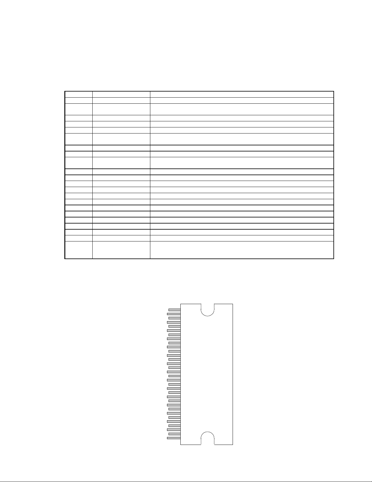
Pin Description
Pin
Function
1, 13 VBOOT2, VBOOT1 Bootstrap voltages for gate drive of high side MOSFET’s
2 VN10 “Floating” supply input. Normally connected to the output of onboard VN10 buck
3 VN10GND Power ground for onboard VN10 generator. Electrically tied to the TA2022 case.
4, 12 VPP2, VPP1 Positive power supply input pins.
5 VN10SW Switching output voltage for onboard VN10 generator (buck converter).
6 NC Not connected internally. May be connected to pin 7 without any loss of
7,10 OUT2, OUT1 Power amplifier outputs.
8, 9 VNN2, VNN1 Negative power supply inputs.
11 NC Not connected internally. May be connected to pin 10 without any loss of
14 VN10FDBK Feedback for onboard VN10 generator (nominally 11V above VNN)
15, 20 AGND Analog Ground.
16, 21 V5 5V power supply input.
17 REF Used to set internal bias. Typically 1.1V
18 VNNSENSE Negative supply voltage sense input.
19 VPPSENSE Positive supply voltage sense input.
22, 25 OAOUT1, OAOUT2 Outputs of Input Stage op amps.
23, 26 INV1, INV2 Inverting inputs of Input Stage op amps.
24 MUTE Logic input. A logic high puts the amplifier in mute mode. Ground if not used.
27 BIASCAP Bandgap reference times two (typically 2.5VDC).
28, 29 FBKGND2, FBKOUT2 Output voltage differential feedback for channel 2.
30,31 FBKGND1, FBKOUT1 Output voltage differential feedback for channel 1.
32 HMUTE Logic Output. A logic high indicates both amplifiers are muted, due to the mute
Description
converter. This voltage must be stable and referenced to VNN.
functionality or performance.
functionality or performance.
pin state, or a “fault” such as an overcurrent, undervoltage, or overvoltage
condition.
32-pin SSIP Package
(Front View)
VBOOT2
VN10
VN10GND
VPP2
VN10SW
OUT2
VNN2
VNN1
OUT1
VPP1
VBOOT1
VN10FDBK
AGND
REF
VNNSENSE
VPPSENSE
AGND
OAOUT1
INV1
MUTE
OAOUT2
INV2
BIASCAP
FBKGND2
FBKOUT2
FBKGND1
FBKOUT1
HMUTE
NC
NC
V5
V5
1
2
3
4
5
6
7
8
9
10
11
12
13
14
15
16
17
18
19
20
21
22
23
24
25
26
27
28
29
30
31
32
6 of 27 TA2022, Rev. 0.90, 12.00
Page 7
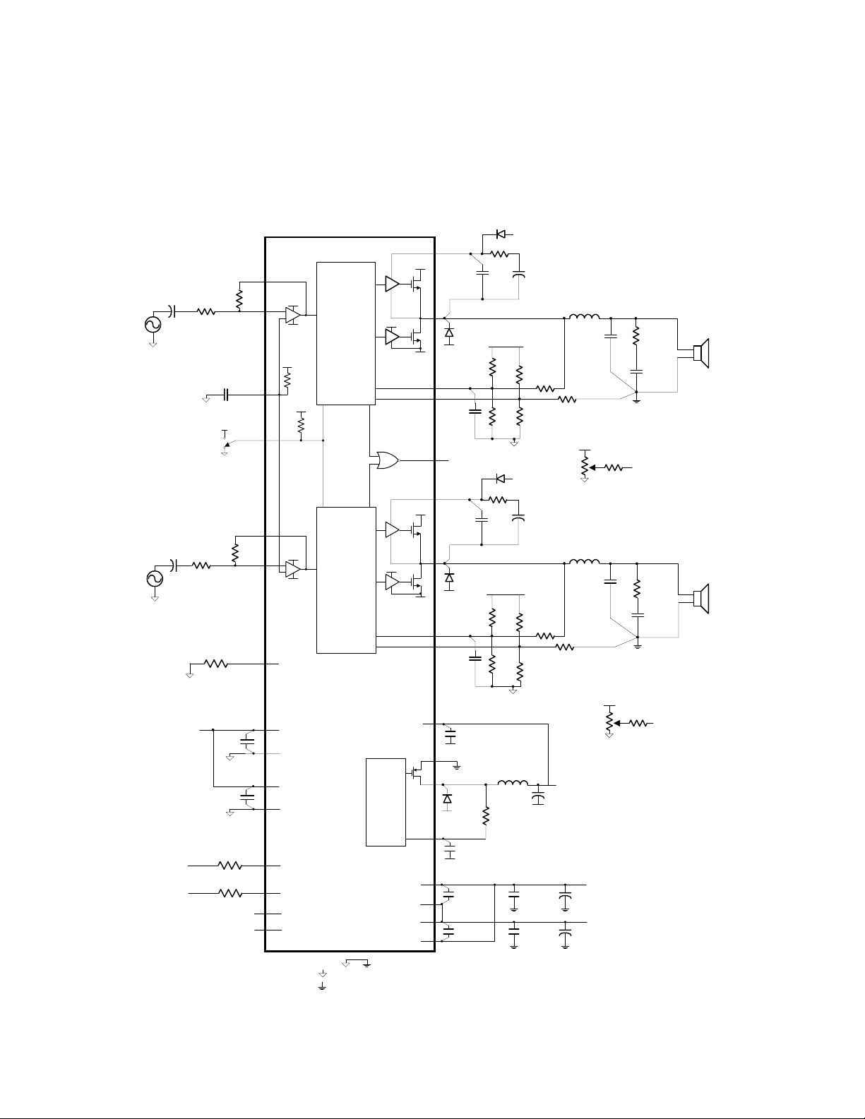
TECHNICAL INFORMATION
Application / Test Diagram
D
11DQ09
OUT1
D
O
MUR120
C
FB
390pF
AGND (Pin 20)
11DQ09
OUT2
D
O
MUR120
C
FB
560pF
AGND (Pin 20)
C
SW
0.1uF,35V
D
SW
11DQ09
C
SWFB
0.1uF,50V
C
HBR
0.1uF,100V
C
HBR
0.1uF,100V
B
RB 250
C
B
0.1uF
V5 (Pin 21)
R
FBA
1K
R
FBB
1.1K
D
B
RB 250
C
B
0.1uF
V5 (Pin 21)
R
FBA
1K
R
FBB
1.1K
100uH, 1A
R
SWFB
1K
Ω
Ω
Ω
L
VN10
+
Ω
VN10
Ω
+
C
Ω
SW
Ω
C
BAUX
47uF
R
FBA
1K
Ω
R
9.1K
R
FBB
1.1K
Ω
BAUX
47uF
R
FBA
1K
Ω
R
9.1K
R
FBB
1.1K
Ω
+
VNN
C
S
0.1uF, 50V
C
S
0.1uF, 50V
FBC
Ω
FBC
Ω
R
9.1K
C
SW
100uF, 35V
C
3.3uF
3.3uF
VNN
VPP
I
+
C
(Pin 20)
I
+
(Pin 20)
R
20K
R
REF
8.25K
R
VNNSENSE
R
VPPSENSE
R
20K
I
5V
I
C
0.1uF
Ω
Ω, 1%
20K
Ω
A
5V
(Pin 20)
R
20K
0.1uF
0.1uF
OAOUT1
R
F
Ω
BIASCAP
OAOUT2
F
Ω
C
S
C
249K
249K
S
INV1
MUTE
INV2
REF
Ω, 1%
Ω, 1%
22
23
2.5V
27
24
25
26
17
21
20
16
15
18
19
6
11
V5
-
+
AGND
200K
Ω
V5
V5
-
+
AGND
V5
AGND
V5
AGND
VNNSENSE
VPPSENSE
NC
NC
TA2022
Processing
&
Modulation
Processing
&
Modulation
VN10
VN10
VN10
Generator
VPP1
VNN1
VNN2
VPP2
VPP1
VNN1
VPP2
VNN2
13
10
31
30
32
1
7
29
28
2
3
5
14
12
9
8
4
VBOOT1
VNN1
(Pin 9)
FBKOUT1
FBKGND1
HMUTE
VBOOT2
VNN2
(Pin 8)
FBKOUT2
FBKGND2
VN10
VNN
VN10GND
VN10SW
VNN
VN10FBK
VNN
L
O
10uH, 10A
0.22uF
R
FBC
9.1K
Ω
V5 (Pin 21)
R
OFA
50K
Ω
AGND (Pin 20)
L
O
10uH, 10A
0.22uF
FBC
Ω
V5 (Pin 21)
R
50K
AGND (Pin 20)
VN10
+
C
S
100uF, 50V
+
C
S
100uF, 50V
VPP
VNN
C
O
R
Z
6.2
2W
Ω,
C
Z
0.22uF
R
OFB
10K
Ω
to FBKGND1
(Pin30)
Offset Trim
Circuit
C
R
O
Z
6.2
Ω,
C
Z
0.22uF
R
OFB
10K
OFA
Ω
Ω
2W
4Ω or 8
to FBKGND2
(Pin28)
Offset Trim
Circuit
R
4Ω or 8
R
L
Ω
L
Ω
Analog Ground
Power Ground
TA2022, Rev. 0.90, 12.00 7 of 27
Page 8

g
TECHNICAL INFORMATION
External Components Description
Components Description
R
Inverting input resistance to provide AC gain in conjunction with RF. This input is
I
RF Feedback resistor to set AC gain in conjunction with RI. Please refer to the Amplifier
CI AC input coupling capacitor which, in conjunction with RI, forms a highpass filter at
R
FBA
R
Feedback divider resistor connected to AGND. This value of this resistor depends
FBB
R
Feedback resistor connected from either the OUT1(2) to FBKOUT1(2) or speaker
FBC
CFB Feedback delay capacitor that both lowers the idle switching frequency and filters
R
Potentiometer used to manually trim the DC offset on the output of the TA2022.
OFA
R
Resistor that limits the manual DC offset trim range and allows for more precise
OFB
R
Bias resistor. Locate close to pin 17 and ground at pin 20.
REF
CA BIASCAP decoupling capacitor. Should be located close to pin 27 and grounded at
CB High frequency bootstrap capacitor, which filters the high side gate drive supply.
C
Bulk bootstrap capacitor that supplements C
BAUX
RB Bootstrap resistor that limits C
DB Bootstrap diode that charges CB, and C
CSW VN10 generator filter capacitors. The high frequency capacitor (0.1uF) must be
LSW VN10 generator filter inductor. This inductor should be sized appropriately so that
D
Flywheel diode for the internal VN10 buck converter. This diode also prevents
SW
C
VN10
SWFB
biased at the BIASCAP voltage (approximately 2.4VDC).
Gain paragraph, in the Application Information section.
)CR2(1f
π=
IIC
Feedback divider resistor connected to V5. This resistor is normally set at 1kΩ.
on the supply voltage setting and helps set the TA2022 gain in conjunction with R
R
F, RFBA,
and R
. Please see the Modulator Feedback Design paragraphs in the
FBC
Application Information Section.
ground to FBKGND1(2). The value of this resistor depends on the supply voltage
setting and helps set the TA2022 gain in conjunction with R
should be noted that the resistor from OUT1(2) to FBKOUT1(2) must have a power
rating of greater than
Design paragraphs in the Application Information Section.
very high frequency noise from the feedback signal, which improves amplifier
performance. The value of C
so that the idle switching difference is greater than 40kHz. Please refer to the
Application / Test Circuit.
adjustment.
pin 20.
This capacitor must be located as close to pin 13 (VBOOT1) or pin1 (VBOOT2) for
reliable operation. The “negative” side of C
(pin 10) or OUT2 (pin 7). Please refer to the Application / Test Circuit.
in a reduction in the average switching frequency.
(bootstrap supply charging).
located close to pin 2 (VN10) to maximize device performance. The bulk capacitor
(100uF) should be sized appropriately such that the VN10 voltage does not
overshoot with respect to VNN during TA2022 turn on.
L
does not saturate, and VN10 does not overshoot with respect to VNN during
SW
TA2022 turn on.
VN10SW from going more than one diode drop negative with respect to VNN.
enerator feedback capacitor. This capacitor, in conjunction with R
(Refer to the Application/Test Circuit)
DISS
2
=
should be offset between channel 1 and channel 2
FB
BAUX
. Please see the Modulator Feedback
)(2RVPPP
FBC
should be connected directly to OUT1
B
during “clipping” events, which result
B
charging current during TA2022 power up
via RB, when the output is low (at VNN).
BAUX
I, RF, RFBA,
, and R
SWFB
. It
FBB
, filters
I,
8 of 27 TA2022, Rev. 0.90, 12.00
Page 9
TECHNICAL INFORMATION
the VN10 feedback signal such that the loop is unconditionally stable.
R
VN10 generator feedback resistor. This resistor sets the nominal VN10 voltage.
SWFB
With R
equal to 1kΩ, the internally VN10 voltage will typically be 11V above
SWFB
VNN.
CS Supply decoupling for the power supply pins. For optimum performance, these
components should be located close to the TA2022 and returned to their respective
ground as shown in the Application/Test Circuit.
R
VNNSNESE
Overvoltage and undervoltage sense resistor for the negative supply (VNN). Please
refer to the Electrical Characteristics Section for the trip points as well as the
hysteresis band.
R
VPPSENSE
Overvoltage and undervoltage sense resistor for the positive supply (VPP). Please
refer to the Electrical Characteristics Section for the trip points as well as the
hysteresis band.
C
Supply decoupling for the high current Half-bridge supply pins. These components
HBR
must be located as close to the device as possible to minimize supply overshoot and
maximize device reliability. These capacitors should have good high frequency
performance including low ESR and low ESL. In addition, the capacitor rating must
be twice the maximum VPP voltage.
CZ Zobel capacitor, which in conjunction with RZ, terminates the output filter at high
frequencies. Use a high quality film capacitor capable of sustaining the ripple current
caused by the switching outputs.
RZ Zobel resistor, which in conjunction with CZ, terminates the output filter at high
frequencies. The combination of R
and CZ minimizes peaking of the output filter
Z
under both no load conditions or with real world loads, including loudspeakers which
usually exhibit a rising impedance with increasing frequency. Depending on the
program material, the power rating of R
may need to be adjusted. The typical
Z
power rating is 2 watts.
DO Fast Recovery diodes that minimize undershoots of the outputs with respect to
power ground during switching transitions as well as output shorts to ground. For
maximum effectiveness, these diodes must be located close to the output pins and
returned to their respective VNN. Please see Application/Test Circuit for VNN return
pin.
LO Output inductor, which in conjunction with CO, demodulates (filters) the switching
waveform into an audio signal. Forms a second order filter with a cutoff frequency
of and a quality factor of
C
O
Output capacitor, which, in conjunction with L
waveform into an audio signal. Forms a second order low-pass filter with a cutoff
frequency of
=
and a quality factor of
π=
)CL2(1f
OOC
.
CLCRQ
OOOL
, demodulates (filters) the switching
O
=
.
Use
CLCRQ
OOOL
a high quality film capacitor capable of sustaining the ripple current caused by the
switching outputs
TA2022, Rev. 0.90, 12.00 9 of 27
Page 10

TECHNICAL INFORMATION
Typical Performance Characteristics – Single Ended
10
f = 1kHz
RL= 4
Ω
5
VPP=|VNN|=31V
AES 17 Filter
2
1
0.5
0.2
THD+N (%)
0.1
0.05
0.02
0.01
0.005
1 2002 5 10 20 50 100
THD+N vs Output Power
Output Power (W)
THD+N (%)
0.005
10
5
2
1
0.5
0.2
0.1
0.05
0.02
0.01
f = 1kHz
RL= 8
Ω
VPP=|VNN|=35V
AES 17 Filter
1
THD+N vs Output Power
2 1005 10 20 50
Output Power (W)
10
Po = 50W/ch
RL = 4
Ω
5
VPP=|VNN|=31V
2
1
0.5
0.2
THD+N (%)
0.1
0.05
0.02
0.01
0.005
20 20k50 100 200 500 1k 2k 5k 10k
+0
19kHz, 20kHz 1:1
-10
Po = 25W/ch, 4
0dBr = 10.0Vrms
-20
VPP=|VNN|=31V
BW = 22Hz - 30kHz
-30
-40
-50
-60
-70
-80
Amplitude (dBr)
-90
-100
-110
-120
-130
-140
20 20k50 100 200 500 1k 2k 5k 10k
Ω
THD+N vs Frequency
BW = 30kHz
BW = 22kHz
Frequency (Hz)
Intermodulation Distortion
Frequency (Hz)
10
Po = 25W/ch
RL = 8
Ω
5
VPP=|VNN|=35V
2
1
0.5
0.2
THD+N (%)
0.1
0.05
0.02
0.01
0.005
20 20k50 100 200 500 1k 2k 5k 10k
+0
19kHz, 20kHz 1:1
-10
Po = 12.5W/ch, 8
0dBr = 10.0Vrms
-20
VPP=|VNN|=31V
BW = 22Hz - 30kHz
-30
-40
-50
-60
-70
-80
Amplitude (dBr)
-90
-100
-110
-120
-130
-140
20 20k50 100 200 500 1k 2k 5k 10k
Ω
THD+N vs Frequency
BW = 30kHz
BW = 22kHz
Frequency (Hz)
Intermodulation Distortion
Frequency (Hz)
10 of 27 TA2022, Rev. 0.90, 12.00
Page 11

TECHNICAL INFORMATION
Typical Performance Characteristics – Single Ended
100
VPP=|VNN|=31V
RL = 4
Ω
90
AES 17 Filter
THD+N < 10%
80
70
60
50
40
Efficiency (%)
30
20
10
0
0 10 20 30 40 50 60 70 80 90 100 110 120
10
f = 1kHz
RL= 4
Ω
5
AES 17 Filter
2
1
0.5
0.2
THD+N (%)
0.1
0.05
0.02
0.01
0.005
1 2002 5 10 20 50 100
-70
VPP=|VNN|=31V
RF=RI=20k
-75
16kFFT
AES 17 Filter
-80
-85
-90
-95
-100
Amplitude (dBr)
-105
-110
-115
-120
20 20k50 100 200 500 1k 2k 5k 10k
Efficiency vs Output Power
Output Power (W)
THD+N vs Output Power
Output Power (W )
Ω
Noise Floor
Frequency (Hz)
+/-27V
+/-23V
+/-31V
100
VPP=|VNN|=35V
RL = 8
Ω
90
AES 17 Filter
THD+N < 10%
80
70
60
50
Efficiency (%)
40
30
20
10
0
0 102030405060 708090
10
f = 1kHz
RL= 8
Ω
5
AES 17 Filter
2
1
0.5
0.2
THD+N (%)
0.1
0.05
0.02
0.01
0.005
1
-40
VPP=|VNN|=31V
-45
Po = 25W/ch, 4
Po = 12.5W/ch, 8
-50
BW = 22Hz - 22kHz
-55
-60
-65
-70
-75
-80
Channel Separation (dBr)
-85
-90
-95
-100
20 20k50 100 200 50 0 1k 2k 5k 10k
Efficiency vs Output Power
Output Power (W)
THD+N vs Output Power
+/-30V
+/-25V
2 1005 10 20 50
Output Power (W)
Channel Separation
Ω
Ω
RL = 4
Ω
RL = 8
Ω
Frequency (Hz)
+/-35V
TA2022, Rev. 0.90, 12.00 11 of 27
Page 12

TECHNICAL INFORMATION
Typical Performance Characteristics - Bridged
10
f = 1kHz
VPP=|VNN|=30V
5
RL= 8Ω BRIDGED
AES 17 Filter
2
1
0.5
0.2
THD+N (%)
0.1
0.05
0.02
0.01
0.005
THD+N (%)
0.005
Amplitude (dBr)
10
0.5
0.2
0.1
0.05
0.02
0.01
+0
-10
-20
-30
-40
-50
-60
-70
-80
-90
-100
-110
-120
-130
-140
2 3005 10 20 50 100 2001
Po = 100W/ch
RL = 8Ω BRIDGED
5
VPP=|VNN|=30V
2
1
20 20k50 100 200 500 1k 2k 5k 10k
19kHz, 20kHz 1:1
Po = 50W/ch, 8Ω BRIDGED
0dBr = 20.0Vrms
VPP=|VNN|=30V
BW = 22Hz - 30kHz
20 20k50 10 0 200 500 1k 2k 5k 10k
THD+N vs Output Power
THD+N vs Frequency
BW = 30kHz
Intermodulation Distortion
Output Power (W )
BW = 22kHz
Frequency (Hz)
Frequency (Hz)
10
f = 1kHz
RL= 8Ω BRIDGED
5
AES 17 Filter
2
1
0.5
0.2
THD+N (%)
0.1
0.05
0.02
0.01
0.005
Efficiency (%)
Amplitude (dBr)
-70
-75
-80
-85
-90
-95
-100
-105
-110
-115
-120
2 3005
1
100
VPP=|VNN|=30V
RL = 8
BRIDGED
Ω
90
AES 17 Filter
THD+N < 10%
80
70
60
50
40
30
20
10
0
0 20 40 60 80 100 120 140 160 180 200 220 240
VPP=|VNN|=30V
RF=RI=20k
Ω
8Ω BRIDGED
16kFFT
AES 17 Filter
20 20k50 100 200 500 1k 2k 5k 10k
THD+N vs Output Power
10 20
Output Power (W )
50 100 200
Efficiency vs Output Power
Output Power (W)
Noise Floor
Frequency (Hz)
+/-27V
+/-23V
+/-30V
12 of 27 TA2022, Rev. 0.90, 12.00
Page 13

TECHNICAL INFORMATION
Application Information
TA2022 Basic Amplifier Operation
The TA2022 has three major operational blocks: the signal processor, the MOSFET driver, and the
power MOSFETs. The signal processor is a 5V CMOS block that amplifies the audio input signal
and converts the audio signal to a switching pattern. This switching pattern is spread spectrum with
a typical idle switching frequency of about 650kHz. The switching patterns for the two channels are
not synchronized and the idle switching frequencies should differ by at least 40kHz to avoid
increasing the audio band noise floor. The idle frequency difference can be accomplished by
offsetting the value of C
560pF for channel 2.
The MOSFET driver level-shifts the signal processor’s 5V switching patterns to the power supply
voltages and drives the power MOSFETs. The MOSFET driver includes a switching power supply
integrated to generate the VN10 supply. Special “bootstrapped” supplies (VBOOT1 and VBOOT2)
are used to power the high side MOSFET drivers. VN10 must be stable (regulated) at 10V to 12V
above VNN. The VN10 circuitry shown in the Application / Test Circuit typically produces 11V
above VNN.
The power MOSFETs are N-channel devices configured in half-bridges and are used to supply
power to the output load. The outputs of the power MOSFETs (OUT1 and OUT2) must be low pass
filtered to remove the high frequency switching pattern. A residual voltage from the switching
pattern will remain on the speaker outputs when the recommended output LC filter is used, but this
signal is outside of the audio band and will not affect audio performance.
Circuit Board Layout
The TA2022 is a power (high current) amplifier that operates at relatively high switching
frequencies. The output of the amplifier switches between VPP and VNN at high speeds while
driving large currents. This high-frequency digital signal is passed through an LC low-pass filter to
recover the amplified audio signal. Since the amplifier must drive the inductive LC output filter and
speaker loads, the amplifier outputs can be pulled above the supply voltage and below ground by
the energy in the output inductance. To avoid subjecting the TA2022 to potentially damaging
voltage stress, it is critical to have a good printed circuit board layout. It is recommended that
Tripath’s layout and application circuit be used for all applications and only be deviated from after
careful analysis of the effects of any changes.
The following components are important to place near their associated TA2022 pins and are ranked
in order of layout importance, either for proper device operation or performance considerations.
- The capacitors C
and will serve to reduce spikes across the supply rails. C
(3mm) of the VNN(8,9) and VPP(4,12) pins. Please note that both VNN1 and VPP1 as
well as VNN2 and VPP2 must be decoupled separately. In addition, the voltage rating for
C
should be 100V as this capacitor is exposed to the full supply range, VPP-VNN.
HBR
- D
, fast recovery PN junction diodes minimize undershoots of the outputs with respect to
O
power ground during switching transitions and abnormal load conditions such as output
shorts to ground. For maximum effectiveness, these diodes must be located close to the
output pins and returned to their respective VNN1(2). Please see Application/Test Circuit
for ground return pin.
for each channel. Typical values of CFB are 390pF for channel 1 and
FB
provide high frequency bypassing of the amplifier power supplies
HBR
should be kept within 1/8”
HBR
TA2022, Rev. 0.90, 12.00 13 of 27
Page 14

TECHNICAL INFORMATION
- C
- C
- C
- D
- To minimize noise pickup and minimize THD+N, R
In general, to enable placement as close to the TA2022, and minimize PCB parasitics, the
capacitors listed above should be surface mount types, located on the “solder” side of the board.
Some components are not sensitive to location but are very sensitive to layout and trace routing.
- To maximize the damping factor and reduce distortion and noise, the modulator feedback
- The output filter capacitor, C
- The modulator feedback resistors, R
TA2022 Grounding
Proper grounding techniques are required to maximize TA2022 functionality and performance.
Parametric parameters such as THD+N, Noise Floor and Crosstalk can be adversely affected if
proper grounding techniques are not implemented on the PCB layout. The following discussion
highlights some recommendations about grounding both with respect to the TA2022 as well as
general “audio system” design rules.
The TA2022 is divided into two sections: the input section, which spans pin 15 through pin 32, and
the output (high power) section, which spans pin 1 through pin 14. On the TA2022 evaluation
board, the ground is also divided into distinct sections, one for the input and one for the output. To
minimize ground loops and keep the audio noise floor as low as possible, the input and output
ground must be only connected at a single point. Depending on the system design, the single point
connection may be in the form of a ferrite bead or a PCB trace.
removes very high frequency components from the amplifier feedback signals and
FB
lowers the output switching frequency by delaying the feedback signals. In addition, the
value of C
is different for channel 1 and channel 2 to keep the average switching
FB
frequency difference greater than 40kHz. This minimizes in-band audio noise.
provides high frequency bypassing for the VN10 (pin 2) and bootstrap supplies. Very
B
high currents are present on these supplies.
filters the feedback signal (VN10FDBK) for the hysteretic VN10 buck converter.
SWFB
The feedback signal is noise sensitive and the trace from C
to VNN should be kept
SWFB
short.
is the flywheel diode for the VN10 buck converter and prevents VN10SW(pin 5) from
SW
going more than one diode drop below VNN.
should be located as close to the
FBC
TA2022 as possible.
connections should be routed directly to the inputs of the output inductors. L
. This was
O
done on the EB-TA2022 board.
, and zobel capacitor, CZ, should be star connected with the
O
load return. The output ground feedback signal should be taken from this star point. This
is suggested by the routing on the Application/Test schematic, but, for space/layout
reasons, this was not fully implemented on the EB-2022.
, R
FBA
, and R
FBB
should all be grounded and
FBC,
attached to 5V together. These connections will serve to minimize common mode noise
via the differential feedback. Please refer to the EB-TA2022 evaluation board for more
information.
14 of 27 TA2022, Rev. 0.90, 12.00
Page 15

TECHNICAL INFORMATION
The analog grounds, pin 15 and pin 20 must be connected locally at the TA2022 for proper device
functionality. On the TA2022 evaluation board, Tripath has used an analog ground plane to
minimize the impedances between pin 15 and pin 20 as well as the other analog ground
connections, such as V5 supply bypassing, and feedback divider networks. The ground for the V5
power supply should connect directly to pin 20. Additionally, any external input circuitry such as
preamps, or active filters, should be referenced to pin 20.
For the power section, Tripath has traditionally used a “star” grounding scheme. Thus, the load
ground returns and the power supply decoupling traces are routed separately back to the power
supply. In addition, any type of shield or chassis connection would be connected directly to the
ground star located at the power supply. These precautions will both minimize audible noise and
enhance the crosstalk performance of the TA2022.
The TA2022 incorporates a differential feedback system to minimize the effects of ground bounce
and cancel out common mode ground noise. As such, the feedback from the output ground for
each channel needs to be properly sensed. This can be accomplished by connecting the output
ground “sensing” trace directly to the star formed by the output ground return, output capacitor, C
and the zobel capacitor, C
Pin 3, VN10GND, is used for the VN10 buck converter. Pin 3 can be connected to the main power
supply decoupling ground trace (or plane) without any loss in functionality or reduction of
performance. This pins is electrically shorted to the copper heat sink (case) of the TA2022. Even if
the internal VN10 regulator is not being used, VN10GND should still be connected to PGND.
TA2022 Amplifier Gain
The gain of the TA2022 is the product of the input stage gain and the modulator gain. Please refer
to the sections, Input Stage Design, and Modulator Feedback Design, for a complete explanation of
how to determine the external component values.
=
A
VTA2022
−≈
. Refer to the Application / Test Circuit for a schematic description.
Z
A* AA
MODULATORV EVINPUTSTAG TA2022V
R
F
R
I
+
R*R
FBBFBA
)R(R*R
FBBFBAFBC
1
+
,
O
For example, using a TA2022 with the following external components,
R
R
R
Input Stage Design
The TA2022 input stage is configured as an inverting amplifier, allowing the system designer
flexibility in setting the input stage gain and frequency response. Figure 1 shows a typical
TA2022, Rev. 0.90, 12.00 15 of 27
= 20kΩ
I
R
= 20kΩ
F
R
= 1kΩ
FBA
= 1.13kΩ
FBB
= 9.09kΩ
FBC
A
VTA2022
20k
Ω
Ω
1.13k Ω*1.0k Ω
−≈
20k
)1.13k(1.0k Ω*9.09k Ω
Ω+
18.13 1
=
+
V
V
Page 16

A
TECHNICAL INFORMATION
application where the input stage is a constant gain inverting amplifier. The input stage gain should
be set so that the maximum input signal level will drive the input stage output to 4Vpp.
TA2022
OAOUT1
V5
-
+
INPUT1
CI
RF
RI
INV1
INPUT2
BIASCAP
INV2
RF
RICI
OAOUT2
GND
V5
+
-
AGND
Figure 1: Input Stage
The gain of the input stage, above the low frequency high pass filter point, is that of a simple
inverting amplifier:
R
F
A
EVINPUTSTAG
−=
R
I
Modulator Feedback Design
The modulator converts the signal from the input stage to the high-voltage output signal. The
optimum gain of the modulator is determined from the maximum allowable feedback level for the
modulator and maximum supply voltages for the power stage. Depending on the maximum supply
voltage, the feedback ratio will need to be adjusted to maximize performance. The values of RFBA,
RFBB and RFBC (see explanation below) define the gain of the modulator. Once these values are
chosen, based on the maximum supply voltage, the gain of the modulator will be fixed even with as
the supply voltage fluctuates due to current draw.
For the best signal-to-noise ratio and lowest distortion, the maximum modulator feedback voltage
should be approximately 4Vpp. This will keep the gain of the modulator as low as possible and still
allow headroom so that the feedback signal does not clip the modulator feedback stage.
Figure 2 shows how the feedback from the output of the amplifier is returned to the input of the
modulator. The input to the modulator (FBKOUT1/FBKGND1 for channel 1) can be viewed as
inputs to an inverting differential amplifier. R
2.5V and R
scales the large OUT1/OUT2 signal to down to 4Vpp.
FBC
FBA
and R
bias the feedback signal to approximately
FBB
16 of 27 TA2022, Rev. 0.90, 12.00
Page 17

TECHNICAL INFORMATION
1/2 TA2022
V5
RFBA
RFBA
RFBB
RFBC
RFBC
OUT1
OUT 1 GROUND
Processing
&
Modulation
FBKOUT1
FBKGND1
RFBB
AGND
Figure 2: Modulator Feedback
The modulator feedback resistors are:
FBA
VPP*R
R
FBA
FBB
=
1Ktypically specified, UserR
Ω=
4)-(VPP
VPP*R
R
FBA
FBC
=
4
A
MODULATOR-V
≈
+
R*R
FBBFBA
1
+
)R(R*R
FBBFBAFBC
The above equations assume that VPP=|VNN|.
For example, in a system with VPP
=36V and VNN
MAX
MAX
=-36V,
R
R
R
= 1kΩ, 1%
FBA
= 1.125kΩ, use 1.13kΩ, 1%
FBB
= 9.0kΩ, use 9.09kΩ, 1%
FBC
The resultant modulator gain is:
)1.13k(1.0k Ω*9.09k Ω
A
MODULATOR-V
≈
Ω+
18.13V/V 1
=+
1.13k Ω*1.0k Ω
Input Capacitor Selection
C
can be calculated once a value for RI has been determined. CI and RI determine the input low
I
frequency pole. Typically this pole is set below 10Hz. C
1
C
I
=
Rf2
IP
π
is calculated according to:
I
TA2022, Rev. 0.90, 12.00 17 of 27
Page 18

TECHNICAL INFORMATION
where:
I
R
= Input resistor value in ohms.
P
f
= Input low frequency pole (typically 10Hz or below).
Mute Control
The mute pin must be driven to a logic low or logic high state for proper operation. The state of the
mute pin is “latched in” to minimize the effects of noise on this pin, which could cause the TA2022
to switch state unintentionally. Controlling the mute pin with a push-pull output from a
mircocontroller, or a physical switch between V5 and AGND, works well as both solutions have low
impedance drive capability. In some cases, it may be desirable to drive the mute pin with an
alternative approach. When the device is in mute, the pin must be “pulled low” via approximately
1kohm to overcome the internal latch and change the TA2022 state (i.e. out of mute). When the
device is not in mute, the mute pin must be “pulled high” via approximately 2kohm to overcome the
internal latch and change the TA2022 state (i.e. into mute). Figure 3 shows a simple control circuit
that buffers a Mute Control signal that is not capable of driving the Mute pin of the TA2022 directly.
When the Mute Control signal is high, the Mute pin will be driven low and theTA2022 will be on. If
the Mute Control signal is low, the 2k resistor will pull the Mute pin high and the TA2022 will be
muted.
V5
2k
TO MUTE
(Pin 24)
MUTE
CONTROL
10k
AGND
Figure 3: Low impedance drive for Mute Pin
To ensure proper device operation, including minimization of turn on/off transients that can result in
undesirable audio artifacts, Tripath recommends that the TA2022 device be muted prior to power
up or power down of the 5V supply. The “sensing” of the V5 supply can be easily accomplished by
using a “mircocontroller supervisor” or equivalent to drive the TA2022 mute pin high when the V5
voltage is below 4.5V. This will ensure proper operation of the TA2022 input circuitry. A microcontroller supervisor such as the MCP101-450 from Microchip Corporation has been used by
Tripath to implement clean power up/down operation.
If turn-on and/or turn-off noise is still present with a TA2022 amplifier, the cause is may be other
circuitry external to the TA2022. While the TA2022 has circuitry to suppress turn-on and turn-off
transients, the combination of power supply and other audio circuitry with the TA2022 in a particular
application may exhibit audible transients. One solution that will completely eliminate turn-on and
turn-off pops and clicks is to use a relay to connect/disconnect that amplifier from the speakers with
that appropriate timing during power on/off.
18 of 27 TA2022, Rev. 0.90, 12.00
Page 19

TECHNICAL INFORMATION
TA2022 Output Capability
The TA2022 can output 100 watts into a 4ohm load at 1% THD+N. The maximum amplifier output
power is determined by a number of factors including the TA2022 junction temperature, the load
impedance and the power supply voltage.
Tripath does not recommend driving loads below 4 ohm as the amplifier efficiency will be seriously
reduced and the amplifier may prematurely current limit.
Bridging the TA2022
The TA2022 is can be bridged by returning the signal from OAOUT1 to the input resistor at INV2.
OUT1 will then be a gained version of OAOUT1, and OUT2 will be a gained and inverted version of
OAOUT1 (see Figure 3). When the two amplifier outputs are bridged, the apparent load impedance
seen by each output is halved, so the minimum recommended impedance for bridged operation is 8
ohms. Due to the internal current limit setting, the maximum supply voltage recommended for
bridged operation is +/-30V. Bridged operation into loads below 8ohms is possible, but, as
mentioned above, the amplifier efficiency will be reduced and the amplifier may prematurely current
limit.
TA2022
OAOUT1
V5
-
+
INPUT
CI
INV1
RF
RI
BIASCAP
20k
INV2
20k
OAOUT2
AGND
V5
+
-
AGND
Figure 4: Input Stage Setup for Bridging
The switching outputs, OUT1 and OUT2, are not synchronized, so a common inductor may not be
used with a bridged TA2022. For this same reason, individual zobel networks must be applied to
each output to load each output and lower the Q of each common mode differential LC filter.
Output Voltage Offset
The output offset voltage of the TA2022 is largely determined by the matching of the respective
R
, R
FBA
, and R
FBB
networks for FBKOUT1(2) and FBKGND1(2). Thus, the intrinsic offset of the
FBC
TA2022 can be altered by the external feedback network resistor matching. To minimize the
nominal untrimmed offset voltage, 1% tolerance resistors are recommended.
In most applications, the output offset voltage will need to be trimmed via an external circuit (either
passive or active). The output offset voltage of the TA2022 can be nulled by modifying the
TA2022, Rev. 0.90, 12.00 19 of 27
Page 20

TECHNICAL INFORMATION
modulator feedback as shown in Figure 4. Potentiometer R
resistance seen by the output ground, and therefore the output offset. ROFB limits the trim range.
1/2 TA2022
V5
RFBA
RFBA
is used to trim the effective
OFA
ROFA
50K
ROFB
10K
RFBC
RFBC
OUT1
OUT 1 GROUND
Processing
&
Modulation
FBKOUT1
FBKGND1
RFBB
RFBB
AGND
Figure 5: Manual Output Offset Trim Circuit
A DC servo can also be used to automatically null any offset voltage. Please see the EB-2022
documentation.
Output Filter Design
Tripath amplifiers generally have a higher switching frequency than PWM implementations allowing
the use of higher cutoff frequency filters, reducing the load dependent peaking/drooping in the
20kHz audio band. This is especially important for applications where the end customer may attach
any speaker to the amplifier (as opposed to a system where speakers are shipped with the
amplifier), since speakers are not purely resistive loads and the impedance they present changes
over frequency and from speaker model to speaker model. An RC network, or “zobel” (R
should be placed at the filter output to control the impedance “seen” by the TA2022. The TA2022
works well with a 2
nd
order, 80kHz LC filter with LO = 10uH and CO = 0.22uF and RZ = 6ohm and CZ
, CZ)
Z
= 0.22uF.
Output inductor selection is a critical design step. The core material and geometry of the output
filter inductor affects the TA2022 distortion levels, efficiency, power dissipation and EMI output.
The inductor should have low loss at 700kHz with 80Vpp. Tripath has used:
- Micrometals (www.micrometals.com) type-2 toroidal iron powder cores, which have low
loss, good linearity and low EMI radiation. The specific core was a T106-2 wound to
11uH with 16AWG wire. Tripath has also used T94-2 cores wound to 11uH with good
success.
- JW Miller 5502 10uH rod core inductors, which have excellent linearity, approximately 1
watt of core loss and high EMI radiation.
- ISI RPC-100-10 10uH vertical rod core inductors, which have good linearity, medium core
loss and high EMI radiation.
20 of 27 TA2022, Rev. 0.90, 12.00
Page 21

TECHNICAL INFORMATION
Power Supplies
The TA2022 requires the split supply rails VPP1(VPP2) and VNN1(VNN2), and V5. It also uses
some additional voltages, VN10, VBOOT1 and VBOOT2 that are generated internally. The
selection of components for the switching regulator is shown in the Application / Test Diagram.
Minimum and Maximum Supply Voltage Operating Range
The TA2022 can operate over a wide range of power supply voltages from +/-12V to +/-36V. In
order to optimize operation for either the low or high range, the user must select the proper values
for R
VNNSENSE
, R
VPPSENSE
, R
FBA
, R
, and R
FBB
. Please refer to the Modulator Feedback Design and
FBC
Over/Under-voltage Protection sections for more additional information.
VN10 (Pin 2)
The TA2022 has an internal hysteretic buck converter, which, in conjunction with a handful of
passive components, generates the necessary floating power supply for the mosfet driver stage
(nominally 11V with the external components shown in Application / Test Circuit). The performance
curves shown in the data sheet as well as efficiency measurements were done using the internal
VN10 generator. Tripath recommends that the internal VN10 generator be used.
In some cases, though, a designer may wish to use an external VN10 generator. The specification
for VN10 quiescent current (65mA typical, 80mA maximum) in the Electrical Characteristics section
states the amount of current needed when an external floating supply is used. If the internal VN10
generator is not used, Tripath recommends shorting VN10SW(pin 5) to VN10GND(pin 3) and
VN10FDBK(pin 14) to VN10GND(pin 3). VN10GND should still be connected to the system power
(high current) ground star for noise reasons.
The external VN10 supply must be able to source a maximum of 80mA into the VN10 pin. Thus, a
positive supply must be used. In addition, this supply must be referenced to the VNN rail. If the
external VN10 supply does not track fluctuations in the VNN supply or is not able to source current
into the VN10 pin, the TA2022 will, at the very least, not work, but more likely, be permanently
damaged.
Figure 6 shows a simple circuit for an external VN10 supply. Though simple, there is one problem
with this circuit; the maximum input voltage of the 7810. If the maximum input voltage of the 7810
is exceeded (typically this voltage is 35V), then the 7810 will be damaged which will likely cause
damage to the TA2022. Thus, this circuit should only be used where the VNN power supply is well
regulated even under heavy load conditions (including the effects of power supply pumping).
TO POWER SUPPLY
"STAR" GND
VIN
0.1uF 0.1uF10uF
7810
"GND"
TO VNN (PIN 8,9)
VOUT
TO VN10 (PIN 2)
10uF
Figure 6: Simple External VN10 Supply
TA2022, Rev. 0.90, 12.00 21 of 27
Page 22

TECHNICAL INFORMATION
Figure 7 shows a much more robust VN10 supply. In this case, the maximum supply differential the
LM317 experiences is the input voltage minus the output voltage. The maximum differential
specification is 40V for the LM317. W hen used as the VN10 supply for the TA2022, the maximum
differential the LM317 will experience is 25V, even at maximum operating voltage of 36V for the
TA2022. As configured, VOUT will be about 10.63V above VNN.
TO POWER SUPPLY
"STAR" GND
10uF
0.1uF
VIN
ADJ
1.8k
TO VNN (PIN 8,9)
LM317
10uF
VOUT
240
0.1uF
TO VN10 (PIN 2)
10uF
Figure 7: Robust External VN10 Supply
It should be noted that the maximum power dissipation for either Figure 6 or Figure 7 is:
MAX
1.6W80mA(max.)11V)(31VIOUTVOUT)(VINPD
=×−≈×−=
Thus, the LM7810 or LM317 must be sufficiently heat sinked to sustain 80mA in the system
ambient temperature. In the case where multiple TA2022’s are run off the same VN10 generator,
the power dissipation may be prohibitively large for the linear regulator in conjunction with allowable
heat sink. In these cases, a more sophisticated scheme using an additional transformer secondary
winding referenced to VNN may be necessary to minimize the linear regulator power dissipation.
Protection Circuits
The TA2022 is guarded against over-current, over / under-voltage and over-temperature conditions.
If the device goes into an over-current or over / under-voltage condition, the HMUTE goes to a logic
HIGH indicating a fault condition. When this occurs, the amplifier is muted, all outputs are TRISTATED, and will float to approximately 2.5VDC.
Over-current Protection
An over-current fault occurs if more than approximately 8 amps of current flows from any of the
amplifier output pins. This can occur if the speaker wires are shorted together or if one side of the
speaker is shorted to ground. An over-current fault sets an internal latch that can only be cleared if
the MUTE pin is toggled or if the part is powered down. See the over-current curves in the Typical
Characteristics section for more information.
Over / Under-voltage Protection
The TA2022 has built-in over and under voltage protection for both the VPP and VNN supply rails.
The nominal operating voltage will typically be chosen as the supply “center point.” This allows the
supply voltage to fluctuate, both above and below, the nominal supply voltage.
22 of 27 TA2022, Rev. 0.90, 12.00
Page 23

TECHNICAL INFORMATION
VPPSENSE (pin 19) performs the over and undervoltage sensing for the positive supply, VPP.
VNNSENSE (pin 18) performs the same function for the negative rail, VNN. In the simplest
implementation, the supply is done via a single, external resistor per sense pin. When the current
through R
VPPSENSE
(or R
VNNSENSE
) goes below or above the values shown in the Electrical
Characteristics section (caused by changing the power supply voltage), the TA2022 will be muted.
VPPSENSE is internally biased at 2.5V and VNNSENSE is biased at 1.25V. For the single resistor
sense case (as shown in the Application / Test Diagram), these bias points must be taken into
consideration when calculating the R
VPPSENSE
or R
VNNSENSE
resistor.
Once the supply comes back into the supply voltage operating range (as defined by the supply
sense resistors), the TA2022 will automatically be unmuted and will begin to amplify. There is a
hysteresis range on both the VPPSENSE and VNNSENSE pins. If the amplifier is powered up in
the hysteresis band the TA2022 will be muted. Thus, the usable supply range is the difference
between the over-voltage turn-off and under-voltage turn-off for both the VPP and VNN supplies. It
should be noted that there is a timer of approximately 200mS with respect to the over and under
voltage sensing circuit. Thus, the supply voltage must be outside of the user defined supply range
for greater than 200mS for the TA2022 to be muted.
The equation for calculating R
VPPSENSE
is as follows:
2.5V - VPP
R
VPPSENSE
=
I
VPPSENSE
The equation for calculating R
VNNSENSE
is as follows:
R
VNNSENSE
=
I
VNNSENSE
VNN-1.25V
where I
VPPSENSE
or I
VNNSENSE
can be any of the currents shown in the Electrical
Characteristics table for VPPSENSE and VNNSENSE, respectively.
Example: Nominal supply voltage – +/-32.5V +/-10%
From this information, a value of R
VPPSENSE
and R
VNNSENSE
can be calculated using the above
formulas.
MAX
=×=
36V use35.75V1.132.5VVPP
MAX
−=×−=
36V- use35.75V1.132.5VVNN
R
where I
VPPSENSE
VPPSENSE
2.5V -36V
A138
µ
kΩ
%1,k243use242.75
Ω==
is the minimum over-voltage turn off current for VPPSENSE.
R
where I
VNNSENSE
VNNSENSE
36V- -1.25V
A152
µ
kΩ
%1,k249use245.1
Ω==
is the minimum over-voltage turn off current for VNNSENSE.
TA2022, Rev. 0.90, 12.00 23 of 27
Page 24

TECHNICAL INFORMATION
Using the resistor values from above, the actual minimum over voltage turn off points will be:
N_OFFMIN_OV_TUR
N_OFFMIN_OV_TUR
µ
A
36.03V2.5V138kΩ243VPP
=+×=
36.60V-A152kΩ4921.25VVNN
=×−=
µ
The other three trip points can be calculated using the same formula but inserting the appropriate
I
VPPSENSE
(or I
VNNSENSE
) current value. As stated earlier, the usable supply range is the difference
between the minimum overvoltage turn off and maximum under voltage turn-off for both the VPP
and VNN supplies.
=
=
VPP-VPPVPP
VNN-VNNVNN
N_OFFMAX_UV_TURN_OFFMIN_OV_TUR RANGE
N_OFFMAX_UV_TURN_OFFMIN_OV_TUR RANGE
Using the resistor values from above, and the maximum under voltage trip currents shown in the
Electrical Characteristics table, the maximum under voltage turn off points will be:
N_OFFMAX_UV_TUR
N_OFFMAX_UV_TUR
µ
A
µ
23.64V2.5V87kΩ243VPP
=+×=
22..41V-A95kΩ4921.25VVNN
=×−=
and the resultant supply ranges will be:
RANGE
RANGE
12.39V23.64V03.36VPP
=−=
14.19V-22.41V60.36VNN
=−−−=
It should also be noted that the tolerance of the R
VPPSENSE
(or R
VNNSENSE
voltages and thus, the usable supply range. To minimize the additional variance Tripath
recommends 1% tolerance resistors.
As a matter of completeness, the formulas below include the effect of resistor tolerance assuming a
known value of R
VPPSENSE
or R
VNNSENSE
.
TRIPVPPSENSE N_OFFMIN_OV_TUR
TRIPVPPSENSE N_OFFMAX_UV_TUR
TRIPVNNSENSE N_OFFMIN_OV_TUR
TRIPVNNSENSE N_OFFMAX_UV_TUR
+÷×−=
+××−=
Using a value of 243kΩ for R
VPPSENSE
along with the appropriate value of I
and a value of 249kΩ for R
, the trip voltages and supply ranges can be calculated.
TRIP
VNNSENSE
N_OFFMIN_OV_TUR
N_OFFMAX_UV_TUR
RANGE
=−=
µ
AkΩ
µ
Ak Ω
9.74V24.70V44.34VPP
) resistors will effect the trip
2.5V)100/TOL1()IR(VPP
++÷×=
2.5V)100/TOL1()IR(VPP
++××=
)100/TOL1()IR(25.1VNN
)100/TOL1()IR(25.1VNN
, assuming 5% tolerance,
34.44V 2.5V)100/51()138243(VPP
=++÷×=
24.70V 2.5V)100/51()87243(VPP
=++××=
24 of 27 TA2022, Rev. 0.90, 12.00
Page 25

TECHNICAL INFORMATION
(
)
N_OFFMIN_OV_TUR
N_OFFMAX_UV_TUR
RANGE
=−−−=
µ
µ
11.21V-23.59V80.34VNN
−=+××Ω−=
80.34)100/51()152492(25.1VNN
−=+÷×Ω−=
59.23)100/51()95492(25.1VNN
VAk
VAk
Thus, by using 5% resistors, the supply range for the VPP has been reduced by 2.65V while the
VNN range has been reduced by approximately 3.0V (as compared to resistors with no tolerance
variation). In actuality, if a 5% resistor was to be used, then the initial value of R
R
VNNSENSE
would have had to be adjusted such that the minimum over voltage turn off points would
VPPSENSE
and
have never been less than +/-36V as defined by the supply voltage and tolerance specification.
It should be noted that the values for V
VPPSENSE
Characteristics table were calculated using a value of 249kΩ for both R
and V
VNNSENSE
shown in the Electrical
VPPSENSE
and R
VNNSENSE
. In
addition, for the maximum and minimum values, as opposed to the typical ones, a 1% tolerance
resistor value around 249kΩ was chosen to show the effect on supply range. Thus, the minimum
and maximum values would be “worst case” assuming a supply voltage of 5V for the input section
of the TA2022.
Over-temperature Protection
An over-temperature fault occurs if the junction temperature of the part exceeds approximately
165°C. The thermal hysteresis of the part is approximately 30°C, therefore the fault will
automatically clear when the junction temperature drops below 135°C.
HMUTE (pin 32)
The HMUTE pin is a 5V logic output that indicates various fault conditions within the device. These
conditions include: over-current, overvoltage and undervoltage. The HMUTE output is capable of
directly driving an LED through a series 2k
resistor.
Ω
Heat Sink Requirements
In most applications it will be necessary to fasten the TA2022 to a heat sink. The determining factor
is that the 150°C maximum junction temperature, T
(max) cannot be exceeded, as specified by the
J
following equation:
TT
−
P
DISS
=
θ
A)MAX(J
JA
where:
P
= maximum power dissipation
DISS
T
= maximum junction temperature of TA2022
JMAX
T
= operating ambient temperature
A
= junction-to-ambient thermal resistance
θ
JA
=
θ
θ
JA
JC + θCS + θSA
TA2022, Rev. 0.90, 12.00 25 of 27
Page 26

(
)
TECHNICAL INFORMATION
Example:
What size heat sink is required to operate the TA2022 at 80W per channel continuously in a 70ºC
ambient temperature?
P
Efficiency =
Thus, P
The
θ
(assuming a
music source (as opposed to a continuous sine wave) and regulatory agency testing requirements
will determine the size of the heat sink required.
is determined by:
DISS
P
OUT
η
=
P
IN
(per channel) =
P
DISS
for two channels = 28.24W
DISS
TT
−
DISS
A)MAX(J
=
=
θ
JA
P
of the TA2022 is 1.0°C/W, so a heat sink of 1.63°C/W is required for this example
JC
= 0.2°C/W). In actual applications, other factors such as the average P
θ
CS
P
70150
−
24.28
P
=
OUT
P
η
= 2.83°C/W
OUT
−
OUT
PP
DISSOUT
80
85.0
14.12W80
=−=−
with a
DISS
26 of 27 TA2022, Rev. 0.90, 12.00
Page 27

TECHNICAL INFORMATION
Performance Measurements of the TA2022
The TA2022 operates by generating a high frequency switching signal based on the audio input.
This signal is sent through a low-pass filter (external to the Tripath amplifier) that recovers an
amplified version of the audio input. The frequency of the switching pattern is spread spectrum in
nature and typically varies between 100kHz and 1MHz, which is well above the 20Hz – 20kHz
audio band. The pattern itself does not alter or distort the audio input signal, but it does introduce
some inaudible components.
The measurements of certain performance parameters, particularly noise related specifications
such as THD+N, are significantly affected by the design of the low-pass filter used on the output as
well as the bandwidth setting of the measurement instrument used. Unless the filter has a very
sharp roll-off just beyond the audio band or the bandwidth of the measurement instrument is limited,
some of the inaudible noise components introduced by the TA2022 amplifier switching pattern will
degrade the measurement.
One feature of the TA2022 is that it does not require large multi-pole filters to achieve excellent
performance in listening tests, usually a more critical factor than performance measurements.
Though using a multi-pole filter may remove high-frequency noise and improve THD+N type
measurements (when they are made with wide-bandwidth measuring equipment), these same
filters degrade frequency response. The TA2022 Evaluation Board uses the Application/Test
Circuit of this data sheet, which has a simple two-pole output filter and excellent performance in
listening tests. Measurements in this data sheet were taken using this same circuit with a limited
bandwidth setting in the measurement instrument.
TA2022, Rev. 0.90, 12.00 27 of 27
Page 28

TECHNICAL INFORMATION
Package Information
32-pin SSIP Package:
28 of 27 TA2022, Rev. 0.90, 12.00
Page 29

TECHNICAL INFORMATION
ADVANCED INFORMATION – This is a product in development. Tripath Technology Inc. reserves
the right to make any changes without further notice to improve reliability, function or design.
Tripath and Digital Power Processing are trademarks of Tripath Technology Inc. Other trademarks,
which are referenced in this document, are owned by their respective companies
Tripath Technology Inc. reserves the right to make changes without further notice to any products
herein to improve reliability, function or design. Tripath does not assume any liability arising out of
the application or use of any product or circuit described herein; neither does it convey any license
under its patent rights, nor the rights of others.
TRIPATH’S PRODUCTS ARE NOT AUTHORIZED FOR USE AS CRITICAL COMPONENTS IN
LIFE SUPPORT DEVICES OR SYSTEMS WITHOUT THE EXPRESS WRITTEN CONSENT OF
THE PRESIDENT OF TRIPATH TECHNOLOGY INC. As used herein:
1. Life support devices or systems are devices or systems which, (a) are intended for surgical
implant into the body, or (b) support or sustain life, and whose failure to perform, when properly
used in accordance with instructions for use provided in this labeling, can be reasonably
expected to result in significant injury to the user.
2. A critical component is any component of a life support device or system whose failure to
perform can be reasonably expected to cause the failure of the life support device or system, or
to affect its safety or effectiveness.
For more information on Tripath products, visit our web site at:
World Wide Sales Offices
Western United States: Jim Hauer jhauer@tripath.com 408-567-3089
Taiwan, HK, China: Jim Hauer jhauer@tripath.com 408-567-3089
Japan: Osamu Ito ito@tripath.com 81-42-334-2433
Europe: Steve Tomlinson stomlinson@tripath.com 44-1672-86-1020
www.tripath.com
.
B
TRIPATH TECHNOLOGY, INC.
3900 Freedom Circle, Suite 200
Santa Clara, California 95054
408-567-3000
TA2022, Rev. 0.90, 12.00 29 of 27
 Loading...