

Datasheet T835-400B, T835-600B, T810-600B, T810-400B Datasheet (SGS Thomson Microelectronics)
Page 1
T810-xxxB
®
FEATURES
I
= 8 A
TRMS
SENSITIVE GATE : I
10mA and 35mA
GT ≤
HIGH COMMUTATION T E CHNOLO GY
HIGH I
CAPABILITY
TSM
DESCR IPT ION
The T810-xxxB and T835-xxxB series are using
high performance TOPGLASS PNPN technology.
These devices are intented for AC control applications, using surface mount technology where high
commutating and surge performances are required (like power tools, Solid State Relay).
ABSOLUTE MAXIMUM RATINGS
T835-xxxB
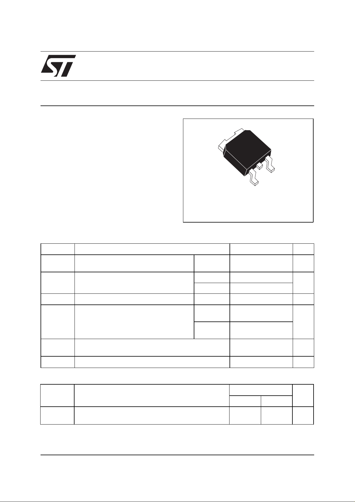
HIGH PERFORMANCE TRIACS
A2
A2
A1
DPAK
(Plastic)
G
Symbol Parameter Value Unit
I
T(RMS)
RMS on-state current
Tc =110 °C8 A
(360° conduction angle)
I
TSM
Non repetitive surge peak on-state current
( Tj initial = 25°C )
2
t
I
dI/dt
2
I
t value for fusing
Critical rate of rise of on-state current
I
G
= 50mA diG/dt = 0.1A/µs
tp = 8.3 ms 85 A
tp = 10 ms 80
tp = 10 ms 32 A
Repetitive
20 A/µs
F = 50 H z
Non
100
2
Repetitive
Tstg
Tj
T
Storage temperature range
Operating junction temperature range
Maximum temperature for soldering during 10 s
- 40 t o + 150
- 40 t o + 125
260 °C
°C
°C
Symbol Parameter T810-/T835- Unit
400B 600B
V
V
DRM
RRM
Repetitive peak off-state voltage
Tj = 125 °C
400 600 V
s
May 1998 Ed : 1A
1/5
Page 2
T810-xxxB / T835-xxxB
THERMAL RES IST ANCE S
Symbol Parameter Value Unit
Rth (j-c)
Rth (j-c)
Rth (j-a)
Junction to case for DC
Junction to case for AC 360° conduction angle ( F= 50 Hz)
2
Junction to ambient (S = 0.5 cm
)
2.1 °C/W
1.6 °C/W
70 °C/W
GATE CHARACTERISTI CS (maximum values)
P
= 1 W PGM= 10 W (tp = 20 µs) IGM = 4 A (tp = 20 µs)
G(AV)
ELECTRICAL CHARACTERIST ICS
Symbol Test Conditions Quadrant Suffix Unit
T810 T835
I
GT
V
GT
V
GD
I
L
*
I
H
V
TM
I
DRM
I
RRM
VD=12V (DC) RL=33Ω
VD=12V (DC) RL=33Ω
VD=V
IG=1.2 I
I
= 100mA gate open
T
*
I
= 11A tp= 380µs
TM
V
DRM
V
RRM
RL=3.3kΩ
DRM
GT
Rated
Rated
Tj=25°C I-II-III MAX 10 35 mA
Tj=25°CI-II-IIIMAX 1.3 V
Tj=125°C I-II-III MIN 0.2 V
Tj=25°C I-II-III MAX 25 60 mA
Tj=25°C MAX 15 35 mA
Tj=25°CMAX1.5V
Tj=25°CMAX10µA
Tj=125°CMAX2mA
dV/dt *
Linear slope up to
=67%V
V
D
DRM
Tj=125°C MIN 50 500 V/µs
gate open
(dI/dt)c *
(dV/dt)c = 0.1V/µs
(dV/dt)c = 15V/µs
* For either polarity of electrode A2 voltage with reference to electrode A1.
Tj=125°C MIN 5.4 9 A/ms
Tj=125°C MIN 2.7 4.5 A/ms
ORDERING INFORMATION Add "-TR" suffix for Tape and Reel shipment
TRIAC
T
8 10 -
600
VOLTAGE
B
CURRENT
S ENSITIVITY
2/5
PACKAGE
B = DPAK
Page 3

T810-xxxB / T835-xxx B
Fig 1a: Maximum power dissipation versus RMS
on-state current (T810 only).
P(W)
10
8
6
4
2
α
0
012345678
α
α
I (A)
T(RMS)
α
α
180°
α
α
Fig 2: Correlation between maximum power dissipation and maximum allowable temperatures
(Tamb and Tcase) for different thermal resistances
heatsink+contact.
P(W)
10
8
6
Rth=15 °C/W
4
2
0
0 25 50 75 100 125
Rth=10 °C/W
α
Tamb(°C)
Rth=5°C/W
Tcase (°C)
110
Rth=0°C/W
115
120
125
Fig 1b: Maximum power dis sipation versus RMS
on-state current. (T835 only)
P(W)
10
8
6
4
2
0
012345678
α
α
α
I (A)
T(RMS)
α
α
180°
α
α
Fig 3: RMS on-state current versus ambient temperature.
I (A)
T(RMS)
9
8
7
6
5
4
3
2
1
0
0 25 50 75 100 125
Tamb(°C)
α
Fig 4: Relative variation of thermal impedance
junction to case versus pulse duration.
K=[Zth(j-c)/Rth(j-c)]
1.0
0.5
0.2
0.1
1E-3 1E-2 1E-1 1E+0
tp(s)
Fig 5: Relative variation of gate trigger current and
holding current versus junction temperature (typical values).
I ,I [Tj]/I ,I [Tj=25°C]
GT H GT H
2.5
2.0
I
1.5
1.0
0.5
0.0
-40 -20 0 20 40 60 80 100 120 140
GT
I
H
Tj(°C)
3/5
Page 4

T810-xxxB / T835-xxxB
Fig 6: Non repetitive surge peak on-state current
versus number of cycles.
I (A)
TSM
80
70
Tj initial=25°C
F=50Hz
60
50
40
30
20
10
0
1 10 100 1000
Number of cycles
Fig 8: On-state characteristics (maximum val ues).
I (A)
TM
100.0
Tj max.:
10.0
Tj=Tj max.
Vto=0.8V
Rt=60m
Ω
Fig 7: Non repetitive surge peak on-state current
for a sinusoidal pulse with width tp<10ms, and c orresponding value of I
I (A),I²t(A²s)
TSM
500
100
10
12 510
2
t.
Tj initial=25°C
ITSM
I²t
tp(ms)
Fig 9: Thermal resistance junction to ambient versus copper surface under tab (Epoxy printed c ircuit
board FR4, copper thickness: 35µm).
Rth(j-a) (°C/W)
100
80
60
1.0
0.1
0.0 0.5 1.0 1.5 2.0 2.5 3.0 3.5 4.0 4.5 5.0
Tj=25°C
V (V)
TM
40
20
S(Cu) (cm²)
0
0 2 4 6 8 10 12 14 16 18 20
4/5
Page 5

PACKAGE ME CHANICAL D AT A
DPAK Plastic
E
B2
L2
H
L4
B
G
0.60MIN.
A2
V2
T810-xxxB / T835-xxx B
REF. DIMENSIONS
Millimeters Inches
A
C2
D
A1
C
Min. Typ. Max Min. Typ. Max.
A 2.20 2.40 0.086 0.094
A1 0.90 1.10 0.035 0.043
A2 0.03 0.23 0.001 0.009
B 0.64 0.90 0.025 0.035
B2 5.20 5.40 0.204 0.212
C 0.45 0.60 0.017 0.023
C2 0.48 0.60 0.018 0.023
D 6.00 6.20 0.236 0.244
E 6.40 6.60 0.251 0.259
G 4.40 4.60 0.173 0.181
H 9.35 10.10 0.368 0.397
L2 0.80 0.031
L4 0.60 1.00 0.023 0.039
V2 0° 8° 0° 8°
FOOT PRINT (millimeters)
6.7
WEIGHT : 0.30g
MARKING
6.7
6.7
3
1.61.6
2.32.3
Information furnished is believed to be accurate and reliable. However, STMicroelectronics assumes no responsibility for the consequences of
use of such information nor for any infringement of patents or other rights of third parties which may result from its use. No license is granted by
implication or otherwis e under any patent or patent rights of STMicroelectro nics. Specifications men tioned in this publication are subject to
change without notice. This publication supersedes and replaces all information previously supplied.
STMicroelectro nic s products are not authorized for use as critical components in li fe s upport devices or systems without express w ri tt en approval of STMicroelectronics.
© 1998 STMicroelectronics - Printed in Italy - All rights reserved.
STMicroelectronics GROUP OF COMPANIES
Australia - Brazil - Canada - China - France - Germany - Italy - Japan - Korea - Malaysia - Malta - Mexico - Morocco - The
Netherlands - Singapore - Spain - Sweden - Switzerland - Taiwan - Thailand - United Kingdom - U.S.A.
TYPE MARKING
T810-400B
T810-600B
T835-400B
T835-600B
1040
1060
3540
3560
T8
T8
T8
T8
5/5
 Loading...