

Page 1
Rev.
Date
Page
Comment
First Edition
Mar 27, 2002
Final Revision
******
OP T R E X
LCD Module Technical Specification
T-51446L050J-FW-P-AB
Tentative
Table of Contents
1. Applications
2. Features
3. Mechanical Specifications
4. Mechanical Drawing TFT LCD Module
5. Input / Output Terminals
6. Absolute Maximum Ratings
7. Electrical Characteristics
8. Power Sequence
9. Optical Characteristics
10. Handling cautions
11. Reliability TEST
12. Labeling
13. Block Diagram
Revision History
........................................................................................................................................
.......................................................................................................................................
Checked by (Quality Assurance Div.)
Checked by (Design Engineering Div.)
Prepared by (Production Div.)
.................................................................................................................................
................................................................................................
..................................................................
..................................................................................................
..............................................................................................
.....................................................................................................
..................................................................................................................
......................................................................................................
................................................................................................................
.....................................................................................................................
.........................................................................................................................
2
2
2
3
4
6
6
15
16
19
20
20
21
T-51446L050J-FW-P-AB
OPTREX CORPORATION
Page 1/21
Page 2

1. Application
This technical specification applies to 5” color TFT-LCD module. The applications of the
panel are car TV , portable DVD and GPS.
2. Features
. Compatible with NTSC & PAL system
. Pixel in stripe configuration
. Slim and compact
. Vcom Toggle
. Image Reversion : Up/Down and Left/Right
3. Mechanical Specifications
Parameter Specifications Unit
Screen Size 5 (diagonal) inch
Display Format
Active Area
Dot Pitch
Pixel Configuration Stripe
Outline Dimension
Weight 160±10 g
102.72 (H)×74.53 (V)
127.4 (W)×92.8 (H)×12.9 (D)(typ.)
960×234
0.107 (H)×0.319 (V)
dot
mm
mm
mm
T-51446L050J-FW-P-AB
OPTREX CORPORATION
Page 2/21
Page 3
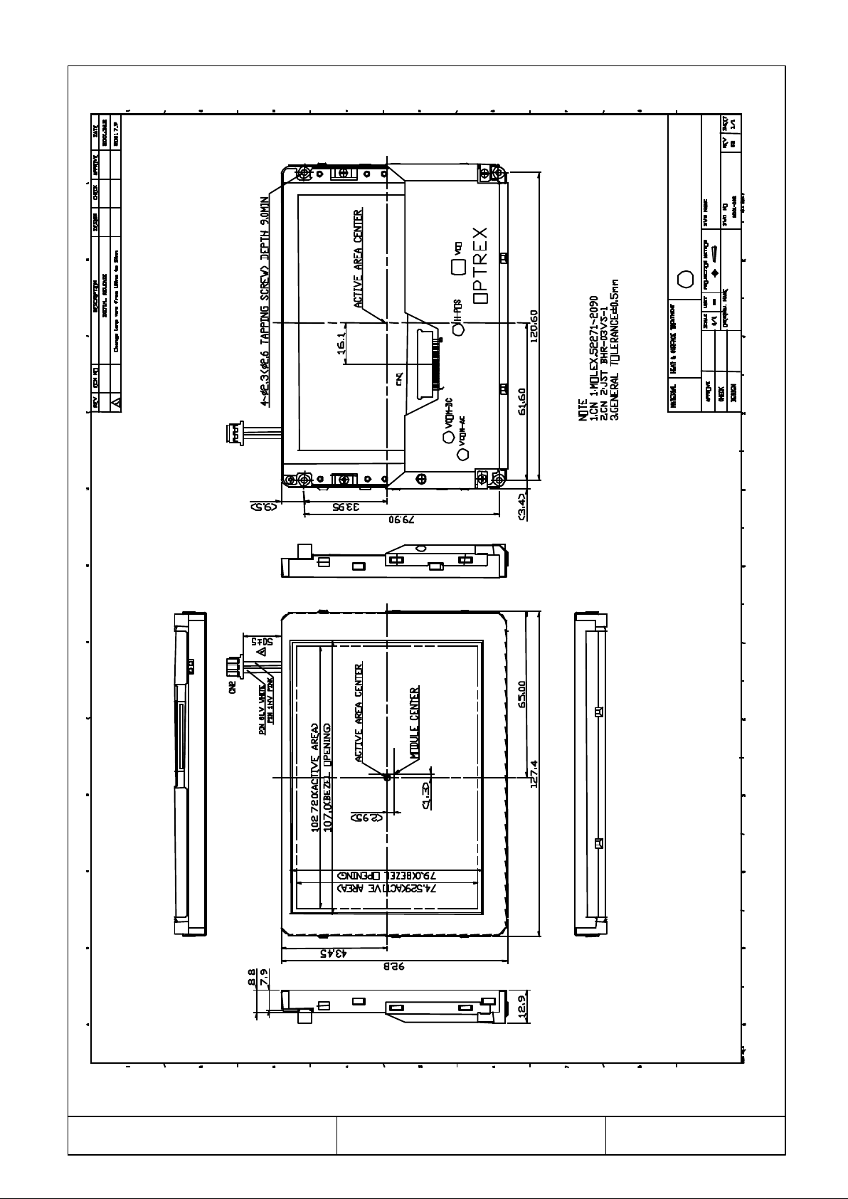
4. Mechanical Drawing of TFT-LCD Module
T-51446L050J-FW-P-AB
OPTREX CORPORATION
Page 3/21
Page 4
5. Input / Output Terminals
5-1) TFT-LCD Panel Driving
Pin No Symbol I/O Description Remark
1 HSY I/O Horizontal Sync. Input / Output
2 FRP O Video Polarity Alternating Signal
3 CSY/HSY I Composite Sync. Signal Note 5-1
4 V
5 V
6 V
7 V
8 V
GH
GL
B
R
G
I Supply Voltage for Gate Driver (Hi level) Note 5-2
I Supply Voltage for Gate Driver (Low level) Note 5-3
I Video Signal (Blue)
I Video Signal (Red)
I Video Signal (Green)
9 GND I Ground
10 V
11 V
DD
CC
I Supply voltage for Controller Note 5-4
I Supply voltage for source driver Note 5-5
12 GND I Ground
13 CKC I Control pin for select I/O signal Note 5-1
14
VSY
I/O Vertical Sync. Input/ Output
15 PSI O Synchronize Pulse for Decoder
16 PSC O Synchronize Pulse for DC-DC Converter
17 NC I No Connection /Vertical sync. Signal Note 5-1
18 UD I UP/DOWN Control Note 5-7
19 RL I Right/Left Shift Control Note 5-6
20 NP I/O NTSC/PAL Selection Signal(Low : PAL, High : NTSC) Note 5-8
Note 5-1-1 : PVI’S module can support 2 input mode .
CKC of 26 pin select 2 input mode.
Parameter Select pin(CKC) Description
CKC CSY/HD NC/VD
Composite sync mode High CSY (positive edge) -
Sync separate mode Low HD(negative edge) VD(positive edge)
Note 5-1-2The default mode of PVI module is composite sync mode (CKC= high)
Note 5-1-3: If you use sync separate mode (CKC= low),please contact PVI.
Note 5-2:VGHTYP.=+17V
Note 5-3:VGLTYP.=-15V
T-51446L050J-FW-P-AB
OPTREX CORPORATION
Page 4/21
Page 5
Note 5-4:VDDTYP.=+5V
Note 5-5:VCCTYP.=+5V
Note 5-6 : Low (0V) for shift Right; Input Hi (+5.0V) for inverse (shift Left).
Note 5-7 : Hi (+5.0V) for DOWN; Low (0V) for UP.
Note 5-8 : PAL= LOW(0V),NTSC= Hi(+5.0V) :
( If use auto detect , this pin is output ,otherwise this pin is input.)
Low High
Note5-6 Right Left
Note5-7 Down Up
Note5-8 PAL NTSC
5-2) Backlight driving
Pin No Symbol Description Remark
1 VL1 Input terminal (Hi voltage side) Wire color : pink
3 VL2 Input terminal (Low voltage side)
Wire color : white
Note 5-9
Note 5-9 : Low voltage side of backlight inverter connects with Ground of inverter circuits.
5-3) Input / Output Connector
( MOLEX,52271-2090 )
A) LCD Module Connector
FFC Down Connector
20 Pins
Pitch : 1.0 mm
B) Backlight Connector
JST BHR-03VS-1
Pin No. : 3
Pitch : 4 mm
Pink : High Voltage
White : Low Voltage
T-51446L050J-FW-P-AB
OPTREX CORPORATION
Page 5/21
Page 6
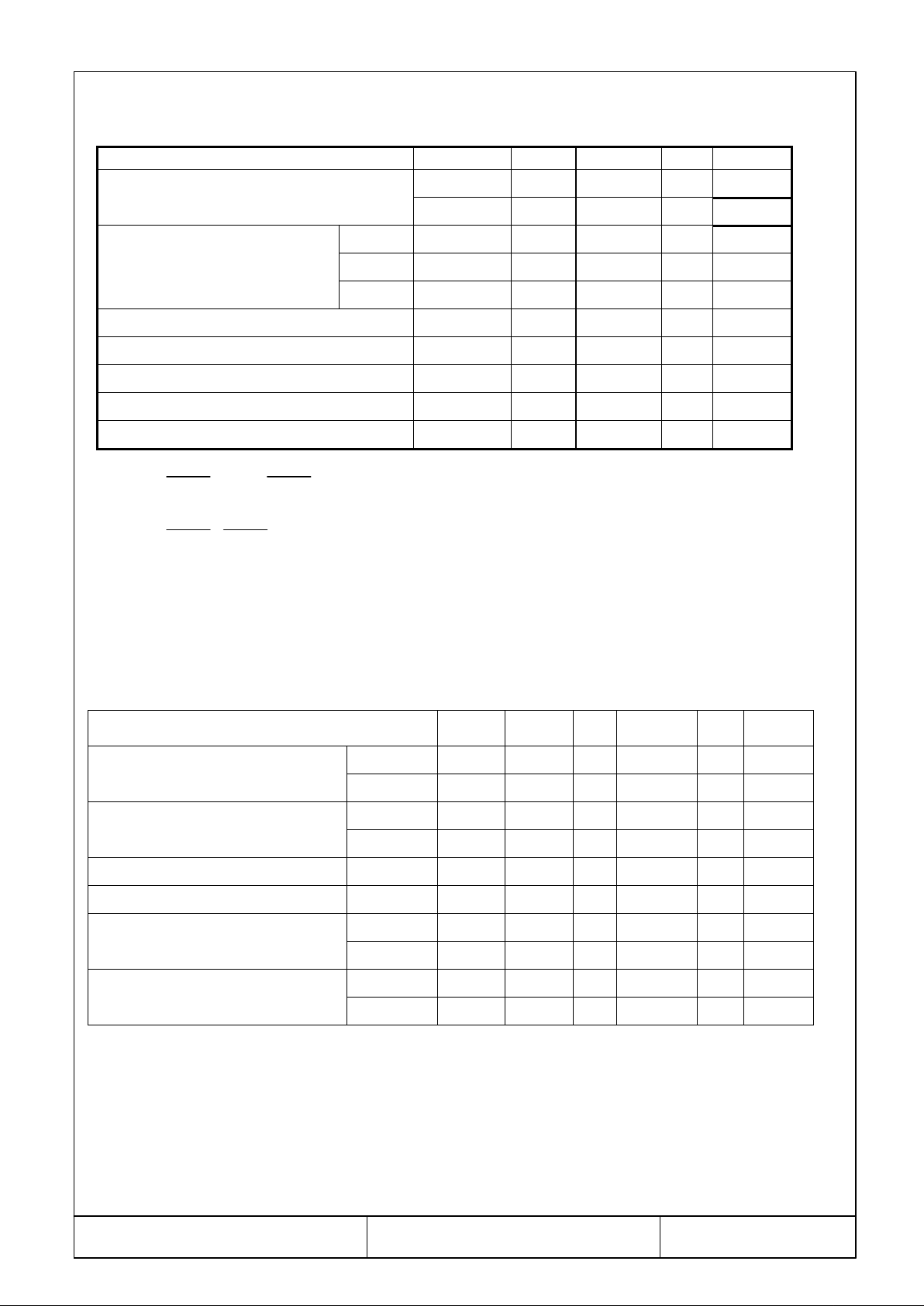
6. Absolute Maximum Ratings :
GND = 0 V,Ta = 25
Parameter Symbol MIN. MAX. Unit Remark
Supply Voltage For Source Driver
V
V
CC
DD
-0.5 7 V
-0.5 7 V
℃
Supply Voltage For Gate Driver
V
H Level V
L Level
VGL -20
GH-VGL
GH
-0.3 40 V
0 40 V
0 V
Analog Signal Input Level VR,VG,VB -0.3 7.0 V
Digital Input Signals -0.3 5.5 V Note 6-1
Digital Output Signals -0.3 5.5 V Note 6-2
Storage Temperature -30 +80
Operation Temperature -20 +70
℃
℃
Note 6-1 : HSY , CSY, VSY , CKC,
Note 6-2 : HSY , VSY , PSI, PSC
7. Electrical Characteristics
7-1) Recommended Operating Conditions:
A) Driving for TFT-LCD Panel
GND = 0V,Ta = 25
℃
Parameter Symbol MIN.
Analog V
CC
4.5 5.0 5.5 V
Typ MAX Unit Remark
Supply Voltage For Source Driver
Supply Voltage For Gate Driver
Logic V
H level V
L level V
DD
GH
GL
4.5 5.0 5.5 V
+15 +17 +19 V
-16 -15 -14 V
Supply Voltage For controller VDD 4.5 5.0 5.5 V
Analog Signal input Level
Amplitude 0.3 V
H level V
IH
0.7 V
DD
- V
0.3 V
CC-
DD
V
Digital input voltage
L level V
H level V
IL
OH
-0.3 - 0.3 V
0.7 V
DD
- V
DD
DD
V
V
Digital output voltage
L level V
OL
-0.3 - 0.3 V
DD
V
T-51446L050J-FW-P-AB
OPTREX CORPORATION
Page 6/21
Page 7

B) Driving for backlight
GH
Ta= 25
℃
Parameter Symbol Min. Typ. Max. Unit Remark
Lamp voltage V
Lamp current I
Lamp frequency P
Kick-off voltage(25℃)
Kick-off voltage(0℃)
L
L
L
Vs --- --- 345 Vrms Note 7-2
Vs
387 430 473 Vrms IL= 5 mA
4.5 5.0 5.5 mA
40 43 80 KHz Note 7-1
--- --- 520 Vrms Note 7-2
Note 7-1 : The wave form of lamp driving voltage should be as closed to a perfect SIN wave as possible.
Note 7-2 : The Kick-off times≧1sec
7-2) Power Consumption
Ta=
℃
25
Parameter Symbol Conditions TYP. MAX Unit Remark
Supply current for Gate Driver (Hi level) I
Supply current for Gate Driver (Low level) I
Supply current for Source Driver I
Supply current for controller I
GH
GL
CC
DD
V
V
V
V
GL
CC
DD
=
=
=
=
+17V
-15V
+5V
+5V
0.15 0.20 mA
-10.0 -15.0 mA
17.0 20.0 mA
43.0 48.0 mA
LCD Panel Power Consumption 0.45 0.57 W Note 7-3
Backlight Lamp Power Consumption 2.65 2.80 W Note 7-4
Note 7-3 : The power consumption for backlight is not included.
Note 7-4 : Backlight lamp power consumption is calculated by I
7-3) Input / Output signal timing chart
FRP
Black
V
R
V
G
V
B
Black
CSY
White
×
VL.
L
4.5V
5V
0V
f=15.4kHz
Vcom
T-51446L050J-FW-P-AB
OPTREX CORPORATION
6.0V
Page 7/21
Page 8

Parameter Symbol MIN. TYP. MAX. Unit Remarks
VPO(N)
Horizontal
Sync. Output
Pulse
Vertical Sync.
Output Pulse
Pulse Width T
Phase Difference T
Rising Time T
Falling Time T
Frequency
Pulse Width T
Difference
Phase
Difference
THP
NTSC FHO(N) - 15.73 - KHzFrequency
PAL FHO(P) - 15.63 - KHz
NTSC
PAL
NTSC T
PAL T
NTSC T
PAL T
HO
HP
HR
HF
VO
VPO(P)
VPE(N)
VPE(P)
4.4 4.7 5.0
0 2 -
- - 0.05
- - 0.05
fh/262.5
fh/312.5
- 4H - H
- 4H -Phase
- 4H -
- 4.5H -
- 3.5H -
μ
μ
μ
μ
H odd field
H even field
s
s
s
s
CSY
HSY
THR THF
THO
7-4) Display Time Range
A) When sync. Signal of NTSC system is applied.
a) Horizontally
11.35 ~ 61.36μs
b) Vertical
22 ~ 252 H
B) When sync. Signal of PAL system is applied.
a) Horizontally
11.54 ~ 61.9μs
b)
Vertical
29 ~ 301 H
SSSS
T-51446L050J-FW-P-AB
OPTREX CORPORATION
Page 8/21
Page 9

C) NTSC System
Timing chart of I/O and RGB signal
4H
Tvo
CMOS output
Tvo=254£gS Typ
Th Th=63.5£gS Typ
Black
Line
White
White
First
Black
ODD
FIELD
EVEN
FIELD
ODD FIELD
Tvpo=63.5£gS Typ
Tvpo
NTSC FIELD 1
524 525 1 2 3 4 5 6 7 8 9 10 23 24 25 26
Vin
CSY
T-51446L050J-FW-P-AB
258 259 260 261 262 1 2 3 4 5 6 7 20 21 22 23
HSY
VSY
OPTREX CORPORATION
FRP
RGB
Page 9/21
Page 10

line
Timing chart of I/O and RGB signal
White
Black
White
Black
Tvo=254£gS Typ
Tvo
4H
Tvpe
Tvpe=95£gS Typ
First
EVEN FIELD
NTSC FIELD 2
EVEN
FIELD
ODD
FIELD
262 263 264 265 266 267 268 269 270 271 272 285 286 287 288
Vin
CSY
HSY
VSY
259 260 261 262 263 1 2 3 4 5 6 20 21 2219
FRP
RGB
T-51446L050J-FW-P-AB
OPTREX CORPORATION
Page 10/21
Page 11

D) PAL System
V
CSY
HSY
VSY
FRP
RGB
Timing chart of I/O and RGB signal
ODD FIELD
2827
22
21
CMOS output
Tvo=318£gS Typ
Th=63.5£gS Typ
Tvo
Th
4H
26
28
22
27
Black
Black
Line
First
White
White
ODD
FIELD
EVEN
FIELD
Tvpo=64£gS Typ
Tvpo
FIELD 1
PAL
622 623 624 625 1 2 3 4 5 6 7 23 24 25 26
in
310 311 312 313 1 2 3 4 5 6 7 21 23 24 25
T-51446L050J-FW-P-AB
OPTREX CORPORATION
Page 11/21
Page 12

Timing chart of I/O and RGB signal
29
341
340
335
28
Black
White
Black
White
23
22 27
4H
Tvo
Tvo=318£gS Typ
White
White
line
First
Black
EVEN FIELD
Tvpe=32£gS Typ
Tvpe
PAL FIELD 2
EVEN
FIELD
ODD
FIELD
309 310 311 312 313 314 315 316 317 318 336 337 338 339
Vin
CSY
HSY
VSY
308 309 310 311 312 1 2 3 4 5 24 25 26
FRP
RGB
T-51446L050J-FW-P-AB
OPTREX CORPORATION
Page 12/21
Page 13

E) Display Timing FOR NTSC & PAL
VSY
Not Display Time
28.5/262.5=11%
234/262.5=89%
28.5H
Sampling Clock: 6.4MHz
s
m
2.14
10
Display Time
234 H
Line
First
22H
Tvo
Tvo=1H Typ
Tvo
s
m
63.5
50.01 ms
s
m
11.35
s
m
Tho=4.7
Display Time
50.01/63.5=79%
ODD FIELD
Tvpo=1H Typ
Tvpo
NTSC FIELD 1
ODD FIELD
524 525 1 2 3 4 5 6 7 8 9 22 23 24
EVEN FIELD
EVEN FIELD
NTSC FIELD 2
264 265 266 267 268 269 270 271 272 283 284 285 286
EVEN
3
26
262
Tvo=4H Typ
Tvpe
Tvpe=1.5H Typ
FIELD
ODD
FIELD
8.5H
(1) Horizontal Timing
(2) Vertical Timing
Vin
Vin
VSY
T-51446L050J-FW-P-AB
OPTREX CORPORATION
Page 13/21
Page 14

33
79.4/317.5=25%
28.5H
234 H
Display Time
339
338
7
234/317.5=75%
Line
First
Sampling Clock: 6.35MHz
334 335 336
s
m
64
21
s
m
2.1
ODD FIELD
s
m
Display Time
50.36
s
m
11.54
s
m
Tho=4.7
50.36/64=79%
20
EVEN FIELD
Tvo
Tvo=5H Typ
Tvpo=1H Typ
Tvpo
PAL FIELD 1
PAL FIELD 2
333
318
Tvo=5H Typ
Tvpe=0.5H Typ
28H
Tvo
Tvpe
(1) Horizontal Timing
(2) Vertical Timing
T-51446L050J-FW-P-AB
ODD
FIELD
EVEN
FIELD
622 623 624 625 1 2 3 4 5 6 7 22 23 24 25
Vin
VSY
OPTREX CORPORATION
EVEN
FIELD
ODD
FIELD
309 310 311 312 313 314 315 316 317
Vin
VSY
8.5H
Not Display Time
Page 14/21
Page 15

8. Power On Sequence
V
GH
0V(Gnd)
OFF
1) 10ms≦T1≦T2≦T3
2) 10ms≦T4≦T5≦T6
T1
T2
VCC,V
DD
V
GL
ON
T3 T4 T5 T6
Logic,VCom,
Video signal
OFF
T-51446L050J-FW-P-AB
OPTREX CORPORATION
Page 15/21
Page 16

9. Optical Characteristics
9-1) Specification:
Ta = 25
Parameter Symbol Condition MIN. TYP. MAX. Unit Remarks
Viewing Horizontal
Angle Vertical
Contrast Ratio CR
Response time Rise Tr
Fall Tf --- 30 50 ms
Transmission Ratio 8.0 8.5 --- %
Uniformity U 70 85 --- % Note 9-5
Brightness 350 400 ---
White x
Chromaticity y
Lamp Life Time
Note 9-1 : The definitions of viewing angles
+25
℃
θ
21,θ22
θ
11 CR≧10
θ
12
θ=0°
θ=0°
θ=0°
θ=0°
45 55 --- deg Note 9-1
10 15 --- deg Note 9-1
30 35 --- deg Note 9-1
80 150 --- Note 9-2
--- 15 30 ms Note 9-4
Note 9-3
㎡
cd/
0.250 0.300 0.350 Note 9-3
0.300 0.350 0.400
10,000 --- --- hr
℃
T-51446L050J-FW-P-AB
OPTREX CORPORATION
Page 16/21
Page 17

Luminance when Testing point is White
Tr
Tf
Note 9-2 : CR
=
Luminance when Testing point is Black
(Testing configuration see 9-2 )
Contrast Ratio is measured in optimum common electrode voltage.
Note 9-3 : Topcon BM-7(fast) luminance meter 2°field of view is used in the testing (after
20~30 minutes operation).
Lamp Current 5mA
Note 9-4 : The definition of response time :
W hite W hite
100%
90%
Brightness
10%
0%
Black
Note 9-5: The uniformity of LCD is defined as
The Minimum Brightness of the 9 testing Points
U =
The Maximum Brightness of the 9 testing
Points
Luminance meter : BM-5A or BM-7 fast(TOPCON)
Measurement distance : 500 mm +/- 50 mm
Ambient illumination : < 1Lux
Measuring direction : Perpendicular to the surface of module
The test pattern is white (Gray Level 63).
25% 50% 75%
T-51446L050J-FW-P-AB
25%
50%
75%
OPTREX CORPORATION
Page 17/21
Page 18

9-2) Testing configuration
BM-7(fast)
R,G,B signal
Pattern
generator
LCDDisplay
Ÿ
Caution: 1. Environmental illumination
2. Beforetest CR, Vcom voltage must
500mm
be adjusted carefully to get the best
CR.
input
LCD
Backlight
Testing Point Testing Point
Pattern A PatternB
。 リ
1 lux
R, G, B Waveformof Pattern A at Testing Point
Ÿ
16ms 16ms
Vw=1.3V+/-0.2V
R, G, B Waveformof Pattern B at Testing Point
Ÿ
16ms 16ms
Vb=5.0V+/-0.2V
RGB
waveform
RGB
waveform
Vcom
Vcom
T-51446L050J-FW-P-AB
OPTREX CORPORATION
Page 18/21
Page 19

10. Handling Cautions
10-1) Mounting of module
a) Please power off the module when you connect the input/output connector.
b) Please connect the ground pattern of the inverter circuit surely. If the connection
is not perfect, some following problems may happen possibly.
1.The noise from the backlight unit will increase.
2.The output from inverter circuit will be unstable.
3.In some cases a part of module will heat.
c) Polarizer which is made of soft material and susceptible to flaw must be
handled carefully.
d) Protective film (Laminator) is applied on surface to protect it against scratches
and dirts. It is recommended to peel off the laminator before use and taking
care of static electricity.
10-2) Precautions in mounting
a) When metal part of the TFT-LCD module (shielding lid and rear case) is soiled,
wipe it with soft dry cloth.
b) Wipe off water drops or finger grease immediately. Long contact with water may
cause discoloration or spots.
c) TFT-LCD module uses glass which breaks or cracks easily if dropped or bumped on
hard surface. Please handle with care.
d) Since CMOS LSI is used in the module. So take care of static electricity and
earth yourself when handling.
10-3) Adjusting module
a) Adjusting volumes on the rear face of the module have been set optimally before
shipment.
b) Therefore, do not change any adjusted values. If adjusted values are changed, the
specifications described may not be satisfied.
10-4) Others
a) Do not expose the module to direct sunlight or intensive ultraviolet rays for many
hours.
b) Store the module at a room temperature place.
c) The voltage of beginning electric discharge may over the normal voltage because of
leakage current from approach conductor by to draw lump read lead line around.
d) If LCD panel breaks, it is possibly that the liquid crystal escapes from the panel.
Avoid putting it into eyes or mouth. When liquid crystal sticks on hands, clothes or
feet. Wash it out immediately with soap.
e) Observe all other precautionary requirements in handling general electronic
components.
f) Please adjust the voltage of common electrode as material of attachment by 1 module.
T-51446L050J-FW-P-AB
OPTREX CORPORATION
Page 19/21
Page 20

11
. Reliability Test
No Test Item Test Condition
1 High Temperature Storage Test
2 Low Temperature Storage Test
3 High Temperature Operation Test
4 Low Temperature Operation Test
5
6
7
8
9
High Temperature & High
Humidity Operation Test
Thermal Cycling Test
(non-operating)
Vibration Test
(non-operating)
Shock Test
(non-operating)
Electrostatic Discharge Test
(non-operating)
-25℃ →+25℃→ +70℃, 200 Cycles
30 min 5min 30 min
Test Period: 6 Cycles for each direction of X, Y, Z
10 times/point, 5 points/panel face
Ta = +80 ℃, 240 hrs
Ta = -30℃, 240 hrs
Ta = +70 ℃, 240 hrs
Ta = -20 ℃, 240 hrs
Ta = +60℃, 95%RH, 240 hrs
Frequency:10 ~ 55 H
Amplitude:1.5 mm
Sweep time: 11 mins
100G, 6ms
Direction: ±X, ±Y, ±Z
Cycle: 3 times
150pF, 330Ω
Air: ±15KV; Contact: ±8KV
Z
Ta: ambient temperature
[Criteria]
Under the display quality test conditions with normal operation state, there should be no change
which may affect practical display function.
12. Indication of Lot Number Label
a) Indicated contents of the label
Lot number
OOO-OOOOOO
T-51446L050J-FW-P-AB
Module number
Contents of lot number : 1st—Process area : class 1000ÞH
class 100KÞM
2nd~3rd—Module screen size(in inch) : 1.8”Þ18, 2.5”Þ25……
5th—Production year : 1999Þ9, 2000ÞA, 2001Þ1……..
6th—Production month : 1, 2, 3,….9, A, B, C
7th~10th—Serial numbers : 0001~9999
T-51446L050J-FW-P-AB
OPTREX CORPORATION
Page 20/21
Page 21

13. Block Diagram
HSY
VSY
CSY
CKC
U/D
R/L
N/P
FRP
PSI
PSC
+5 V
+17 V
‑15V
VR
VG
VB
Controller
PLL VL
V Driver
(Gate)
VCO
LCD Panel
H Driver
(Source)
R1G1B1
Back‑lightInverter
T-51446L050J-FW-P-AB
OPTREX CORPORATION
Page 21/21
 Loading...