

Page 1
Rev.
Date
Page
Comment
OP T R E X
LCD Module Technical Specification
T-51410D104-FW-P-AF
First Edition
Dec 5, 2001
Final Revision
******
Checked by (Quality Assurance Div.)
***The part number and specification are still tentative.
Table of Contents
1. Applications................................................................................................................................................. 2
2. Features........................................................................................................................................................... 2
3. Mechanical Specifications................................................................................................................ 2
4. Mechanical Drawing TFT LCD Module ............................................................................ 3
5. Input / Output Terminals................................................................................................................. 4
6. Absolute Maximum Ratings.............................................................................................................6
7. Electrical Characteristics.....................................................................................................................6
8. Power Sequence.................................................................................................................................... 12
9. Optical Characteristics ..................................................................................................................... 13
10. Handling Cautions............................................................................................................................... 16
11. Reliability TEST.....................................................................................................................................17
12. Block Diagram.........................................................................................................................................18
Checked by (Design Engineering Div.)
Prepared by (Production Div.)
Revision History
T-51410D104-FW-P-AF
OPTREX CORPORATION
Page 1/18
Page 2
1.Application
This data sheet applies to a color TFT LCD module, T-51410D104-FW-P-AF.
T-51410D104-FW-P-AF module applies to notebook PC, sub-note-book PC and other OA
product, which require high quality flat panel display.
This module is not designed for
aerospace, avionics, medical, F/A, transportation, car or any other products, which require
extreme level of reliability.
Optrex assumes no responsibility for any damage resulting from the use of the device which
dose not comply with the instructions and the precautions inthese specification sheet.
2. Features
. Amorphous silicon TFT LCD panel with back-light unit
. Pixel in stripe configuration
. Slim and compact, designed for O/A application
. Display Colors:262,144 colors
. Optimum Viewing Direction:12 o’clock
. 3.3V LVDS interface standard: DS90CF364 as receiver
. +3.3V DC supply voltage for TFT LCD panel driving
. Backlight driving DC/AC inverter not included in this module
. Wide Viewing Angle
3.Mechanical Specifications
Parameter Specifications Unit
Screen Size 26.4(diagonal) cm
10.4 (diagonal) inch
Display Format
Display Colors 262,144
Active Area
Pixel Pitch
Pixel Configuration Stripe
Outline Dimension
Weight 310(typ.),320(max.) g
Back-light Single CCFL, side-light type
Surface treatment Anti-glare and hard-coating
Display mode Normally white
800×(R, G, B)×600
211.2(H)×158.4 (V)
0.264 (H)×0.264 (V)
238.6 (w)×171.0(H)×6.0(typ.) (D)
dot
mm
mm
mm
T-51410D104-FW-P-AF
OPTREX CORPORATION
Page 2/18
Page 3
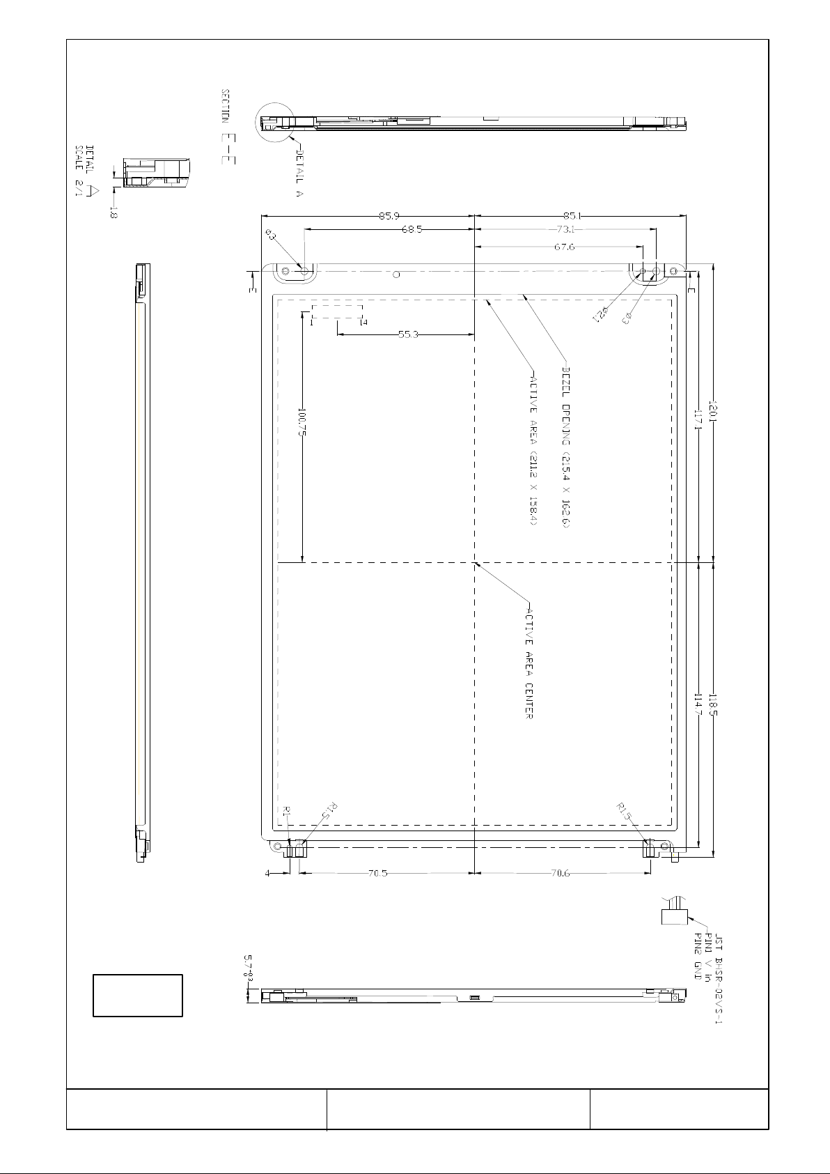
4.Mechanical Drawing of TFT-LCD Module
Unit: mm
T-51410D104-FW-P-AF
OPTREX CORPORATION
Page 3/18
Page 4
5.Input Terminals
5-1) TFT-LCD Panel Driving
Connector type: Molex55177-1491
Pin No. Symbol Function Remark
1 VDD Power supply : +3.3V
2 VDD Power supply : +3.3V
3 GND
4 GND
5 IN0- Pixel data Transmission pair 0 (negative -)
6 IN0+ Pixel data Transmission pair 0 (positive +)
7 IN1- Pixel data Transmission pair 1 (negative -)
8 IN1+ Pixel data Transmission pair 1 (positive +)
9 IN2- Pixel data Transmission pair 2 (negative -)
10 IN2+ Pixel data Transmission pair 2 (positive +)
11 CLK- Sampling Clock (negative -)
12 CLK+ Sampling Clock (positive +)
13 GND
14 GND
Recommended Transmitter (DS90C*363 of National Semiconductor) toT-51410D104-FW-
P-AF interface Assignment:
Input
terminal
of DS
Symbol No. Symbol Function
TIN0 44 R0 Red pixel data (LSB)
TIN1 45 R1 Red pixel data
TIN2 47 R2 Red pixel data Tout0- No.5 : IN0TIN3 48 R3 Red pixel data
TIN4 1 R4 Red pixel data Tout0+ No.6 : IN0+
TIN5 3 R5 Red pixel data(MSB)
TIN6 4 G0 Green pixel data (LSB)
TIN7 6 G1 Green pixel data
TIN8 7 G2 Green pixel data
TIN9 9 G3 Green pixel data Tout1- No.7 : IN1TIN10 10 G4 Green pixel data
TIN11 12 G5 Green pixel data(MSB) Tout1+ No.8 : IN1+
TIN12 13 B0 Blue pixel data(LSB)
TIN13 15 B1 Blue pixel data
TIN14 16 B2 Blue pixel data
TIN15 18 B3 Blue pixel data
TIN16 19 B4 Blue pixel data Tout2- No.9 : IN2TIN17 20 B5 Blue pixel data(MSB)
TIN18 22 NC No connection Tout2+ N0.10 : IN2+
TIN19 23 NC No connection
TIN20 25 ENAB Compound Synchronization
CLK in 26 NCLK Data sampling clock TCLK out-
90C*363
Graphic controller output signal Output signal
symbol
signal
TCLK out+
To T-51410D104-
FW-P-AF interface
terminal(Symbol)
No.11 : CLK INNo.12 : CLK IN+
T-51410D104-FW-P-AF
OPTREX CORPORATION
Page 4/18
Page 5
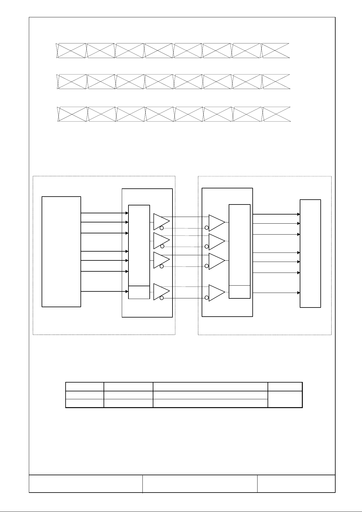
Data stream of IN0-/+, IN1-/+ and IN2-/+ for T-51410D104-FW-P-AF
GraphicController Circuit
TTLparallel to LVDS
LVDS to TTL parallel
LCD Internal Circuit
T-51410D104-FW-P-AF Module
IN0
IN1
RxOUT6 RxOUT5 RxOUT4 RxOUT3 RxOUT2
G0
RxOUT13 RxOUT12 RxOUT11 RxOUT10 RxOUT9
B1
IN2
RxOUT13 RxOUT12 RxOUT11 RxOUT10 RxOUT9
ENAB
R5
B0
NC
LVDS Interface Block Diagram
R0~R5
G0~G5
B0~B5
TIN0~TIN5
TIN6~TIN11
TIN12~TIN17
R4 R3 R2
G5 G4 G3
NC B5 B4
IN0IN0+
IN1-
RxOUT1
R1 R0
RxOUT8
G2 G1
RxOUT8
B3 B2
RxOUT0
RxOUT7
RxOUT7
RxOUT0~RxOUT5
RxOUT6~RxOUT11
RxOUT12~RxOUT17
TIN18
NC
TIN19
NC
ENAB
CLK IN
TIN20
TCLK IN
Customer systemside
PLL
DS90C*363
IN1+
IN2-
IN2+
CLKCLK+
RxOUT18
RxOUT19
RxOUT20
CLKOUT
PLL
DS90CF364
PD104SL6 moduleside
5-2) Backlight driving
Connector type :“BHR-02VS-1” of Japan Solderless Terminal MFG Co. LTD
PIN NO. Symbol Description Remark
1 VL1 Input Voltage(High)
2 VL2 Input Voltage(Low)
T-51410D104-FW-P-AF
OPTREX CORPORATION
Page 5/18
Page 6
6.Absolute Maximum Ratings:
1234567
8
Parameters Symbol MIN. MAX. Unit Remark
Supply Voltage VDD -0.3 +4.0 V
Input Signals Voltage V
Backlight Driving Voltage V
Backlight Driving Frequency F
Storage Temperature T
Operating Temperature T
IN
L
L
ST
OP
-0.3 VDD+0.3 V Note 6-1
- 2000 V
0 100 KHz
-20 +70 C
0 +60 C
Note 6-1: LVDS signal
7.Electrical Characteristics
GND=0V, Ta=25C
7-1) Recommended Operating Conditions: GND = 0V,Ta = 25
Item Symbol Min. Typ. Max. Unit Remark
Supply Voltage VDD 3.0 3.3 3.6 V
Current Dissipation I
LVDS Differential input high threshold V
LVDS Differential input low threshold V
Lamp Current I
DD
TH
TL
FL
- 350 450 mA Note 7-1
- - 100 mV Note 7-2
-100 - -
3.0 7.0 - mA
Note 7-3
Note 7-5
Lamp Voltage V
Lamp Initial Voltage V
Lamp Driving Frequency F
L
SFL
L
500 550 600 Vrms Note 7-3
- 1200 - Vrms
1000
at Ta=25°C
at Ta=0°C
- 45 - KHz
Total power consumption (at IFL=7mA) - 5.01 - W Note 7-4
Note 7-1 : To test the current dissipation of VDD, using the“color bars” testing pattern
shown as below
White
1.
Yellow
2.
Cyan
3.
Green
4.
Magenta
5.
Red
6.
Blue
7.
Black
8.
℃
Idd current dissipation testing pattern
T-51410D104-FW-P-AF
OPTREX CORPORATION
Page 6/18
Page 7

Note 7-2 : Please refers to DS90CF364 specification by National Semiconductor
Yokogawa 2016-01
X,1
X,2
X,3
X,4
X,598
X,599
X,600
X,Y
0
Corporation. This LCD module conforms to LVDS standard.
Note 7-3 : The back-light driving waveform should be as closed to sine-wave as possible.
In order to satisfy the quality of B/L , no matter use what kind of inverter , the output
lamp current must between Min. and Max. to avoid the abnormal display image
caused by B/L.
Note 7-4 : Not including the efficiency of backlight DC/AC inverter
Note 7-5 : Lamp current is measured with current meter for high frequency as shown below
TFT-LCD
Module
* Pin 2 is V
low
** Current meter :
Lamp current dissipation testing configuration
7-2) Input / Output signal timing chart
(A) Vertical Timing
1
t
2
t
CLK
1
Inverter
2
~
A
ENAB
R5~R0
G5~G
B5~B0
3
3
t
t
T-51410D104-FW-P-AF
OPTREX CORPORATION
Page 7/18
Page 8

(B) Horizontal Timing
t
CLK
ENAB
R5~R0
3
t
4
t
c
797,Y 799,Y
G5~G0
B5~B0
CLK
ENAB
R5‑R0
G5‑G0
B5‑B0
2,Y 3,Y 4,Y 5,Y
1,Y
t 6
7,Y
6,Y
t 5
t 8 t 9
X,Y
t 7
VALID
DATA
798,Y 800,Y
VIH(Min):0.8V
VIL(Max):0.2V
Input Signal
CenterLevel:
0.5V
VIH(Min):0.8V
VIL(Max):0.2V
cc
cc
cc
cc
cc
a
CLK
Duty ( a ,b ) : 50 。モ 10%
T-51410D104-FW-P-AF
b
0.5V
cc
OPTREX CORPORATION
Page 8/18
Page 9

D) Timing Specifications
Item Symbol Min. Typ. Max. Unit Remark
Frame Cycling t1 604 X t3 628X t3 660 X t3 -
- 16.58 17.86 ms
Vertical Display Period t2 600 X t3 600 X t3 600 X t3 Horizontal Scanning Time t3 844 X t5 1056 X t5 1064 X t5 -
26.3 26.4 Horizontal Display Period t4 - 800 X t5 - Clock Cycle t5 24.0 25.0 - ns
Clock High Level Time t6 9.0 - - ns
Clock Low Level Time t7 9.0 - - ns
Hold time t8 4.0 - - ns
Set-up time t9 5.0 - - ns
μ
s
T-51410D104-FW-P-AF
OPTREX CORPORATION
Page 9/18
Page 10

7-3) Display Color and Gray Scale Reference
Input Color Data
Color Red Green Blue
R5 R4 R3 R2 R1 R0 G5 G4 G3 G2 G1 G0 B5 B4 B3 B2 B1 B0
Black 0 0 0 0 0 0 0 0 0 0 0 0 0 0 0 0 0 0
Red (63) 1 1 1 1 1 1 0 0 0 0 0 0 0 0 0 0 0 0
Green
(63)
Basic Blue (63) 0 0 0 0 0 0 0 0 0 0 0 0 1 1 1 1 1 1
Colors Cyan 0 0 0 0 0 0 1 1 1 1 1 1 1 1 1 1 1 1
Magenta 1 1 1 1 1 1 0 0 0 0 0 0 1 1 1 1 1 1
Yellow 1 1 1 1 1 1 1 1 1 1 1 1 0 0 0 0 0 0
White 1 1 1 1 1 1 1 1 1 1 1 1 1 1 1 1 1 1
Red (00) 0 0 0 0 0 0 0 0 0 0 0 0 0 0 0 0 0 0
Red (01) 0 0 0 0 0 1 0 0 0 0 0 0 0 0 0 0 0 0
Red (02) 0 0 0 0 1 0 0 0 0 0 0 0 0 0 0 0 0 0
Darker
Red
Green
Blue
↓ ↓ ↓ ↓ ↓ ↓ ↓ ↓ ↓ ↓ ↓ ↓ ↓ ↓ ↓ ↓ ↓ ↓ ↓
Brighter
Red (61) 1 1 1 1 0 1 0 0 0 0 0 0 0 0 0 0 0 0
Red (62) 1 1 1 1 1 0 0 0 0 0 0 0 0 0 0 0 0 0
Red (63) 1 1 1 1 1 1 0 0 0 0 0 0 0 0 0 0 0 0
Green
(00)
Green
(01)
Green
(02)
Darker
↓ ↓ ↓ ↓ ↓ ↓ ↓ ↓ ↓ ↓ ↓ ↓ ↓ ↓ ↓ ↓ ↓ ↓ ↓
Brighter
Green
(61)
Green
(62)
Green
(63)
Blue (00) 0 0 0 0 0 0 0 0 0 0 0 0 0 0 0 0 0 0
Blue (01) 0 0 0 0 0 0 0 0 0 0 0 0 0 0 0 0 0 1
Blue (02) 0 0 0 0 0 0 0 0 0 0 0 0 0 0 0 0 1 0
Darker
↓ ↓ ↓ ↓ ↓ ↓ ↓ ↓ ↓ ↓ ↓ ↓ ↓ ↓ ↓ ↓ ↓ ↓ ↓
Brighter
Blue (61) 0 0 0 0 0 0 0 0 0 0 0 0 1 1 1 1 0 1
Blue (62) 0 0 0 0 0 0 0 0 0 0 0 0 1 1 1 1 1 0
Blue (63) 0 0 0 0 0 0 0 0 0 0 0 0 1 1 1 1 1 1
0 0 0 0 0 0 1 1 1 1 1 1 0 0 0 0 0 0
0 0 0 0 0 0 0 0 0 0 0 0 0 0 0 0 0 0
0 0 0 0 0 0 0 0 0 0 0 1 0 0 0 0 0 0
0 0 0 0 0 0 0 0 0 0 1 0 0 0 0 0 0 0
0 0 0 0 0 0 1 1 1 1 0 1 0 0 0 0 0 0
0 0 0 0 0 0 1 1 1 1 1 0 0 0 0 0 0 0
0 0 0 0 0 0 1 1 1 1 1 1 0 0 0 0 0 0
T-51410D104-FW-P-AF
OPTREX CORPORATION
Page 10/18
Page 11

7-4) Pixel Arrangement
RGBRGBRGBRGBRGBRGBRGBRGBRGBRGBRGBRGBRGBRGB3
rd Line
2
nd Line
1
st Line
600
th Line
599
th Line
598
th Line
RGBRGBRGBRGB1
st Pixel
800
th Pixel
1 Pixel=
RGB
The LCD module pixel arrangement is the stripe.
T-51410D104-FW-P-AF
OPTREX CORPORATION
Page 11/18
Page 12

8.)Power On Sequence
3.0 V
V
CC
0 s< t <35 ms
0 s< t <35 ms
Signal
2t
1
0<t
Backlight
1. The supply voltage for input signals should be same as V
3.0 V
1
CC.
2. When the power is off , please keep whole signals (Hsync, Vsync, CLK, Data) low level
or high impedance
9.) Optical Characteristics
T-51410D104-FW-P-AF
OPTREX CORPORATION
Page 12/18
Page 13

9-1) Specification:
500 mm +/- 50 mm
Ta = 25
Parameter Symbol Condition MIN. TYP. MAX. Unit Remarks
Horizontal
Viewing Angle
Contrast Ratio CR
Response time
Luminance L
Luminance Uniformity U 55 80 - % Note 9-5
Lamp Life Time
Cross Talk Ratio CTK - - 3.5 % Note 9-6
Vertical
Rise Tr - 15 30 ms
Fall Tf
θ ±
θ
(to 12
o’clock)
θ
(to 6
o’clock)
x 0.266 0.316 0.366 y 0.293 0.343 0.393 -White Chromaticity
Tc 6400 6600 6800 K
CR³10
Optimum
direction
θ=0°
φ=0°
θ
=0°/
°
=0
φ
50 55 - deg Note 9-1
35 40 - deg
100 180 - - Note 9-2
200 230 -
1000
±
55
- 25 50 ms
0
60
- - hr IFL=7mA
- deg
cd/
Note 9-4
IFL=7mA, Note 9-
㎡
3
℃
All the optical measurement shall be executed 30 minutes after backlight being turn-on. The
optical characteristics shall be measured in dark room (ambient illumination on panel surface
less than 1 Lux). The measuring configuration shows as following figure.
Photometer (TOPCON
BM-5A or BM-7 fast)
Field = 2°
TFT-LCD module
DC/AC Inverter
Optical characteristics measuring configuration
T-51410D104-FW-P-AF
OPTREX CORPORATION
Page 13/18
Page 14

Note 9-1`:The definitions of viewing angles are as follows.
12 o’clock
3 o’clock
9 o’clock
6 o’clock
B
Tr
Tf
q
f
Lamp connector
Note 9-2 : The definition of contrast ratio
CR
=
Luminance atgray level 0
Note 9-3:Topcon BM-5A luminance meter 2°field of view is used in the testing (after 30
minutes’ operation). The typical luminance value is measured at lamp current 7.0mA.
Note 9-4: Definition of Response Time Trand Tf:
Luminance atgray level 63
White White
100%
90%
rightness
10%
0%
Black
Note 9-5: The uniformity of LCD is defined as
The Minimum Brightness of the 9 testing Points
U =
The Maximum Brightness of the 9 testing
Points
Luminance meter : BM-5A or BM-7 fast(TOPCON)
Measurement distance : 500 mm +/- 50 mm
Ambient illumination : < 1 Lux
Measuring direction : Perpendicular to the surface of module
The test pattern is white (Gray Level 63).
T-51410D104-FW-P-AF
OPTREX CORPORATION
Page 14/18
Page 15

25% 50% 75%
25%
50%
75%
Note 9-6: Cross Talk (CTK) =
YA: Brightness of Pattern A
YB: Brightness of Pattern B
Luminance meter : BM 5A (TOPCON)
Measurement distance : 500 mm +/- 50 mm
Ambient illumination : < 1 Lux
Measuring direction : Perpendicular to the surface of module
Pattern A
(GrayLevel 31)
½YA-YB½
YA
YA
×
1/3
1/3
1/3
100%
Pattern B
(GrayLevel 31, central
black box exclusive)
YB
: Measuring Point (A and B are at the same point.)
T-51410D104-FW-P-AF
1/3 1/3 1/3
OPTREX CORPORATION
Black
(GrayLevel 0)
Page 15/18
Page 16

10. Handling Cautions
10-1) Mounting of module
a) Please power off the module when you connect the input/output connector.
b) Please connect the ground pattern of the inverter circuit surely. If the connection
is not perfect, some following problems may happen possibly.
1.The noise from the backlight unit will increase.
2.The output from inverter circuit will be unstable.
3.In some cases a part of module will heat.
c) Polarizer which is made of soft material and susceptible to flaw must be
handled carefully.
d) Protective film (Laminator) is applied on surface to protect it against scratches
and dirts. It is recommended to peel off the laminator before use and taking
care of static electricity.
10-2) Precautions in mounting
a) When metal part of the TFT-LCD module (shielding lid and rear case) is soiled,
wipe it with soft dry cloth.
b) Wipe off water drops or finger grease immediately. Long contact with water may
cause discoloration or spots.
c) TFT-LCD module uses glass which breaks or cracks easily if dropped or
bumped on hard surface. Please handle with care.
d) Since CMOS LSI is used in the module. So take care of static electricity and
earth yourself when handling.
10-3) Adjusting module
a) Adjusting volumes on the rear face of the module have been set optimally
before shipment.
b) Therefore, do not change any adjusted values. If adjusted values are changed,
the specifications described may not be satisfied.
10-4) Others
a) Do not expose the module to direct sunlight or intensive ultraviolet rays for many
hours.
b) Store the module at a room temperature place.
c) The voltage of beginning electric discharge may over the normal voltage
because of leakage current from approach conductor by to draw lump read lead
line around.
d) If LCD panel breaks, it is possibly that the liquid crystal escapes from the panel.
Avoid putting it into eyes or mouth. When liquid crystal sticks on hands, clothes
or feet. Wash it out immediately with soap.
e) Observe all other precautionary requirements in handling general electronic
components.
f) Please adjust the voltage of common electrode as material of attachment by 1
module.
T-51410D104-FW-P-AF
OPTREX CORPORATION
Page 16/18
Page 17

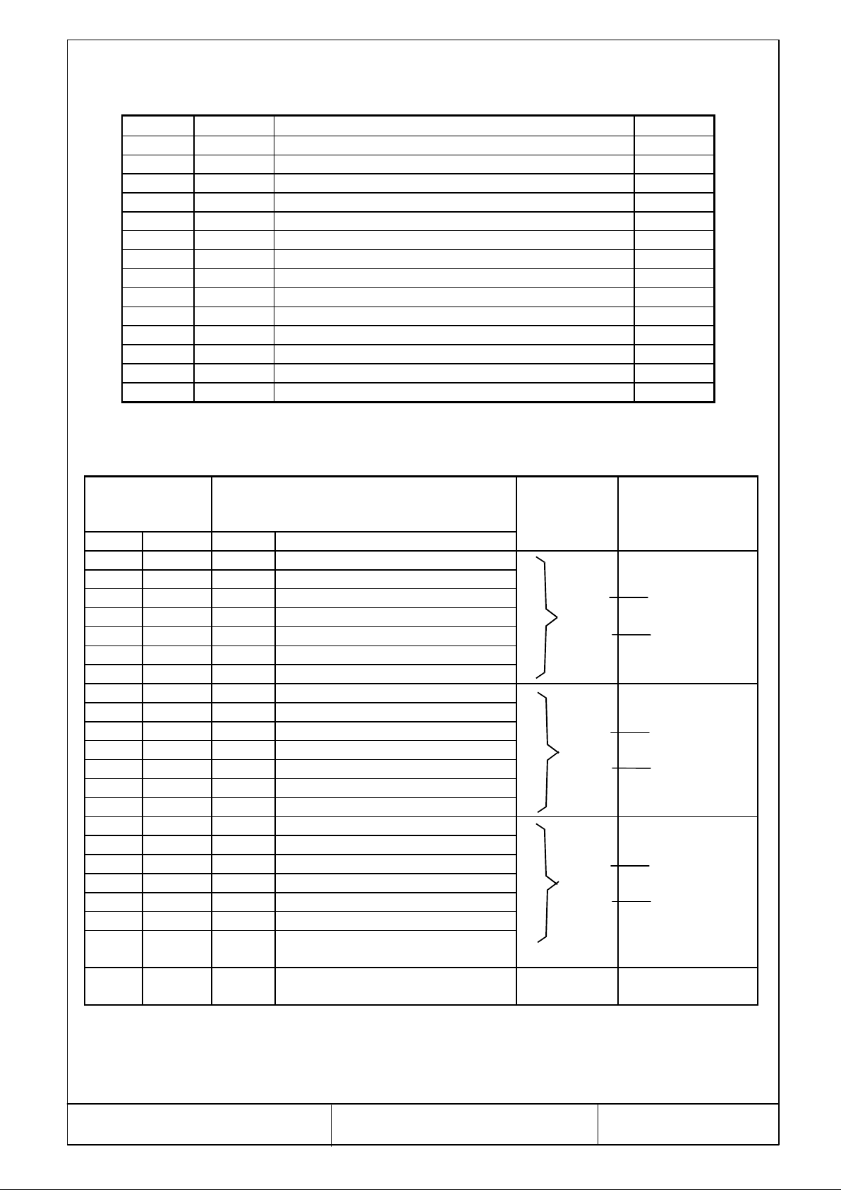
11. Reliability Test
No Test Item Test Condition Remark
1 High Temperature Storage Test
2 Low Temperature Storage Test
3 Low Temperature Operation Test
High Temperature & High Humidity
4
Operation Test
Thermal Cycling Test
5
(non-operating)
Vibration Test
6
(non-operating)
Shock Test
7
(non-operating)
Ta: ambient temperature
Ta = +70℃, 240 hrs
Ta = -20℃, 240 hrs
Ta = 0℃, 240 hrs
Ta = +60℃, 80%RH, 240 hrs
(No Condensation)
0
℃
ßà+25℃ßà+60
1Hr 0.5Hr 1Hr
Frequency:10 ~ 57 H
58~500Hz, 1G
Sweep time: 11 min
Test Period: 3 hrs (1 hr for each direction of
X, Y, Z)
80G, 6ms, X,Y, Z
1 times for each direction
℃
, 50 Cycles
Amplitude:0.15 mm
Z ,
[Judgement Criteria]
Under the display quality test conditions with normal operation state , there should be no
change which may affect practical display function.
T-51410D104-FW-P-AF
OPTREX CORPORATION
Page 17/18
Page 18

12.)Block Diagram
1
23599
598
600
421
2400
Con
o
C
cu
G
D
r
LVD
D
C
R5G5B5
…
…
…
ENAB
CLK
Back-light(Lamp1)
VL1
VL2
ENAB
CLK
IN0-/+
IN1-/+
IN2-/+
VDD
S Interface(
S90
364)
Power
Module
R0
R1
G0
G11
B0
B1
tr
l
ir
ate
TFT-LCD
rive
Display Area
it
3
Source Driver
T-51410D104-FW-P-AF
OPTREX CORPORATION
Page 18/18
 Loading...